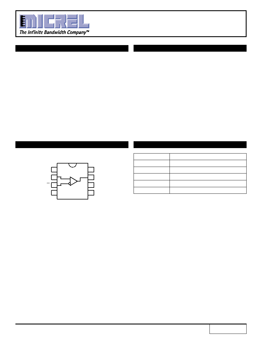
Pin
Function
Q
TTL Output
D, /D
Differential PECL Inputs
V
CC
+5.0V Supply
V
BB
Reference Output
GND
Ground
DESCRIPTION
s
2.5ns typical propagation delay
s
Low power
s
Differential PECL inputs
s
24mA TTL outputs
s
Flow-through pinouts
s
Available in 8-pin SOIC package
The SY10/100ELT21 are single differential PECL-to-
TTL translators. Because PECL (Positive ECL) levels are
used, only +5V and ground are required. The small outline
8-lead SOIC package and low skew single gate design
make the ELT21 ideal for applications that require the
translation of a clock or data signal where minimal space,
low power, and low cost are critical.
The V
BB
output allow differential single-ended, or AC-
coupled interface to the device. If used, the V
BB
output
should be bypassed to V
CC
with a 0.01
µ
F capacitor.
The ELT21 is available in both ECL standards: the
10ELT is compatible with positive ECL 10H logic levels,
while the 100ELT is compatible with positive ECL 100K
logic levels.
FEATURES
DIFFERENTIAL
PECL-to-TTL
TRANSLATOR
PIN NAMES
PIN CONFIGURATION/BLOCK DIAGRAM
SOIC
TOP VIEW
ClockWorksTM
SY10ELT21
SY100ELT21
FINAL
1
NC
D
D
V
BB
8
V
CC
Q
NC
GND
7
6
5
2
3
4
PECL
TTL
1
Rev.: B
Amendment: /0
Issue Date:
April 2000
2
ClockWorksTM
SY10ELT21
SY100ELT21
Micrel
Symbol
Parameter
Value
Unit
V
CC
Power Supply Voltage
≠0.5 to +7.0
V
V
I
PECL Input Voltage
0V to V
CC
+0.5
V
V
O
Voltage Applied to
≠0.5 to +5.5
V
Output at HIGH State
I
O
Current Applied to
Twice the
mA
Output at LOW State
Rated I
OL
T
store
Storage Temperature
≠65 to +150
∞
C
T
A
Operating Temperature
≠40 to +85
∞
C
NOTE:
1. Permanent device damage may occur if ABSOLUTE MAXIMUM RATINGS
are exceeded. This is a stress rating only and functional operation is not
implied at conditions other than those detailed in the operational sections
of this data sheet. Exposure to ABSOLUTE MAXIMUM RATlNG conditions
for extended periods may affect device reliability.
ABSOLUTE MAXIMUM RATINGS
(1)
TRUTH TABLE
D
/D
Q
L
H
L
H
L
H
Open
Open
L
T
A
= ≠40
∞
C
T
A
= 0
∞
C
T
A
= +25
∞
C
T
A
= +85
∞
C
Symbol
Parameter
Min.
Max.
Min.
Max.
Min.
Typ.
Max.
Min.
Max.
Unit
Condition
I
OS
Output Short Circuit Current
≠80
≠200
≠80
≠200
≠80
--
≠200
≠80
≠200
mA
V
OUT
= 0V
I
CC
Power Supply Current
--
20
--
20
--
14
20
--
20
mA
--
V
OH
Output HIGH Voltage
2.5
--
2.5
--
2.5
--
--
2.5
--
V
I
OH
= ≠3.0mA
2.0
--
2.0
--
2.0
--
--
2.0
--
V
I
OH
= ≠15mA
V
OL
Output LOW Voltage
--
0.5
--
0.5
--
--
0.5
--
0.5
V
I
OL
= 24mA
TTL DC ELECTRICAL CHARACTERISTICS
V
CC
= 4.75V to 5.25V
T
A
= ≠40
∞
C
T
A
= 0
∞
C
T
A
= +25
∞
C
T
A
= +85
∞
C
Symbol
Parameter
Min.
Max.
Min.
Max.
Min.
Typ.
Max.
Min.
Max.
Unit
Condition
I
IH
Input HIGH Current
--
150
--
150
--
--
150
--
150
µ
A
I
IL
Input LOW Current
0.5
--
0.5
--
0.5
--
--
0.5
--
µ
A
V
IH
Input HIGH Voltage
(2)
10ELT
3770
4110
3830
4160
3870
--
4190
3940
4280
mV
100ELT
3835
4120
3835
4120
3835
4120
3835
4120
V
IL
Input LOW Voltage
(2)
10ELT
3050
3500
3050
3520
3050
--
3520
3050
3555
mV
100ELT
3190
3525
3190
3525
3190
--
3525
3190
3525
V
BB
Reference Output
(2)
10ELT
3570
3700
3620
3730
3650
--
3750
3690
3810
mV
100ELT
3620
3740
3620
3740
3620
--
3740
3620
3740
PECL DC ELECTRICAL CHARACTERISTICS
V
CC
= 4.75V to 5.25V
NOTES:
1. These values are for V
CC
= 5.0V. Level Specifications will vary 1:1 V
CC
.
3
ClockWorksTM
SY10ELT21
SY100ELT21
Micrel
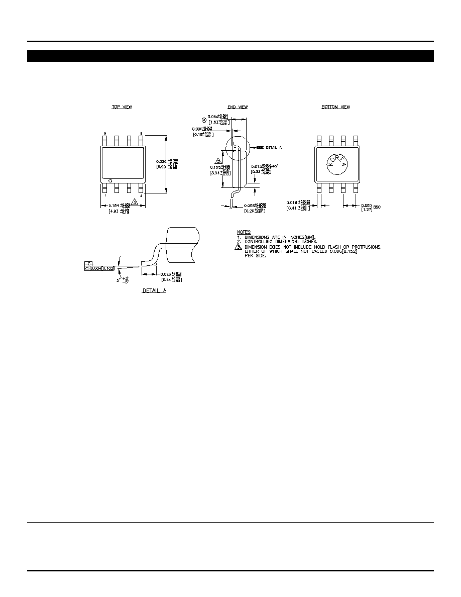
PRODUCT ORDERING CODE
Ordering
Package
Operating
V
CC
Range
Code
Type
Range
(V)
SY10ELT21ZC
Z8-1
Commercial
+4.75 to +5.25
SY10ELT21ZCTR
Z8-1
Commercial
+4.75 to +5.25
SY100ELT21ZC
Z8-1
Commercial
+4.75 to +5.25
SY100ELT21ZCTR
Z8-1
Commercial
+4.75 to +5.25
T
A
= ≠40
∞
C
T
A
= 0
∞
C
T
A
= +25
∞
C
T
A
= +85
∞
C
Symbol
Parameter
Min.
Max.
Min.
Max.
Min.
Typ.
Max.
Min.
Max.
Unit
Condition
t
PLH
Propagation Delay
2.0
3.0
2.0
3.0
2.0
--
3.0
2.0
3.0
ns
C
L
= 50pF
t
PHL
D to Output Q
t
skpp
Part-to-Part Skew
(1, 2)
--
0.5
--
0.5
--
--
0.5
--
0.5
ns
C
L
= 50pF
f
MAX
Maximum Input Frequency
160
--
160
--
160
--
--
160
--
MHz
C
L
= 50pF
(2, 3, 4)
V
CMR
Common Mode Range
2.4
V
CC
2.4
V
CC
2.4
--
V
CC
2.4
V
CC
V
V
PP
Minimum Peak-to-Peak Input
(5)
200
--
200
--
200
--
--
200
--
mV
t
r
Output Rise/Fall Time
--
1.5
--
1.5
--
--
1.5
--
1.5
ns
C
L
= 50pF
t
f
(1.0V to 2.0V)
AC ELECTRICAL CHARACTERISTICS
V
CC
= 4.75V to 5.25V
NOTES:
1. Part-to-Part Skew considering HIGH-to-HIGH transitions at common V
CC
levels.
2. These parameters are guaranteed, but not tested.
3. Frequency at which output levels will meet a 0.8V to 2.0V minimum swing.
4. The f
MAX
value is specified as the minimum guaranteed maximum frequency. Actual operational maximum frequency may be greater.
5. 200mV input guarantees full logic at output.
4
ClockWorksTM
SY10ELT21
SY100ELT21
Micrel
8 LEAD SOIC .150" WIDE (Z8-1)
Rev. 03
MICREL-SYNERGY
3250 SCOTT BOULEVARD
SANTA CLARA
CA 95054
USA
TEL
+ 1 (408) 980-9191
FAX
+ 1 (408) 914-7878
WEB
http://www.micrel.com
This information is believed to be accurate and reliable, however no responsibility is assumed by Micrel for its use nor for any infringement of patents or
other rights of third parties resulting from its use. No license is granted by implication or otherwise under any patent or patent right of Micrel Inc.
© 2000 Micrel Incorporated