1
Precision EdgeTM
SY10EP32V
SY100EP32V
Micrel
CLK
/CLK
RESET
Q
/Q
X
X
Z
L
H
Z
/Z
L
F
F
DESCRIPTION
s
Guaranteed maximum frequency > 4GHz
s
3.3V and 5V power supply options
s
Guaranteed propagation delay <440ps over
temperature
s
Internal 75K
input pull-down resistors
s
Wide operating temperature range: ≠40
∞
C to +85
∞
C
s
Available in 8-pin MSOP and SOIC packages
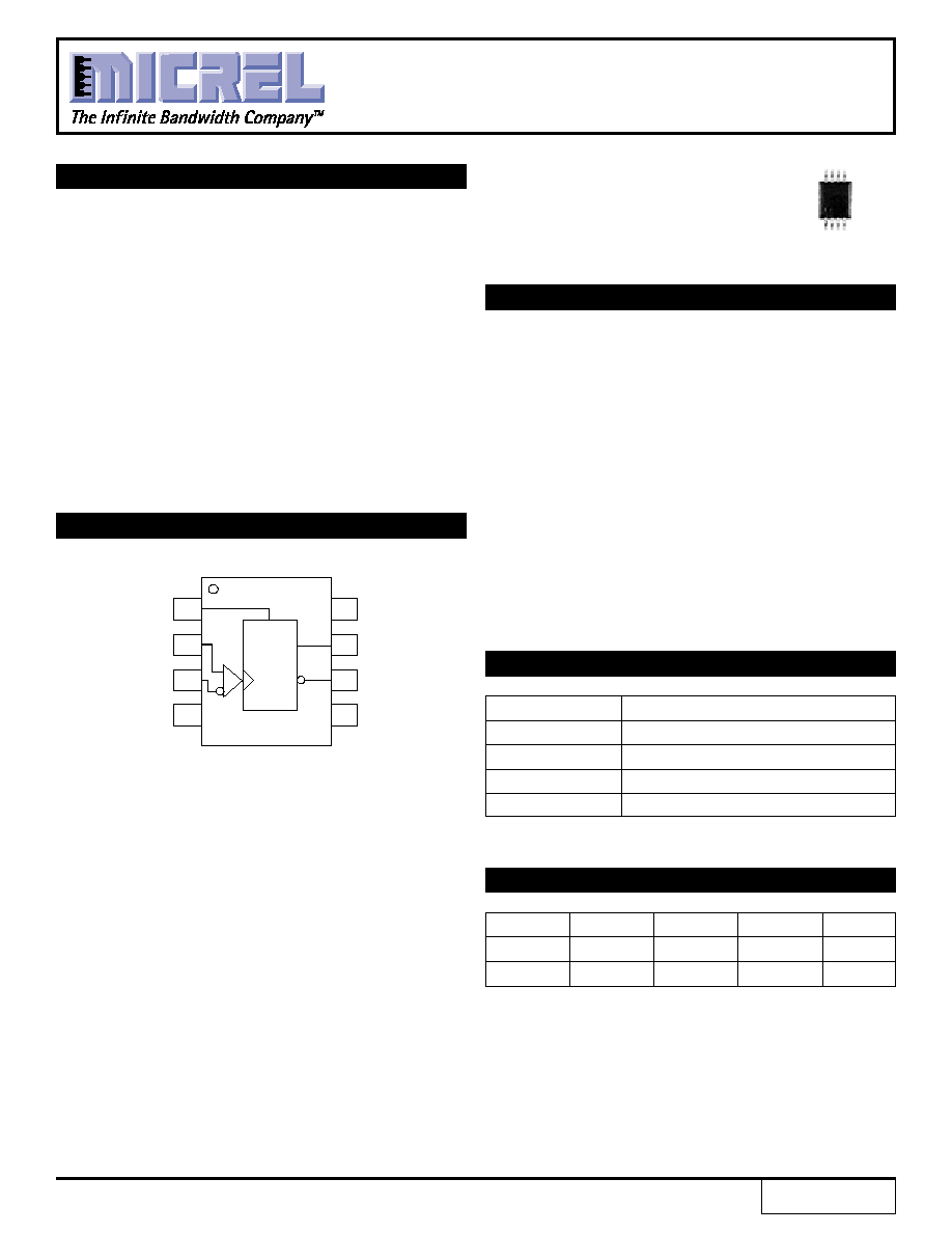
The SY10/100EP32V is an integrated
˜
2 divider with
differential clock inputs.
The V
BB
pin, an internally generated voltage supply,
is available to this device only. For single-ended input
conditions, the unused differential input is connected to
V
BB
as a switching reference voltage. V
BB
may also rebias
AC-coupled inputs. When used, decouple V
BB
and V
CC
via a 0.01
µ
F capacitor and limit current sourcing or sinking
to 0.5mA. When not used, V
BB
should be left open.
The reset pin is asynchronous and is asserted on the
rising edge. Upon power-up, the internal flip-flops will
attain a random state; the reset allows for the
synchronous use of multiple EP32's in a system.
The 100k series includes internal temperature
compensation circuitry.
FEATURES
PIN CONFIGURATION/BLOCK DIAGRAM
PIN NAMES
5V/3.3V
˜
2 DIVIDER
1
2
3
4
5
6
7
8
Reset
VCC
Q
VEE
CLK
VBB
/Q
R
/CLK
˜ 2
TOP VIEW
(Available in MSOP or SOIC package)
Pin
Function
CLK, /CLK
ECL Clock Inputs
Reset
ECL Asynchronous Reset
V
BB
Reference Voltage Output
Q, /Q
ECL Data Outputs
Rev.: C
Amendment: /0
Issue Date:
March 2003
Precision EdgeTM
SY10EP32V
SY100EP32V
FINAL
TRUTH TABLE
(1)
Note 1:
Z = LOW-to-HIGH Transition
/Z = HIGH-to-LOW Transition
F = Divide by 2 function.
ECL ProTM
Precision Edge and ECL Pro are trademarks of Micrel, Inc.
2
Precision EdgeTM
SY10EP32V
SY100EP32V
Micrel
T
A
= ≠40
∞
C
T
A
= +25
∞
C
T
A
= +85
∞
C
Symbol
Parameter
Min.
Typ.
Max.
Min.
Typ.
Max.
Min.
Typ.
Max.
Unit
I
EE
Power Supply Current
--
30
37
--
30
37
--
30
37
mA
V
OH
Output HIGH Voltage
(3)
2165
2290
2415
2230
2355
2480
2290
2415
2540
mV
V
OL
Output LOW Voltage
(3)
1365
1490
1615
1430
1555
1680
1490
1615
1740
mV
V
IH
Input HIGH Voltage
2090
--
2415
2155
--
2480
2215
--
2540
mV
(Single-Ended)
V
IL
Input LOW Voltage
1365
--
1690
1430
--
1755
1490
--
1815
mV
(Single-Ended)
V
BB
Output Voltage
1790
1890
1990
1855
1955
2055
1915
2015
2115
mV
V
IHCMR
Input HIGH Voltage
(4)
Common Mode Range
2.0
--
V
CC
2.0
--
V
CC
2.0
--
V
CC
V
(Differential)
I
IH
Input HIGH Current
--
--
150
--
--
150
--
--
150
µ
A
I
IL
Input LOW Current
CLK
0.5
--
--
0.5
--
--
0.5
--
--
µ
A
/CLK
≠150
--
--
≠150
--
--
≠150
--
--
Note 1.
10EP circuits are designed to meet the DC specifications shown in the above table after thermal equilibrium has been established. The circuit
is in a test socket or mounted on a printed circuit board and traverse airflow greater than 500lfpm is maintained.
Note 2.
Input and output parameters vary 1:1 with V
CC
.
Note 3.
All loading with 50
to V
CC
≠2.0V.
Note 4.
The V
IHCMR
range is referenced to the most positive side of the differential input signal.
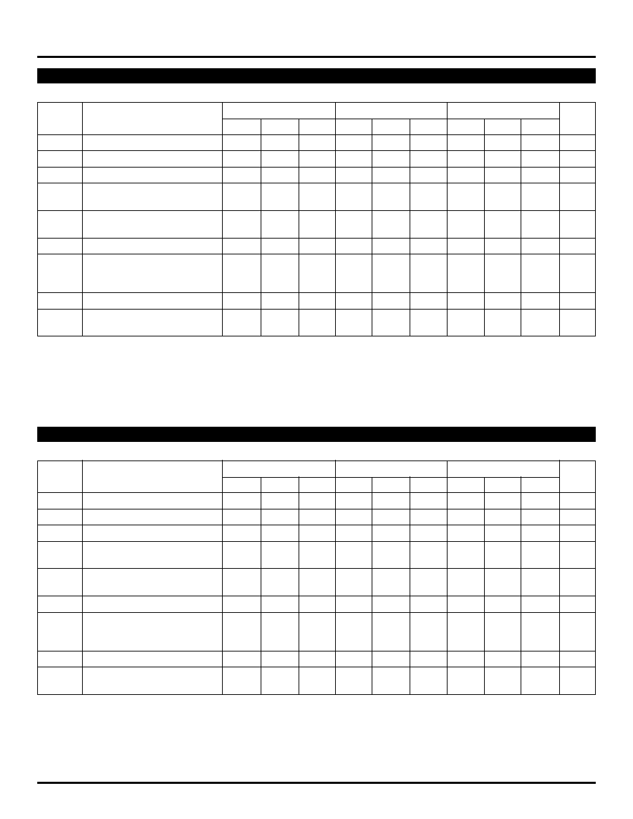
(10EP) LVPECL DC ELECTRICAL CHARACTERISTICS
(1)
V
CC
= 3.3V
±
10%; V
EE
= 0V
(2)
T
A
= ≠40
∞
C
T
A
= +25
∞
C
T
A
= +85
∞
C
Symbol
Parameter
Min.
Typ.
Max.
Min.
Typ.
Max.
Min.
Typ.
Max.
Unit
I
EE
Power Supply Current
--
--
37
--
30
37
--
--
37
mA
V
OH
Output HIGH Voltage
(3)
3865
3990
4115
3930
4055
4180
3990
4115
4240
mV
V
OL
Output LOW Voltage
(3)
3065
3190
3315
3130
3255
3380
3190
3315
3440
mV
V
IH
Input HIGH Voltage
3790
--
4115
3855
--
4180
3915
--
4240
mV
(Single-Ended)
V
IL
Input LOW Voltage
3065
--
3390
3130
--
3455
3190
--
3515
mV
(Single-Ended)
V
BB
Output Voltage
3490
3590
3690
3555
3655
3755
3615
3715
3815
mV
V
IHCMR
Input HIGH Voltage
(4)
Common Mode Range
2.0
--
V
CC
2.0
--
V
CC
2.0
--
V
CC
V
(Differential)
I
IH
Input HIGH Current
--
--
150
--
--
150
--
--
150
µ
A
I
IL
Input LOW Current
CLK
0.5
--
--
0.5
--
--
0.5
--
--
µ
A
/CLK
≠150
--
--
≠150
--
--
≠150
--
--
Note 1.
10EP circuits are designed to meet the DC specifications shown in the above table after thermal equilibrium has been established. The circuit
is in a test socket or mounted on a printed circuit board and traverse airflow greater than 500lfpm is maintained.
Note 2.
Input and output parameters vary 1:1 with V
CC
.
Note 3.
All loading with 50
to V
CC
≠2.0V.
Note 4.
The V
IHCMR
range is referenced to the most positive side of the differential input signal.
(10EP) PECL DC ELECTRICAL CHARACTERISTICS
(1)
V
CC
= 5.0V
±
10%; V
EE
= 0V
(2)
3
Precision EdgeTM
SY10EP32V
SY100EP32V
Micrel
T
A
= ≠40
∞
C
T
A
= +25
∞
C
T
A
= +85
∞
C
Symbol
Parameter
Min.
Typ.
Max.
Min.
Typ.
Max.
Min.
Typ.
Max.
Unit
I
EE
Power Supply Current
--
--
37
--
30
37
--
--
37
mA
V
OH
Output HIGH Voltage
(3)
≠1135
≠1010
≠885
≠1070
≠945
≠820
≠1010
≠885
≠760
mV
V
OL
Output LOW Voltage
(3)
≠1935
≠1810
≠1685
≠1870
≠1745
≠1620
≠1810
≠1685
≠1560
mV
V
IH
Input HIGH Voltage
≠1210
--
≠885
≠1145
--
≠820
≠1085
--
≠760
mV
(Single-Ended)
V
IL
Input LOW Voltage
≠1935
--
≠1610
≠1870
--
≠1545
≠1810
--
≠1485
mV
(Single-Ended)
V
BB
Output Voltage
≠1510
≠1410
≠1310
≠1445
≠1345
≠1245
≠1385
≠1285
≠1185
mV
V
IHCMR
Input HIGH Voltage
(4)
Common Mode Range
V
EE
+2.0
0.0
V
EE
+2.0
0.0
V
EE
+2.0
0.0
V
(Differential)
I
IH
Input HIGH Current
--
--
150
--
--
150
--
--
150
µ
A
I
IL
Input LOW Current
CLK
0.5
--
--
0.5
--
--
0.5
--
--
µ
A
/CLK
≠150
--
--
≠150
--
--
≠150
--
--
Note 1.
10EP circuits are designed to meet the DC specifications shown in the above table after thermal equilibrium has been established. The circuit
is in a test socket or mounted on a printed circuit board and traverse airflow greater than 500lfpm is maintained.
Note 2.
Input and output parameters vary 1:1 with V
CC
.
Note 3.
All loading with 50
to V
CC
≠ 2.0V.
Note 4.
V
IHCMR
(min) varies 1:1 with V
EE
. The V
IHCMR
range is referenced to the most positive side of the differential input signal.
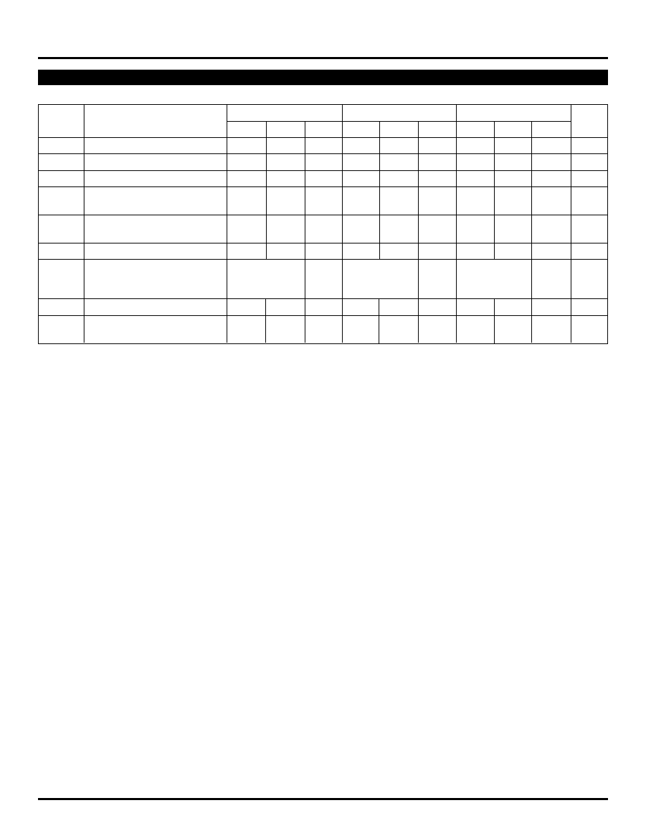
(10EP) ECL/LVECL DC ELECTRICAL CHARACTERISTICS
(1)
V
CC
= 0V; V
EE
= ≠3.3V to 5.0V
±
10%
(2)
4
Precision EdgeTM
SY10EP32V
SY100EP32V
Micrel
T
A
= ≠40
∞
C
T
A
= +25
∞
C
T
A
= +85
∞
C
Symbol
Parameter
Min.
Typ.
Max.
Min.
Typ.
Max.
Min.
Typ.
Max.
Unit
I
EE
Power Supply Current
--
--
37
--
30
37
--
--
42
mA
V
OH
Output HIGH Voltage
(3)
2155
2280
2405
2155
2280
2405
2155
2280
2405
mV
V
OL
Output LOW Voltage
(3)
1355
1480
1605
1355
1480
1605
1355
1480
1605
mV
V
IH
Input HIGH Voltage
2075
--
2420
2075
--
2420
2075
--
2420
mV
(Single-Ended)
V
IL
Input LOW Voltage
1355
--
1675
1355
--
1675
1355
--
1675
mV
(Single-Ended)
V
BB
Output Voltage
1775
1875
1975
1775
1875
1975
1775
1875
1975
mV
V
IHCMR
Input HIGH Voltage
(4)
Common Mode Range
2.0
--
V
CC
2.0
--
V
CC
2.0
--
V
CC
V
(Differential)
I
IH
Input HIGH Current
--
--
150
--
--
150
--
--
150
µ
A
I
IL
Input LOW Current
CLK
0.5
--
--
0.5
--
--
0.5
--
--
µ
A
/CLK
≠150
--
--
≠150
--
--
≠150
--
--
Note 1.
100EP circuits are designed to meet the DC specifications shown in the above table after thermal equilibrium has been established. The circuit
is in a test socket or mounted on a printed circuit board and traverse airflow greater than 500lfpm is maintained.
Note 2.
Input and output parameters vary 1:1 with V
CC
.
Note 3.
All loading with 50
to V
CC
≠2.0V.
Note 4.
The V
IHCMR
range is referenced to the most positive side of the differential input signal.
(100EP) LVPECL DC ELECTRICAL CHARACTERISTICS
(1)
V
CC
= +3.3V
±
10%; V
EE
= 0V
(2)
T
A
= ≠40
∞
C
T
A
= +25
∞
C
T
A
= +85
∞
C
Symbol
Parameter
Min.
Typ.
Max.
Min.
Typ.
Max.
Min.
Typ.
Max.
Unit
I
EE
Power Supply Current
--
--
37
--
30
37
--
--
42
mA
V
OH
Output HIGH Voltage
(3)
3855
3980
4105
3855
3980
4105
3855
3980
4105
mV
V
OL
Output LOW Voltage
(3)
3055
3180
3305
3055
3180
3305
3055
3180
3305
mV
V
IH
Input HIGH Voltage
3775
--
4120
3775
--
4120
3775
--
4120
mV
(Single-Ended)
V
IL
Input LOW Voltage
3055
--
3375
3055
--
3375
3055
--
3375
mV
(Single-Ended)
V
BB
Output Voltage
3475
3575
3675
3475
3575
3675
3475
3575
3675
mV
V
IHCMR
Input HIGH Voltage
(4)
Common Mode Range
2.0
--
V
CC
2.0
--
V
CC
2.0
--
V
CC
V
(Differential)
I
IH
Input HIGH Current
--
--
150
--
--
150
--
--
150
µ
A
I
IL
Input LOW Current
CLK
0.5
--
--
0.5
--
--
0.5
--
--
µ
A
/CLK
≠150
--
--
≠150
--
--
≠150
--
--
Note 1.
100EP circuits are designed to meet the DC specifications shown in the above table after thermal equilibrium has been established. The circuit
is in a test socket or mounted on a printed circuit board and traverse airflow greater than 500lfpm is maintained.
Note 2.
Input and output parameters vary 1:1 with V
CC
.
Note 3.
All loading with 50
to V
CC
≠2.0V.
Note 4.
The V
IHCMR
range is referenced to the most positive side of the differential input signal.
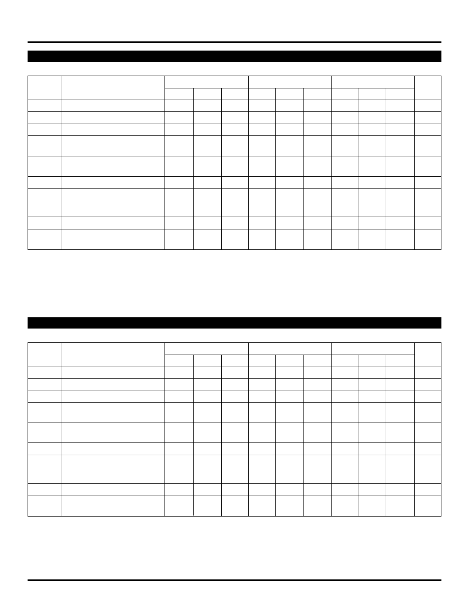
(100EP) PECL DC ELECTRICAL CHARACTERISTICS
(1)
V
CC
= +5.0V
±
10%; V
EE
= 0V
(2)
5
Precision EdgeTM
SY10EP32V
SY100EP32V
Micrel
T
A
= ≠40
∞
C
T
A
= +25
∞
C
T
A
= +85
∞
C
Symbol
Parameter
Min.
Typ.
Max.
Min.
Typ.
Max.
Min.
Typ.
Max.
Unit
I
EE
Power Supply Current
--
--
37
--
30
37
--
--
42
mA
V
OH
Output HIGH Voltage
(3)
≠1145
≠1020
≠895
≠1145
≠1020
≠895
≠1145
≠1020
≠895
mV
V
OL
Output LOW Voltage
(3)
≠1945
≠1820
≠1695
≠1945
≠1820
≠1695
≠1945
≠1820
≠1695
mV
V
IH
Input HIGH Voltage
≠1225
--
≠880
≠1225
--
≠880
≠1225
--
≠880
mV
(Single-Ended)
V
IL
Input LOW Voltage
≠1945
--
≠1625
≠1945
--
≠1625
≠1945
--
≠1625
mV
(Single-Ended)
V
BB
Output Voltage
≠1525
≠1425
≠1325
≠1525
≠1425
≠1325
≠1525
≠1425
≠1325
mV
V
IHCMR
Input HIGH Voltage
(4)
Common Mode Range
V
EE
+2.0
0.0
V
EE
+2.0
0.0
V
EE
+2.0
0.0
V
(Differential)
I
IH
Input HIGH Current
--
--
150
--
--
150
--
--
150
µ
A
I
IL
Input LOW Current
CLK
0.5
--
--
0.5
--
--
0.5
--
--
µ
A
/CLK
≠150
--
--
≠150
--
--
≠150
--
--
Note 1.
100EP circuits are designed to meet the DC specifications shown in the above table after thermal equilibrium has been established. The circuit
is in a test socket or mounted on a printed circuit board and traverse airflow greater than 500lfpm is maintained.
Note 2.
Input and output parameters vary 1:1 with V
CC
.
Note 3.
All loading with 50
to V
CC
≠2.0V.
Note 4.
V
IHCMR
(min) varies 1:1 with V
EE
. The V
IHCMR
range is referenced to the most positive side of the differential input signal.
(100EP) ECL/LVECL DC ELECTRICAL CHARACTERISTICS
(1)
V
CC
= 0V; V
EE
= ≠3.3V to ≠5.0V
±
10%
(2)
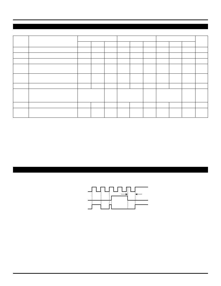
TIMING DIAGRAM
Q
CLK
t
RR
RESET