Pin
Function
Q, /Q
Differential LVPECL Output
D
LVTTL Input
V
CC
Positive Supply
GND
Ground
DESCRIPTION
s
3.3V and 5V power supply options
s
300ps typical propagation delay
s
Differential LVPECL output
s
I
CC
Max 20mA
s
PNP LVTTL input for minimal loading
s
Q output will default HIGH with inputs open
s
High bandwidth to 800MHz typical
s
Available in 8-pin MSOP and SOIC package
The SY10/100EPT20V is a TTL/CMOS to differential
PECL translator. Capable of running from a 3.3 or 5V
supply, the part can be used in either LVTTL/LVCMOS/
LVPECL or TTL/CMOS/PECL systems.
The device only requires a single positive supply of
3.3V or 5V - no negative supply is required.
The tiny 8-pin MSOP package and the low skew, dual
gate design of the EPT20V makes it ideal for those
applications where space, performance, and low power
are at a premium.
FEATURES
5V/3.3V LVTTL/LVCMOS-to-
DIFFERENTIAL LVPECL
TRANSLATOR
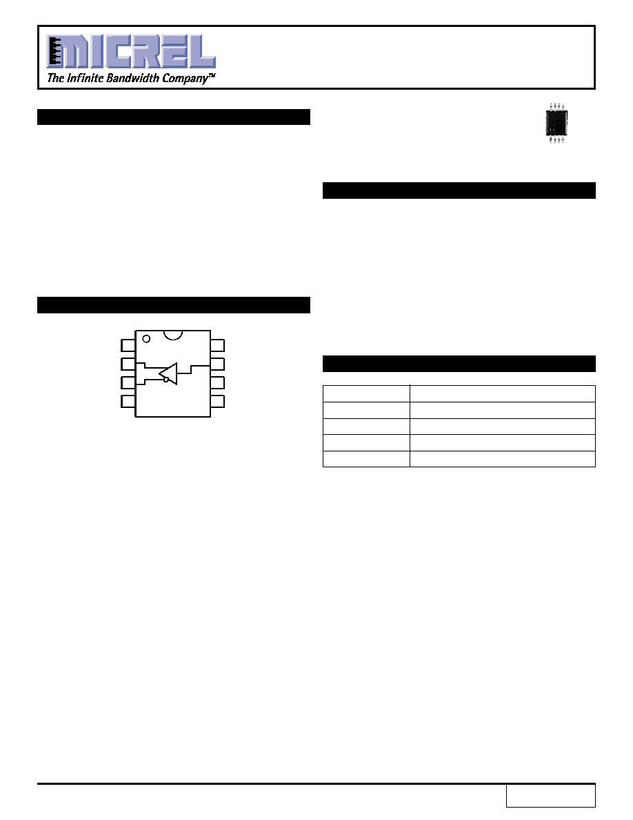
PIN NAMES
PIN CONFIGURATION/BLOCK DIAGRAM
(Available in 8-pin SOIC or 8-pin MSOP)
ECL ProTM
SY10EPT20V
SY100EPT20V
FINAL
1
NC
Q
/Q
NC
8
V
CC
D
NC
GND
7
6
5
2
3
4
LVPECL
LVTTL
1
Rev.: C
Amendment: /0
Issue Date: March 2003
ECL ProTM
ECL Pro is a trademark of Micrel, Inc.

2
ECL ProTM
SY10EPT20V
SY100EPT20V
Micrel
T
A
= ≠40
∞
C
T
A
= 0
∞
C
T
A
= +25
∞
C
T
A
= +85
∞
C
Symbol
Parameter
Min.
Max.
Min.
Max.
Min.
Typ.
Max.
Min.
Max.
Unit
Condition
I
CC
Power Supply Current
--
20
--
20
--
--
20
--
20
mA
--
TRUTH TABLE
D
Q
/Q
H
H
L
L
L
H
Open
H
L
DC ELECTRICAL CHARACTERISTICS
V
CC
= +3.3V
±
10% or +5.0V
±
10%
Symbol
Paramter
Value
Unit
V
CC
Power Supply Voltage
≠0.5 to +7.0
V
V
IN
TTL Input Voltage
≠0.5 to V
CC
V
I
IN
TTL Input Current
≠30 to +5.0
mA
I
OUT
PECL Output Current
mA
≠Continuous
50
≠Surge
100
T
store
Storage Temperature
≠65 to +150
∞
C
T
A
Operating Temperature
≠40 to +85
∞
C
Note 1.
Permanent device damage may occur if ABSOLUTE MAXIMUM
RATINGS are exceeded. This is a stress rating only and
functional operation is not implied at conditions other than those
detailed in the operational sections of this data sheet. Exposure
to ABSOLUTE MAXIMUM RATlNG conditions for extended
periods may affect device reliability.
ABSOLUTE MAXIMUM RATINGS
(1)
T
A
= ≠40
∞
C
T
A
= 0
∞
C
T
A
= +25
∞
C
T
A
= +85
∞
C
Symbol
Parameter
Min.
Max.
Min.
Max.
Min.
Typ.
Max.
Min.
Max.
Unit
Condition
V
IH
Input HIGH Voltage
2.0
--
2.0
--
2.0
--
--
2.0
--
V
--
V
IL
Input LOW Voltage
--
0.8
--
0.8
--
--
0.8
--
0.8
V
--
I
IH
Input HIGH Current
--
20
--
20
--
--
20
--
20
µ
A
V
IN
= 2.7V
--
100
--
100
--
--
100
--
100
V
IN
= V
CC
I
IL
Input LOW Current
--
≠0.2
--
≠0.2
--
--
≠0.2
--
≠0.2
mA
V
IN
= 0.5V
V
IK
Input Clamp Voltage
--
≠1.2
--
≠1.2
--
--
≠1.2
--
≠1.2
V
I
IN
= ≠18mA
TTL DC ELECTRICAL CHARACTERISTICS
V
CC
= +3.3V
±
10% or +5.0V
±
10%
T
A
= ≠40
∞
C
T
A
= 0
∞
C
T
A
= +25
∞
C
T
A
= +85
∞
C
Symbol
Parameter
Min.
Max.
Min.
Max.
Min.
Typ.
Max.
Min.
Max.
Unit
Condition
V
OH
Output HIGH Voltage
(1)
mV
10EPT
3920
4110
3980
4160
4020
--
4190
4090
4280
100EPT
3915
4120
3975
4120
3975
--
4120
3975
4120
V
OL
Output LOW Voltage
(1)
mV
10EPT
3050
3350
3050
3370
3050
--
3370
3050
3405
100EPT
3170
3445
3190
3380
3190
--
3380
3190
3380
Note 1.
These values are for V
CC
= 5.0V. Level Specifications will vary 1:1 with V
CC
.
PECL DC ELECTRICAL CHARACTERISTICS
V
CC
= +3.3V
±
10% or +5.0V
±
10%

3
ECL ProTM
SY10EPT20V
SY100EPT20V
Micrel
PRODUCT ORDERING INFORMATION
Ordering
Package
Operating
Marking
Code
Type
Range
Code
SY10EPT20VZC
Z8-1
Commercial
HEP20
SY10EPT20VZCTR
(1)
Z8-1
Commercial
HEP20
SY100EPT20VZC
Z8-1
Commercial
XEP20
SY100EPT20VZCTR
(1)
Z8-1
Commercial
XEP20
SY10EPT20VKC
K8-1
Commercial
HP20
SY10EPT20VKCTR
(1)
K8-1
Commercial
HP20
SY100EPT20VKC
K8-1
Commercial
XP20
SY100EPT20VKCTR
(1)
K8-1
Commercial
XP20
Note 1.
Tape and Reel.
Note 2.
Recommended for new designs.
T
A
= ≠40
∞
C
T
A
= 0
∞
C
T
A
= +25
∞
C
T
A
= +85
∞
C
Symbol
Parameter
Min.
Max.
Min.
Max.
Min.
Typ.
Max.
Min.
Max. Unit
Condition
t
PLH
Propagation Delay
(1)
100
600
100
600
100
--
600
100
600
ps
50
to V
CC
≠ 2.0V
t
PHL
t
skpp
Part-to-Part Skew
(2)
--
500
--
500
--
--
500
--
500
ps
50
to V
CC
≠ 2.0V
f
MAX
Maximum Input Frequency
350
--
350
--
350
--
--
350
--
MHz
50
to V
CC
≠ 2.0V
f
MAX
Maximum Toggle Frequency
--
800
--
800
--
--
800
--
800
MHz
50
to V
CC
≠ 2.0V
t
r
Output Rise/Fall Time
200
500
200
500
200
--
500
200
500
ps
50
to V
CC
≠ 2.0V
t
f
(20% to 80%)
AC ELECTRICAL CHARACTERISTICS
(1)
V
CC
= +3.3V
±
10% or +5.0V
±
10%
Note 1.
Input Rise Time < 1.0ns.
Note 2.
Guaranteed by design. Not tested in production.
Ordering
Package
Operating
Marking
Code
Type
Range
Code
SY10EPT20VZI
(2)
Z8-1
Industrial
HEP20
SY10EPT20VZITR
(1,2)
Z8-1
Industrial
HEP20
SY100EPT20VZI
(2)
Z8-1
Industrial
XEP20
SY100EPT20VZITR
(1,2)
Z8-1
Industrial
XEP20
SY10EPT20VKI
(2)
K8-1
Industrial
HP20
SY10EPT20VKITR
(1,2)
K8-1
Industrial
HP20
SY100EPT20VKI
(2)
K8-1
Industrial
XP20
SY100EPT20VKITR
(1,2)
K8-1
Industrial
XP20

5
ECL ProTM
SY10EPT20V
SY100EPT20V
Micrel
8 LEAD MSOP (K8-1)
Rev. 01
MICREL, INC.
1849 FORTUNE DRIVE
SAN JOSE, CA 95131
USA
TEL
+ 1 (408) 944-0800
FAX
+ 1 (408) 944-0970
WEB
http://www.micrel.com
The information furnished by Micrel in this datasheet is believed to be accurate and reliable. However, no responsibility is assumed by Micrel for its use.
Micrel reserves the right to change circuitry and specifications at any time without notification to the customer.
Micrel Products are not designed or authorized for use as components in life support appliances, devices or systems where malfunction of a product can
reasonably be expected to result in personal injury. Life support devices or systems are devices or systems that (a) are intended for surgical implant into
the body or (b) support or sustain life, and whose failure to perform can be reasonably expected to result in a significant injury to the user. A Purchaser's
use or sale of Micrel Products for use in life support appliances, devices or systems is at Purchaser's own risk and Purchaser agrees to fully indemnify
Micrel for any damages resulting from such use or sale.
© 2003 Micrel, Incorporated.
