DESCRIPTION
s
275ps propagation delay
s
High bandwidth output transitions
s
Internal 75K
input pull-down resistors
s
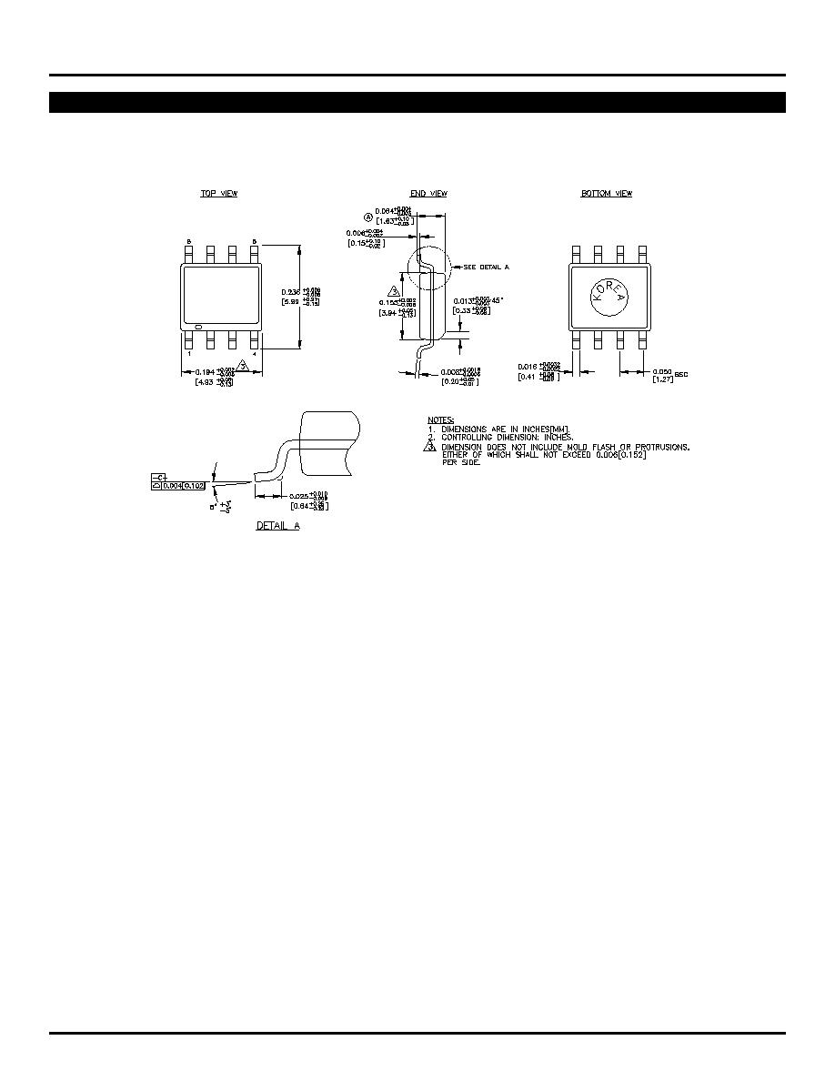
Available in 8-pin SOIC package
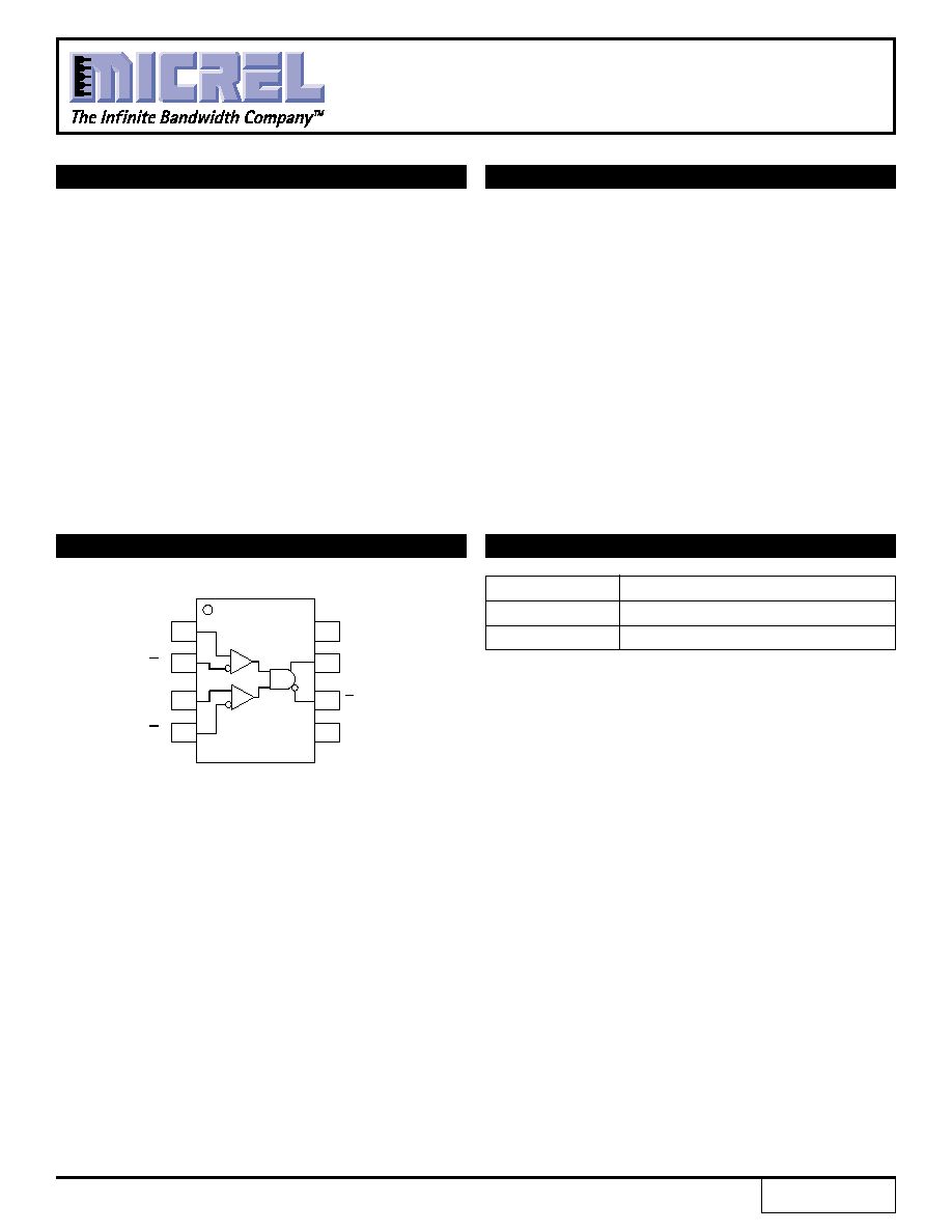
The SY10/100EL05 are 2-input differential AND/NAND
gates. These devices are functionally equivalent to the
E404 devices, with higher performance capabilities. With
propagation delays and output transition times
significantly faster than the E404, the EL05 is ideally
suited for those applications which require the ultimate
in AC performance.
Because a negative 2-input NAND is equivalent to a
2-input OR function with inverted inputs, the differential
inputs and outputs of the device allows the EL05 to also
be used as a 2-input differential OR/NOR gate.
The differential inputs employ clamp circuitry so that,
under open conditions (pulled down to V
EE
), the input to
the AND gate will be HIGH. In this way, if one set of
inputs is open, the gate will remain active to the other
input.
FEATURES
2-INPUT
DIFFERENTIAL
AND/NAND
PIN CONFIGURATION/BLOCK DIAGRAM
Pin
Function
D
0
, D
1
Data Inputs
Q
Data Outputs
Rev.: E
Amendment: /0
Issue Date:
August, 1998
SY10EL05
SY100EL05
PIN NAMES
1
2
3
4
5
6
7
8
D
0
D
1
V
CC
Q
V
EE
Q
D
0
D
1
1
SOIC
TOP VIEW
2
SY10EL05
SY100EL05
Micrel
T
A
= ≠40
∞
C
T
A
= 0
∞
C
T
A
= +25
∞
C
T
A
= +85
∞
C
Symbol
Parameter
Min.
Typ.
Max.
Min.
Typ.
Max.
Min.
Typ.
Max.
Min.
Typ.
Max.
Unit
t
PLH
Propagation Delay to
135
260
440
185
275
390
185
275
390
215
305
420
ps
t
PHL
Output D
V
PP
Minimum Input Swing
(1)
150
--
--
150
--
--
150
--
--
150
--
--
mV
V
CMR
Common Mode Range
(2)
(2)
--
≠0.4
(2)
--
≠0.4
(2)
--
≠0.4
(2)
--
≠0.4
V
t
r
Output Rise/Fall Times Q
100
225
350
100
225
350
100
225
350
100
225
350
ps
t
f
(20% to 80%)
AC ELECTRICAL CHARACTERISTICS
V
EE
= V
EE
(Min.) to V
EE
(Max.); V
CC
= GND
NOTES:
1. Minimum input swing for which AC parameters are guaranteed. The device has a DC gain of
40.
2. The CMR range is referenced to the most positive side of the differential input signal. Normal operation is obtained if the HIGH level falls within the specified
range and the peak-to-peak voltage lies between V
PP
min. and 1V. The lower end of the CMR range is dependent on V
EE
and is equal to V
EE
+ 3.0V.
PRODUCT ORDERING CODE
DC ELECTRICAL CHARACTERISTICS
T
A
= ≠40
∞
C
T
A
= 0
∞
C
T
A
= +25
∞
C
T
A
= +85
∞
C
Symbol
Parameter
Min.
Typ.
Max.
Min.
Typ.
Max.
Min.
Typ.
Max.
Min.
Typ.
Max.
Unit
I
EE
Power Supply Current
mA
10EL
--
18
22
14
18
22
14
18
22
14
18
22
100EL
--
18
22
14
18
22
14
18
22
16
21
25
V
EE
Power Supply Voltage
V
10EL ≠4.75
≠5.2
≠5.5
≠4.75
≠5.2
≠5.5
≠4.75
≠5.2
≠5.5
≠4.75
≠5.2
≠5.5
100EL ≠4.20
≠4.5
≠5.5
≠4.20
≠4.5
≠5.5
≠4.20
≠4.5
≠5.5
≠4.20
≠4.5
≠5.5
I
IH
Input HIGH Current
--
--
150
--
--
150
--
--
150
--
--
150
µ
A
V
EE
= V
EE
(Min.) to V
EE
(Max.); V
CC
= GND
Ordering
Package
Operating
Code
Type
Range
SY10EL05ZC
Z8-1
Commercial
SY10EL05ZCTR
Z8-1
Commercial
SY100EL05ZC
Z8-1
Commercial
SY100EL05ZCTR
Z8-1
Commercial

4
SY10EL05
SY100EL05
Micrel
MICREL-SYNERGY
3250 SCOTT BOULEVARD
SANTA CLARA
CA 95054
USA
TEL
+ 1 (408) 980-9191
FAX
+ 1 (408) 914-7878
WEB
http://www.micrel.com
This information is believed to be accurate and reliable, however no responsibility is assumed by Micrel for its use nor for any infringement of patents or
other rights of third parties resulting from its use. No license is granted by implication or otherwise under any patent or patent right of Micrel Inc.
© 2000 Micrel Incorporated