The SY10/100EL34/L are low skew
˜
2,
˜
4,
˜
8 clock
generation chips designed explicitly for low skew clock
generation applications. The internal dividers are
synchronous to each other, therefore, the common output
edges are all precisely aligned. The devices can be driven
by either a differential or single-ended ECL or, if positive
power supplies are used, PECL input signal. In addition,
by using the V
BB
output, a sinusoidal source can be AC-
coupled into the device. If a single-ended input is to be
used, the V
BB
output should be connected to the CLK
input and bypassed to ground via a 0.01
µ
F capacitor.
The V
BB
output is designed to act as the switching
reference for the input of the EL34/L under single-ended
input conditions. As a result, this pin can only source/
sink up to 0.5mA of current.
The common enable (EN) is synchronous so that the
internal dividers will only be enabled/disabled when the
internal clock is already in the LOW state. This avoids
any chance of generating a runt clock pulse on the
internal clock when the device is enabled/disabled as
can happen with an asynchronous control. An internal
runt pulse could lead to losing synchronization between
the internal divider stages. The internal enable flip-flop is
clocked on the falling edge of the divider stages. The
internal enable flip-flop is clocked on the falling edge of
the input clock, therefore, all associated specification
limits are referenced to the negative edge of the clock
input.
Upon start-up, the internal flip-flops will attain a random
state; the master reset (MR) input allows for the
synchronization of the internal dividers, as well as for
multiple EL34/Ls in a system.
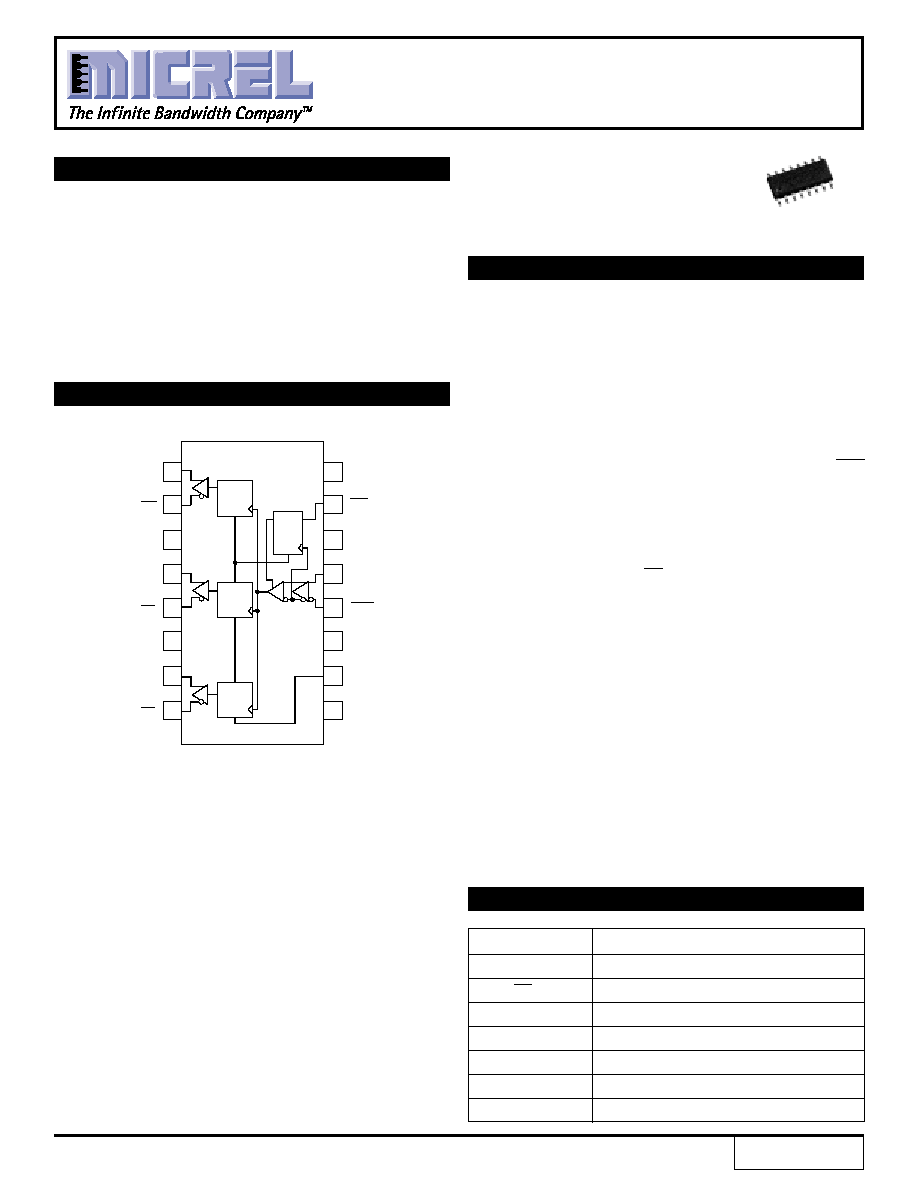
Pin
Function
CLK
Differential Clock Inputs
EN
Synchronous Enable
MR
Master Reset
V
BB
Reference Output
Q
0
Differential
˜
2 Outputs
Q
1
Differential
˜
4 Outputs
Q
2
Differential
˜
8 Outputs
DESCRIPTION
PIN NAMES
FEATURES
5V/3.3V
˜
2,
˜
4,
˜
8 CLOCK
GENERATION CHIP
Precision EdgeTM
SY10EL34/L
SY100EL34/L
FINAL
PIN CONFIGURATION/BLOCK DIAGRAM
SOIC
TOP VIEW
s
3.3V and 5V power supply options
s
50ps output-to-output skew
s
Synchronous enable/disable
s
Master Reset for synchronization
s
Internal 75K
input pull-down resistors
s
Available in 16-pin SOIC package
V
CC
EN
NC
CLK
CLK
V
BB
MR
V
EE
Q
0
Q
0
V
CC
Q
1
Q
1
V
CC
Q
2
Q
2
16
15
14
13
12
11
10
9
1
2
3
4
5
6
7
8
R
Q
˜2
Q
R
˜4
Q
˜8
R
Q D
R
1
Rev.: G
Amendment: /0
Issue Date:
February 2003
Precision Edge is a trademark of Micrel, Inc.
Precision EdgeTM
2
Precision EdgeTM
SY10EL34/L
SY100EL34/L
Micrel
T
A =
≠40
∞
C
T
A =
0
∞
C
T
A =
+25
∞
C
T
A =
+85
∞
C
Symbol
Parameter
Min.
Typ.
Max.
Min.
Typ.
Max.
Min.
Typ.
Max.
Min.
Typ.
Max.
Unit
I
EE
Power Supply
10EL
--
--
49
--
--
49
--
--
49
--
--
49
mA
Current
100EL
--
--
49
--
--
49
--
--
49
--
--
54
V
BB
Output Reference 10EL ≠1.43
--
≠1.30 ≠1.38
--
≠1.27 ≠1.35
--
≠1.25 ≠1.31
--
≠1.19
V
Voltage
100EL ≠1.38
--
≠1.26 ≠1.38
--
≠1.26 ≠1.38
--
≠1.26 ≠1.38
--
≠1.26
I
IH
Input High Current
--
--
150
--
--
150
--
--
150
--
--
150
µ
A
DC ELECTRICAL CHARACTERISTICS
(1)
V
EE
= V
EE
(Min.) to V
EE
(Max.); V
CC
= GND
NOTE:
1. Parametric values specified at:
5 volt Power Supply Range
100EL34 Series:
-4.2V to -5.5V.
10EL34 Series
-4.75V to -5.5V.
3 volt Power Supply Range
10/100EL34L Series:
-3.0V to -3.8V.
T
A =
≠40
∞
C
T
A =
0
∞
C
T
A =
+25
∞
C
T
A =
+85
∞
C
Symbol
Parameter
Min.
Typ.
Max.
Min.
Typ.
Max.
Min.
Typ.
Max.
Min.
Typ.
Max.
Unit
t
PLH
Propagation Delay to
ps
t
PHL
Output
CLK
960
1100
1200
960
1100
1200
960
1100
1200
960
1100 1200
MR
650
800
1010
650
800
1010
650
800
1010
650
800
1010
t
skew
Within-Device Skew
(2)
--
--
50
--
--
50
--
--
50
--
--
50
ps
t
S
Set-up Time EN
400
--
--
400
--
--
400
--
--
400
--
--
ps
t
H
Hold Time EN
200
--
--
200
--
--
200
--
--
200
--
--
ps
V
PP
Minimum Input Swing
(3)
250
--
--
250
--
--
250
--
--
250
--
--
mV
V
CMR
Common Mode Range
(4)
≠1.3
--
≠0.4
≠1.4
--
≠0.4
≠1.4
--
≠0.4
≠1.4
--
≠0.4
V
t
r
Output Rise/Fall Times
275
400
525
275
400
525
275
400
525
275
400
525
ps
t
f
Q (20% ≠ 80%)
V
EE
= V
EE
(Min.) to V
EE
(Max.); V
CC
= GND
AC ELECTRICAL CHARACTERISTICS
(1)
NOTES:
1. Parametric values specified at:
5 volt Power Supply Range
100EL34 Series:
-4.2V to -5.5V.
10EL34 Series
-4.75V to -5.5V.
3 volt Power Supply Range
10/100EL34L Series:
-3.0V to -3.8V.
2. Skew is measured between outputs under identical transitions.
3. Minimum input swing for which AC parameters are guaranteed. The device will function reliably with differential inputs down to 100mV.
4. The CMR range is referenced to the most positive side of the differential input signal. Normal operation is obtained if the HIGH level falls within the specified
range and the peak-to-peak voltage lies between V
PP
min. and 1V. The lower end of the CMR range varies 1:1 with V
EE
. The numbers in the spec table
assume a nominal V
EE
= ≠3.3V. Note for PECL operation, the V
CMR
(min) will be fixed at 3.3V ≠ IV
CMR
(min)I.
TRUTH TABLE
CLK
EN
MR
Function
Z
L
L
Divide
ZZ
H
L
Hold Q
0≠2
X
X
H
Reset Q
0≠2
NOTE:
Z = LOW-to-HIGH transition
ZZ = HIGH-to-LOW transition
3
Precision EdgeTM
SY10EL34/L
SY100EL34/L
Micrel
Ordering
Package
Operating
Marking
Code
Type
Range
Code
SY10EL34LZC
Z16-2
Commercial
HEL34L
SY10EL34LZCTR*
Z16-2
Commercial
HEL34L
SY100EL34LZC
Z16-2
Commercial
XEL34L
SY100EL34LZCTR*
Z16-2
Commercial
XEL34L
*Tape and Reel
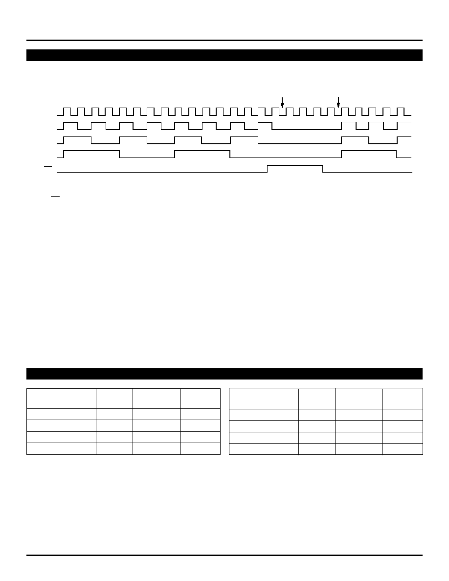
TIMING DIAGRAM
The EN signal will freeze the internal clocks to the flip-flops on the first falling edge of CLK after its assertion. The internal dividers
will maintain their state during the internal clock freeze and will return to clocking once the internal clocks are unfrozen. The outputs
will transition to their next states in the same manner, time and relationship as they would have had the EN signal not been asserted.
PRODUCT ORDERING CODE
EN
Q1
Q2
CLK
Internal Clock
Disabled
Internal Clock
Enabled
Q0
Note 1.
Recommended for new designs.
Ordering
Package
Operating
Marking
Code
Type
Range
Code
SY10EL34LZI
(1)
Z16-2
Industrial
HEL34L
SY10EL34LZITR*
(1)
Z16-2
Industrial
HEL34L
SY100EL34LZI
(1)
Z16-2
Industrial
XEL34L
SY100EL34LZITR*
(1)
Z16-2
Industrial
XEL34L
*Tape and Reel
4
Precision EdgeTM
SY10EL34/L
SY100EL34/L
Micrel
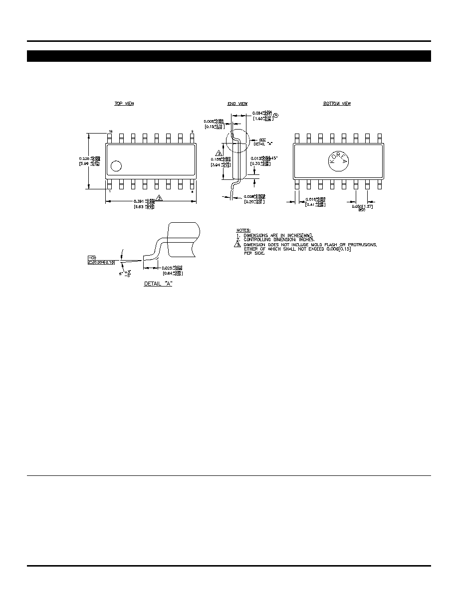
16 LEAD SOIC .150" WIDE (Z16-2)
Rev. 02
MICREL, INC.
1849 FORTUNE DRIVE
SAN JOSE, CA 95131
USA
TEL
+ 1 (408) 944-0800
FAX
+ 1 (408) 944-0970
WEB
http://www.micrel.com
The information furnished by Micrel in this datasheet is believed to be accurate and reliable. However, no responsibility is assumed by Micrel for its use.
Micrel reserves the right to change circuitry and specifications at any time without notification to the customer.
Micrel Products are not designed or authorized for use as components in life support appliances, devices or systems where malfunction of a product can
reasonably be expected to result in personal injury. Life support devices or systems are devices or systems that (a) are intended for surgical implant into
the body or (b) support or sustain life, and whose failure to perform can be reasonably expected to result in a significant injury to the user. A Purchaser's
use or sale of Micrel Products for use in life support appliances, devices or systems is at Purchaser's own risk and Purchaser agrees to fully indemnify
Micrel for any damages resulting from such use or sale.
© 2003 Micrel, Incorporated.