1
ECL ProTM
SY10EP51V
Micrel
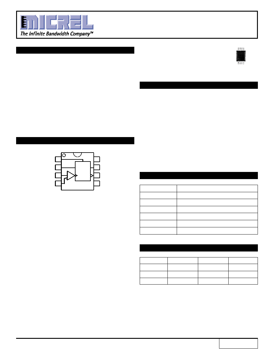
Pin
Function
CLK, /CLK
ECL Clock Inputs
RESET
ECL Asynchronous Reset
D
ECL Data Input
Q, /Q
ECL Data Outputs
V
CC
Positive Supply
V
EE
Negative, 0 Supply
DESCRIPTION
s
3.3V and 5V power supply options
s
320ps typical propagation delay
s
Maximum frequency > 3GHz typical
s
75
internal input pulldown resistor
s
Transistor count: 143
s
Available in 8-Pin (3mm) MSOP and SOIC packages
The SY10EP51V is a D flip-flop with reset and
differential clock. The device is pin and functionally
equivalent to the EL51 device.
The reset input is an asynchronous, level triggered
signal. Data enters the master portion of the flip-flop
when CLK is LOW and is transferred to the slave, and
thus the outputs, upon a positive transition of the CLK.
The differential clock inputs of the EP51V allow the device
to be used as a negative edge triggered flip-flop.
The differential input employs clamp circuitry to
maintain stability under open input conditions. When left
open, the CLK input will be pulled down to V
EE
and the
/CLK input will be biased a V
CC
/2.
FEATURES
5V/3.3V D FLIP-FLOP
WITH RESET AND
DIFFERENTIAL CLOCK
PIN NAMES
PIN CONFIGURATION/BLOCK DIAGRAM
ECL ProTM
SY10EP51V
FINAL
Rev.: C
Amendment: /0
Issue Date:
March 2003
1
RESET
D
CLK
/CLK
8
VCC
Q
/Q
VEE
7
6
5
2
3
4
Flip
Flop
D
R
Available in 8-Pin SOIC and MSOP Packages
TRUTH TABLE
D
RESET
CLK
Q
L
L
Z
L
H
L
Z
H
X
H
X
L
Z = LOW to HIGH Transition
ECL ProTM
ECL Pro is a trademark of Micrel, Inc.

2
ECL ProTM
SY10EP51V
Micrel
Symbol
Rating
Value
Unit
V
CC
-- V
EE
Power Supply Voltage
6V
V
V
IN
Input Voltage (V
CC
= 0V, V
IN
not more negative than V
EE
)
�6.0 to 0
V
Input Voltage (V
EE
= 0V, V
IN
not more positive than V
CC
)
+6.0 to 0
V
I
OUT
Output Current
�Continuous
50
mA
�Surge
100
T
A
Operating Temperature Range
�40 to +85
�
C
T
store
Storage Temperature Range
�65 to +150
�
C
JA
Package Thermal Resistance
�Still-Air
(SOIC)
160
�
C/W
(Junction-to-Ambient)
�500lfpm (SOIC)
109
�Still-Air
(MSOP)
206
�
C/W
�500lfpm (MSOP)
155
JC
Package Thermal Resistance
(SOIC)
39
�
C/W
(Junction-to-Case)
(MSOP)
39
Note 1.
Permanent device damage may occur if ABSOLUTE MAXIMUM RATINGS are exceeded. This is a stress rating only and functional operation
is not implied at conditions other than those detailed in the operational sections of this data sheet. Exposure to ABSOLUTE MAXIMUM
RATlNG conditions for extended periods may affect device reliability.
ABSOLUTE MAXIMUM RATINGS
(1)
T
A
= �40
�
C
T
A
= +25
�
C
T
A
= +85
�
C
Symbol
Parameter
Min.
Typ.
Max.
Min.
Typ.
Max.
Min.
Typ.
Max.
Unit
I
EE
Power Supply Current
(3)
--
35
40
--
35
40
--
35
40
mA
V
OH
Output HIGH Voltage
(4)
3865
3990
4115
3930
4055
4180
3990
4115
4240
mV
V
OL
Outuput LOW Voltage
(4)
3050
3190
3315
3050
3255
3380
3050
3315
3440
mV
V
IH
Input HIGH Voltage
3790
--
4115
3855
--
4180
3915
--
4240
mV
(Single-Ended)
V
IL
Input LOW Voltage
3065
--
3390
3130
--
3455
3190
--
3515
mV
(Single-Ended)
V
IHCMR
Input HIGH Voltage
(5)
2.0
--
V
CC
2.0
--
V
CC
2.0
--
V
CC
V
Common Mode Range
I
IH
Input HIGH Current
--
--
150
--
--
150
--
--
150
�
A
I
IL
Input LOW Current
0.5
--
--
0.5
--
--
0.5
--
--
�
A
Note 1.
10EP circuits are designed to meet the DC specifications shown in the above table after thermal equilibrium has been established. The circuit
is in a test socket or mounted on a printed circuit board and traverse airflow greater than 500lfpm is maintained.
Note 2.
Input and output parameters vary 1:1 with V
CC
. V
CC
can vary +0.25V to +0.5V.
Note 3.
V
CC
= 0V, V
EE
= V
EE
(min.) to V
EE
(max.), all other pins floating.
Note 4.
All loading with 50
to V
CC
�2.0V.
Note 5.
V
IHCMR
(min) varies 1:1 with V
EE
, V
IHCMR
(max) varies 1:1 with V
CC
. The V
IHCMR
range is referenced to the most positive side of the differential
input signal.
5V PECL DC ELECTRICAL CHARACTERISTICS
(1)
V
CC
= 5.0V, V
EE
= 0V
(2)

3
ECL ProTM
SY10EP51V
Micrel
T
A
= �40
�
C
T
A
= +25
�
C
T
A
= +85
�
C
Symbol
Parameter
Min.
Typ.
Max.
Min.
Typ.
Max.
Min.
Typ.
Max.
Unit
I
EE
Power Supply Current
(3)
--
35
40
--
35
40
--
35
40
mA
V
OH
Output HIGH Voltage
(4)
2165
2290
2415
2230
2355
2480
2290
2415
2540
mV
V
OL
Outuput LOW Voltage
(4)
1350
1490
1615
1350
1555
1680
1350
1615
1740
mV
V
IH
Input HIGH Voltage
2090
--
2415
2155
--
2480
2215
--
2540
mV
(Single-Ended)
V
IL
Input LOW Voltage
1365
--
1690
1430
--
1755
1490
--
1815
mV
(Single-Ended)
V
IHCMR
Input HIGH Voltage
(5)
2.0
--
V
CC
2.0
--
V
CC
2.0
--
V
CC
V
Common Mode Range (Diff.)
I
IH
Input HIGH Current
--
--
150
--
--
150
--
--
150
�
A
I
IL
Input LOW Current
0.5
--
--
0.5
--
--
0.5
--
--
�
A
Note 1.
10EP circuits are designed to meet the DC specifications shown in the above table after thermal equilibrium has been established. The circuit
is in a test socket or mounted on a printed circuit board and traverse airflow greater than 500lfpm is maintained.
Note 2.
Input and output parameters vary 1:1 with V
CC
. V
CC
can vary �0.3V to +0.5V.
Note 3.
V
CC
= 0V, V
EE
= V
EE
(min.) to V
EE
(max.), all other pins floating.
Note 4.
All loading with 50
to V
CC
�2.0V.
Note 5.
V
IHCMR
(min) varies 1:1 with V
EE
, V
IHCMR
(max) varies 1:1 with V
CC
. The V
IHCMR
range is referenced to the most positive side of the differential
input signal.
3.3V LVPECL DC ELECTRICAL CHARACTERISTICS
(1)
V
CC
= 3.3V, V
EE
= 0V
(2)
T
A
= �40
�
C
T
A
= +25
�
C
T
A
= +85
�
C
Symbol
Parameter
Min.
Typ.
Max.
Min.
Typ.
Max.
Min.
Typ.
Max.
Unit
I
EE
Power Supply Current
(2)
--
35
40
--
35
40
--
35
40
mA
V
OH
Output HIGH Voltage
(3)
�1135
�1010
�0885
�1070
�0945
�0820
�1010
�0885
�0760
mV
V
OL
Outuput LOW Voltage
(3)
�1950
�1810
�1685
�1950
�1745
�1620
�1950
�1685
�1560
mV
V
IH
Input HIGH Voltage
�1210
--
�0885
�1145
--
�0820
�1085
--
�0760
mV
V
IL
Input LOW Voltage
�1935
--
�1610
�1870
--
�1545
�1810
--
�1485
mV
V
IHCMR
Input HIGH Voltage
V
EE
+2.0
0.0
V
EE
+2.0
0.0
V
EE
+2.0
0.0
V
Common Mode Range
(4)
I
IH
Input HIGH Current
--
--
150
--
--
150
--
--
150
�
A
I
IL
Input LOW Current
0.5
--
--
0.5
--
--
0.5
--
--
�
A
Note 1.
10EP circuits are designed to meet the DC specifications shown in the above table after thermal equilibrium has been established. The circuit
is in a test socket or mounted on a printed circuit board and traverse airflow greater than 500lfpm is maintained.
Note 2.
V
CC
= 0V, V
EE
= V
EE
(min) to V
EE
(max), all other pins floating.
Note 3.
All loading with 50
to V
CC
�2.0V.
Note 4.
V
IHCMR
min varies 1:1 with V
EE
, max varies 1:1 with V
CC
.
NECL/LVECL DC ELECTRICAL CHARACTERISTICS
(1)
V
CC
= 0V, V
EE
= �5.5V to �3.0V
4
ECL ProTM
SY10EP51V
Micrel
T
A
= �40
�
C
T
A
= +25
�
C
T
A
= +85
�
C
Symbol
Parameter
Min.
Typ.
Max.
Min.
Typ.
Max.
Min.
Typ.
Max.
Unit
f
MAX
Maximum Toggle Frequency
(2)
3
--
--
3
--
--
3
--
--
GHz
t
PLH
Propagation Delay to Output
ps
t
PHL
Differential CLK, /CLK
Q, /Q
250
300
350
270
320
370
300
350
420
RESET
Q, /Q
260
310
450
210
320
475
280
320
500
t
RR
Reset Recovery
150
--
--
150
--
--
150
--
--
ps
t
S
Setup Time
100
--
--
100
80
--
100
--
--
ps
t
H
Hold Time
100
--
--
100
40
--
100
--
--
ps
t
PW
Minimum Pulse Width RESET
500
440
--
500
440
--
500
440
--
ps
t
r
Output Rise/Fall Times
Q, /Q
70
120
170
80
130
180
100
150
200
ps
t
f
(20% to 80%)
Note 1.
Measured using 750mV source, 50% duty cycle clock source. All loading with 50
to V
CC
�2.0V.
Note 2.
f
MAX
guaranteed for functionality only. V
OL
and V
OH
levels are guaranteed at DC only.
AC ELECTRICAL CHARACTERISTICS
V
CC
= 0V, V
EE
= �3.0V to �5.5V; V
CC
= 3.0V to 5.5V, V
EE
= 0V
(1)
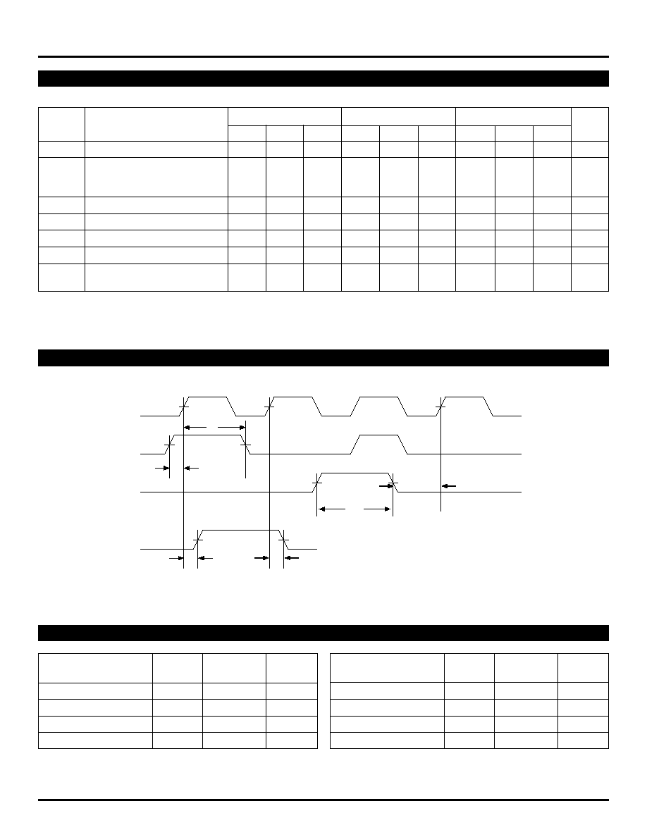
CLK
DATA
RESET
Q
50%
tH
50%
tS
tRR
tPLH
50%
50%
tPHL
tPW
TIMING DIAGRAMS
PRODUCT ORDERING CODE
Ordering
Package
Operating
Package
Code
Type
Range
Marking
SY10EP51VKC
K8-1
Commercial
HP51
SY10EP51VKCTR
(1)
K8-1
Commercial
HP51
SY10EP51VZC
Z8-1
Commercial
HEP51V
SY10EP51VZCTR
(1)
Z8-1
Commercial
HEP51V
Note 1.
Tape and Reel.
Note 2.
Recommended for new designs.
Ordering
Package
Operating
Package
Code
Type
Range
Marking
SY10EP51VKC
(2)
K8-1
Industrial
HP51
SY10EP51VKCTR
(1,2)
K8-1
Industrial
HP51
SY10EP51VZC
(2)
Z8-1
Industrial
HEP51V
SY10EP51VZCTR
(1,2)
Z8-1
Industrial
HEP51V

5
ECL ProTM
SY10EP51V
Micrel
8 LEAD MSOP (K8-1)
Rev. 01