
1
ECL ProTM
SY10EP53V
Micrel
DESCRIPTION
s
3.3V and 5V power supply options
s
3.0GHz toggle frequency
s
75K
internal input pulldown resistors
s
Available in 10-pin MSOP package
The SY10EP53V is a differential data, differential clock
D flip-flop with set and reset. The EP53V is ideally suited
for those applications which require the ultimate in AC
performance.
Data enters the master portion of the flip-flop when
the clock is LOW and is transferred to the slave, and
thus the outputs, upon a positive transition of the clock.
The differential clock inputs also allow the EP53V to be
used as a negative edge triggered device. Both set and
reset inputs are asynchronous, level triggered signals.
The EP53V employs input clamping circuitry so that,
under open input conditions (pulled down to V
EE
), the
outputs of the device will remain stable.
FEATURES
5V/3.3V DIFFERENTIAL DATA
AND CLOCK D FLIP-FLOP WITH
SET AND RESET
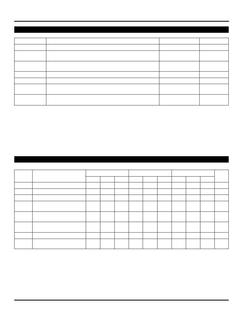
PIN CONFIGURATION/BLOCK DIAGRAM
D
SET
RESET
CLK
Q
L
L
L
Z
L
H
L
L
Z
H
X
H
L
X
H
X
L
H
X
L
X
H
H
X
UNDEF
Note 1.
Z = LOW-to-HIGH transition.
1
2345
6
7
8
9
10
VCC
D
/
D
C
LK
/CLK
SET
Q
/
Q
RESET
VEE
D
Flip-Flop
SR
MSOP
TOP VIEW
Pin
Function
D, /D
Data Input (ECL)
CLK, /CLK
Clock Input (ECL)
Q, /Q
Data Output (ECL)
V
CC
, V
EE
Power Supply
SET
ECL Asynchonous Set
RESET
ECL Asynchonous Reset
Rev.: C
Amendment: /0
Issue Date:
March 2003
ECL ProTM
SY10EP53V
FINAL
TRUTH TABLE
(1)
PIN NAMES
ECL ProTM
ECL Pro is a trademark of Micrel, Inc.
2
ECL ProTM
SY10EP53V
Micrel
Symbol
Rating
Value
Unit
V
CC
-- V
EE
Power Supply Voltage
6V
V
V
IN
Input Voltage (V
CC
= 0V, V
IN
not more negative than V
EE
)
≠6.0 to 0
V
Input Voltage (V
EE
= 0V, V
IN
not more positive than V
CC
)
+6.0 to 0
V
I
OUT
Output Current
≠Continuous
50
mA
≠Surge
100
T
A
Operating Temperature Range
≠40 to +85
∞
C
T
store
Storage Temperature Range
≠65 to +150
∞
C
JA
Package Thermal Resistance
≠Still-Air
113
∞
C/W
≠500lfpm
96
JC
Package Thermal Resistance
42
∞
C/W
(Junction-to-Case)
Note 1.
Permanent device damage may occur if ABSOLUTE MAXIMUM RATINGS are exceeded. This is a stress rating only and functional operation
is not implied at conditions other than those detailed in the operational sections of this data sheet. Exposure to ABSOLUTE MAXIMUM
RATlNG conditions for extended periods may affect device reliability.
ABSOLUTE MAXIMUM RATINGS
(1)
T
A
= ≠40
∞
C
T
A
= +25
∞
C
T
A
= +85
∞
C
Symbol
Parameter
Min.
Typ.
Max.
Min.
Typ.
Max.
Min.
Typ.
Max.
Unit
I
EE
Power Supply Current
--
--
47
--
35
47
--
--
47
mA
V
OH
Output HIGH Voltage
(3)
3865
3990
4115
3930
4055
4180
3990
4115
4240
mV
V
OL
Outuput LOW Voltage
(3)
3050
3190
3315
3050
3255
3380
3050
3315
3440
mV
V
IH
Input HIGH Voltage
3790
--
4115
3855
--
4180
3915
--
4240
mV
(Single-Ended)
V
IL
Input LOW Voltage
3065
--
3390
3130
--
3455
3190
--
3515
mV
(Single-Ended)
V
IHCMR
Input HIGH Voltage
(4)
2.0
--
V
CC
2.0
--
V
CC
2.0
--
V
CC
V
Common Mode Range (Diff.)
I
IH
Input HIGH Current
--
--
150
--
--
150
--
--
150
µ
A
I
IL
Input LOW Current
D
0.5
--
--
0.5
--
--
0.5
--
--
µ
A
/D
≠150
--
--
≠150
--
--
≠150
--
--
Note 1.
10EP circuits are designed to meet the DC specifications shown in the above table after thermal equilibrium has been established. The circuit
is in a test socket or mounted on a printed circuit board and traverse airflow greater than 500lfpm is maintained.
Note 2.
Input and output parameters vary 1:1 with V
CC
. V
CC
can vary ≠0.5V to +0.5V.
Note 3.
All loading with 50
to V
CC
≠2.0V.
Note 4.
V
IHCMR
(min) varies 1:1 with V
EE
, V
IHCMR
(max) varies 1:1 with V
CC
. The V
IHCMR
range is referenced to the most positive side of the differen-
tial input signal.
PECL DC ELECTRICAL CHARACTERISTICS
(1)
V
CC
= 5.0V, V
EE
= 0V
(2)

3
ECL ProTM
SY10EP53V
Micrel
T
A
= ≠40
∞
C
T
A
= +25
∞
C
T
A
= +85
∞
C
Symbol
Parameter
Min.
Typ.
Max.
Min.
Typ.
Max.
Min.
Typ.
Max.
Unit
I
EE
Power Supply Current
--
--
47
--
35
47
--
--
47
mA
V
OH
Output HIGH Voltage
(3)
2165
2290
2415
2230
2355
2480
2290
2415
2540
mV
V
OL
Outuput LOW Voltage
(3)
1350
1490
1615
1350
1555
1680
1350
1615
1740
mV
V
IH
Input HIGH Voltage
2090
--
2415
2155
--
2480
2215
--
2540
mV
(Single-Ended)
V
IL
Input LOW Voltage
1365
--
1690
1430
--
1755
1490
--
1815
mV
(Single-Ended)
V
IHCMR
Input HIGH Voltage
(4)
2.0
--
V
CC
2.0
--
V
CC
2.0
--
V
CC
V
Common Mode Range (Diff.)
I
IH
Input HIGH Current
--
--
150
--
--
150
--
--
150
µ
A
I
IL
Input LOW Current
D
0.5
--
--
0.5
--
--
0.5
--
--
µ
A
/D
≠150
--
--
≠150
--
--
≠150
--
--
Note 1.
10EP circuits are designed to meet the DC specifications shown in the above table after thermal equilibrium has been established. The circuit
is in a test socket or mounted on a printed circuit board and traverse airflow greater than 500lfpm is maintained.
Note 2.
Input and output parameters vary 1:1 with V
CC
. V
CC
can vary ≠0.3V to +0.5V.
Note 3.
All loading with 50
to V
CC
≠2.0V.
Note 4.
V
IHCMR
(min) varies 1:1 with V
EE
, V
IHCMR
(max) varies 1:1 with V
CC
. The V
IHCMR
range is referenced to the most positive side of the differential
input signal.
LVPECL DC ELECTRICAL CHARACTERISTICS
(1)
V
CC
= 3.3V, V
EE
= 0V
(2)
T
A
= ≠40
∞
C
T
A
= +25
∞
C
T
A
= +85
∞
C
Symbol
Parameter
Min.
Typ.
Max.
Min.
Typ.
Max.
Min.
Typ.
Max.
Unit
I
EE
Power Supply Current
(3)
--
--
47
--
35
47
--
--
47
mA
V
OH
Output HIGH Voltage
(4)
≠1135
≠0885
≠1070
≠0945
≠0820
≠1010
≠0760
mV
V
OL
Outuput LOW Voltage
(4)
≠1950
≠1685
≠1950
≠1745
≠1620
≠1950
≠1560
mV
V
IH
Input HIGH Voltage
≠1210
≠0885
≠1145
--
≠0820
≠1085
--
≠0760
mV
V
IL
Input LOW Voltage
≠1935
≠1610
≠1870
--
≠1545
≠1810
--
≠1485
mV
V
IHCMR
Input HIGH Voltage
V
EE
+2.0
V
CC
V
EE
+2.0
V
CC
V
EE
+2.0
V
CC
V
Common Mode Range
(5)
I
IH
Input HIGH Current
--
--
150
--
--
150
--
--
150
µ
A
I
IL
Input LOW Current
0.5
--
--
0.5
--
--
0.5
--
--
µ
A
Note 1.
10EP circuits are designed to meet the DC specifications shown in the above table after thermal equilibrium has been established. The circuit
is in a test socket or mounted on a printed circuit board and traverse airflow greater than 500lfpm is maintained.
Note 2.
Input and output parameters vary 1:1 with V
CC
.
Note 3.
V
CC
= 0V, V
EE
= V
EE
(min) to V
EE
(max), all other pins floating.
Note 4.
All loading with 50
to V
CC
≠ 2.0V.
Note 5.
V
IHCMR
min varies 1:1 with V
EE
, max varies 1:1 with V
CC
.
ECL/LVECL DC ELECTRICAL CHARACTERISTICS
(1)
V
CC
= 0V, V
EE
= ≠5.5V to ≠3.0V
(2)
4
ECL ProTM
SY10EP53V
Micrel
T
A
= ≠40
∞
C
T
A
= +25
∞
C
T
A
= +85
∞
C
Symbol
Parameter
Min.
Typ.
Max.
Min.
Typ.
Max.
Min.
Typ.
Max.
Unit
f
MAX
Maximum Toggle Frequency
(1)
--
3.0
--
--
3.0
--
--
3.0
--
GHz
t
PLH
Propagation Delay to Output
ps
t
PHL
Differential
CLK
Q, /Q
175
--
325
200
275
350
250
--
400
SET, RESET
Q, /Q
200
--
360
250
330
420
325
--
475
t
RR
Reset Recovery Time
225
--
--
200
140
--
185
--
--
ps
t
S
Setup Time
150
50
--
150
50
--
150
50
--
ps
t
H
Hold Time
150
50
--
150
50
--
150
50
--
ps
t
PW
Minimum Pulse Width
550
450
--
550
450
--
550
450
--
ps
V
PP
Input Voltage Swing
--
--
--
--
TBD
--
--
--
--
mV
(Differential)
t
r
Output Rise/Fall Times
Q
50
--
180
60
130
200
70
--
220
ps
t
f
(20% to 80%)
Note 1.
f
MAX
guaranteed for functionality only. V
OL
and V
OH
levels are guaranteed at DC only.
AC ELECTRICAL CHARACTERISTICS
V
CC
= 0V, V
EE
= ≠5.5V to ≠3.0V; V
CC
= 3.0V to 5.5V, V
EE
= 0V
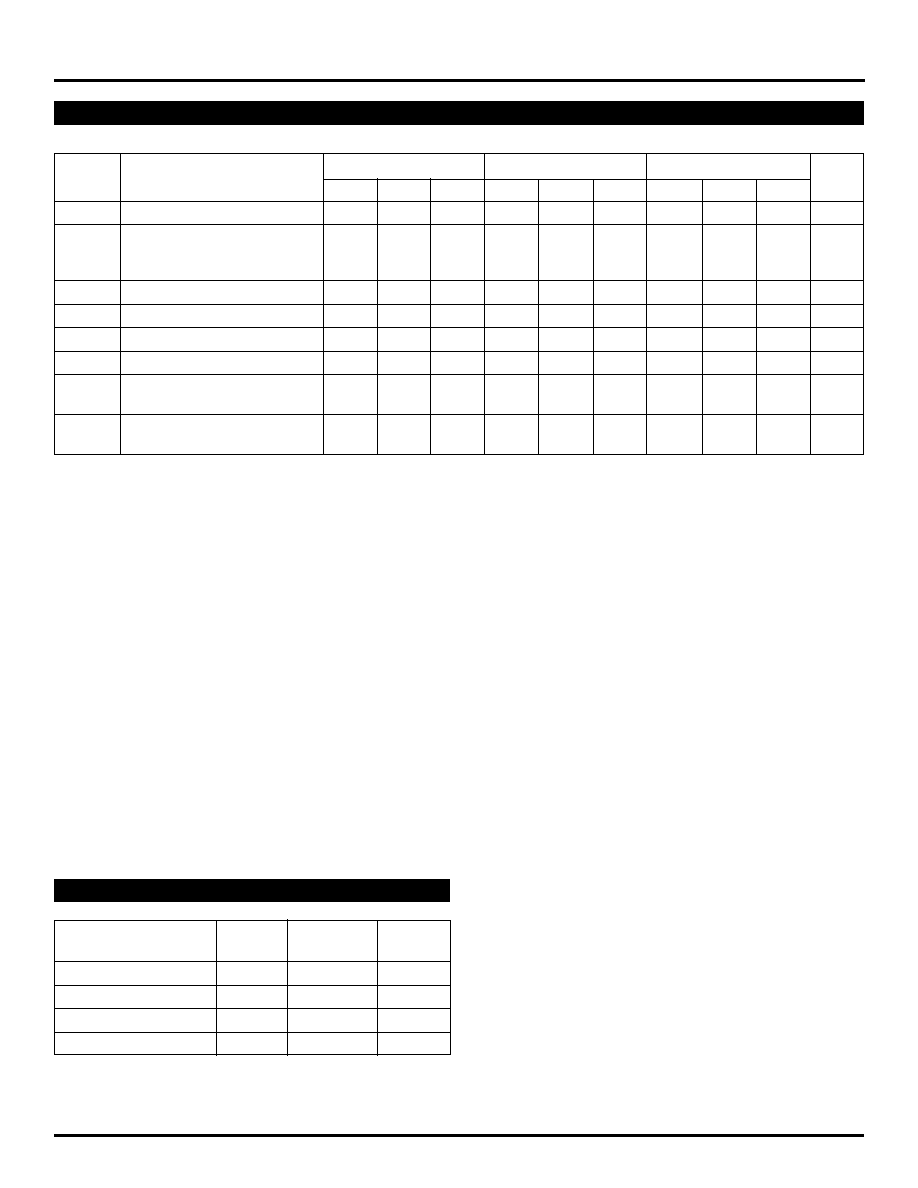
PRODUCT ORDERING CODE
Ordering
Package
Operating
Package
Code
Type
Range
Marking
SY10EP53ZC
K10-1
Commercial
HEP53V
SY10EP53ZCTR
(1)
K10-1
Commercial
HEP53V
SY10EP53ZI
(2)
K10-1
Industrial
HEP53V
SY10EP53ZITR
(1,2)
K10-1
Industrial
HEP53V
Note 1.
Tape and Reel.
Note 2.
Recommended for new designs.
5
ECL ProTM
SY10EP53V
Micrel
Rev. 00
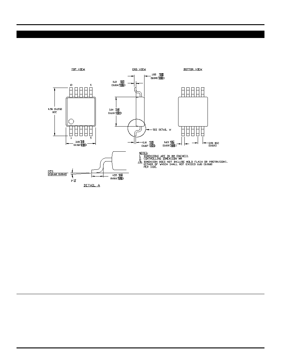
10 LEAD MSOP (K10-1)
MICREL, INC.
1849 FORTUNE DRIVE
SAN JOSE, CA 95131
USA
TEL
+ 1 (408) 944-0800
FAX
+ 1 (408) 944-0970
WEB
http://www.micrel.com
The information furnished by Micrel in this datasheet is believed to be accurate and reliable. However, no responsibility is assumed by Micrel for its use.
Micrel reserves the right to change circuitry and specifications at any time without notification to the customer.
Micrel Products are not designed or authorized for use as components in life support appliances, devices or systems where malfunction of a product can
reasonably be expected to result in personal injury. Life support devices or systems are devices or systems that (a) are intended for surgical implant into
the body or (b) support or sustain life, and whose failure to perform can be reasonably expected to result in a significant injury to the user. A Purchaser's
use or sale of Micrel Products for use in life support appliances, devices or systems is at Purchaser's own risk and Purchaser agrees to fully indemnify
Micrel for any damages resulting from such use or sale.
© 2003 Micrel, Incorporated.