 | –≠–ª–µ–∫—Ç—Ä–æ–Ω–Ω—ã–π –∫–æ–º–ø–æ–Ω–µ–Ω—Ç: SY10H352 | –°–∫–∞—á–∞—Ç—å:  PDF PDF  ZIP ZIP |
DESCRIPTION
s
Single 5V power supply
s
All V
CC
pins isolated on chip
s
Differentially drive balanced lines
s
t
pd
1.3ns typical
s
Fully compatible with ON Semiconductor MC10H352
s
Available in 20-pin PLCC package
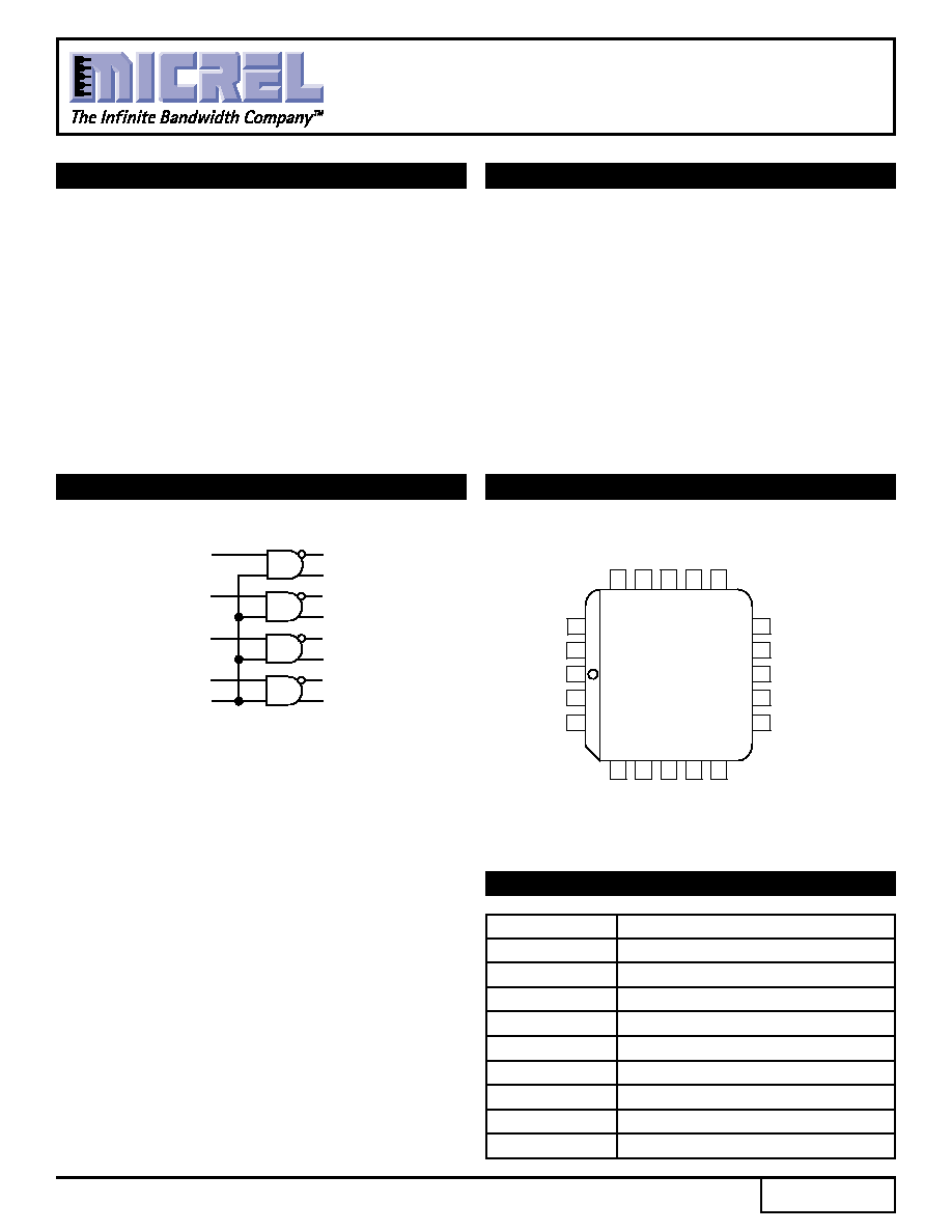
The SY10H352 is a quad translator for interfacing data
between a CMOS logic section and the PECL section of
digital systems when only a +5.0V VDC power supply is
available. The SY10H352 has CMOS compatible inputs
and PECL complementary open-emitter outputs that allow
use as an inverting/non-inverting translator or as a
differential line driver. When the common strobe input is
at a low logic level, it forces all true outputs to the PECL
low logic state (
+3.2V) and all inverting outputs to the
PECL high logic state (
+4.1V).
The SY10H352 can also be used with the SY10H350
to transmit and receive CMOS information differentially
via balanced twisted pair lines.
FEATURES
QUAD CMOS-to-PECL
TRANSLATOR
BLOCK DIAGRAM
SY10H352
FINAL
1
Rev.: A
Amendment: /1
Issue Date:
August 2000
PIN CONFIGURATION
1
20
19
18
17
16
15 14
13
12
11
10
9
8
7
6
5
4
3
2
NC
D3
VCCT
GND
Common Strobe
/Q2
VCCE
/Q1
Q1
NC
D0
D1
VCC1
/Q0
Q0
D2
VCC2
/Q3
Q3
Q2
Top View
PLCC
J20-1
1
2
5
4
14
12
8
7
9
16
17
19
18
D1
D0
D3
D2
/Q1
Q1
/Q0
Q0
/Q3
Q3
/Q2
Q2
COMMON
STROBE
V
CC
(+5 V
DC
) = Pins 6, 11, 15, 20;
GND = Pin 10
Pin
Function
D0 ≠ D3
Inputs
Q0 ≠ Q3
Outputs
/Q0 ≠ /Q3
Inverted outputs
VCC1
PECL V
CC
(5.0V)
VCCE
PECL V
CC
(5.0V)
VCCT
CMOS V
CC
(5.0V)
VCC2
PECL V
CC
(5.0V)
Common Strobe
Common Strobe
GND
Ground
PIN NAMES

2
SY10H352
Micrel
Symbol
Parameter
Value
Unit
V
CC
Power Supply Voltage
≠0.5 to +7.0
V
I
O
Output Current
≠Continuous
50
mA
≠Surge
100
T
store
Storage Temperature
≠65 to +150
∞
C
T
A
Operating Temperature
0 to +85
∞
C
NOTE:
1. Permanent device damage may occur if ABSOLUTE MAXIMUM RATINGS
are exceeded. This is a stress rating only and functional operation is not
implied at conditions other than those detailed in the operational sections
of this data sheet. Exposure to ABSOLUTE MAXIMUM RATlNG conditions
for extended periods may affect device reliability.
ABSOLUTE MAXIMUM RATINGS
(1)
TRUTH TABLE
CS
D
Q
/Q
H
L
L
H
H
H
H
L
H
Open
H
L
L
X
L
H
Open
L
L
H
Open
H
H
L
Open
Open
H
L
T
A
= 0
∞
C
T
A
= +25
∞
C
T
A
= +85
∞
C
Symbol
Parameter
Min.
Max.
Min.
Typ.
Max.
Min.
Max.
Unit
Condition
I
CC
Power Supply Current ECL
(1)
--
45
--
--
45
--
45
mA
No output
TTL
(2)
--
15
--
--
15
--
15
loads
I
R
Reverse Current
--
20
--
--
20
--
20
µ
A
(Pins 7, 8, 12, 14)
I
INH
Reverse Current, (Pin 9)
--
80
--
--
80
--
80
µ
A
I
F
Forward Current
--
≠0.6
--
--
≠0.6
--
≠0.6
mA
(Pins 7, 8, 12, 14)
I
INL
Forward Current, (Pin 9)
--
≠2.4
--
--
≠2.4
--
≠2.4
mA
V
BR(in)
Input Breakdown Voltage
5.5
--
5.5
--
--
5.5
--
V
V
I
Input Clamp Voltage
--
≠1.5
--
--
≠1.5
--
≠1.5
V
I
IN
= ≠18mA
V
OH
Output HIGH Voltage
(3)
3.98
4.16
4.02
--
4.19
4.09
4.28
V
V
OL
Output LOW Voltage
(3)
3.05
3.37
3.05
--
3.37
3.05
3.37
V
V
IH
Input HIGH Voltage
3.15
--
3.15
--
--
3.15
--
V
V
IL
Input LOW Voltage
--
1.5
--
--
1.5
--
1.5
V
DC ELECTRICAL CHARACTERISTICS
VCC1 = VCC2 = VCCE = VCCT = 4.75V to 5.25V
NOTES:
1. Total ICC at VCC1, VCC2 and VCCE.
2. ICC at ICCT.
3. These values are for VCC = 5.0V. Level Specifications will vary 1:1 VCC.
3
SY10H352
Micrel
PRODUCT ORDERING CODE
Ordering
Package
Operating
V
CC
Range
Code
Type
Range
(V)
SY10H352JC
J20-1
Commercial
+4.75 to +5.25
SY10H352JCTR
J20-1
Commercial
+4.75 to +5.25
NOTES:
1. Propagation delay is measured on this circuit from V
CC2
on the input waveform to the 50% point on the output waveform.
2. These parameters are guaranteed but not tested.
T
A
= 0
∞
C
T
A
= +25
∞
C
T
A
= +85
∞
C
Symbol
Parameter
Min.
Max.
Min.
Typ.
Max.
Min.
Max.
Unit
Condition
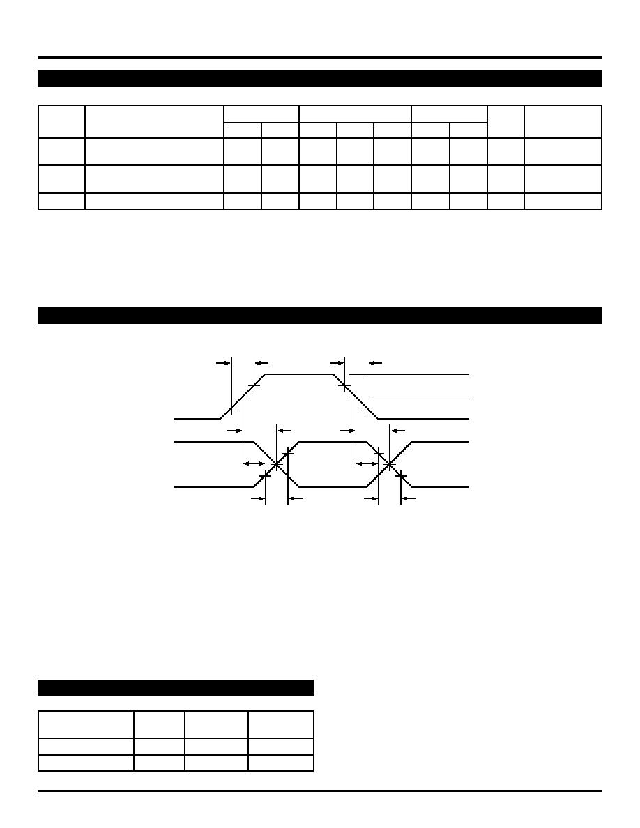
t
PLH
Propagation Delay
(1)
0.4
1.9
0.4
--
2.0
0.4
2.1
ns
50
to VCC≠2V
t
PHL
t
r
Output Rise/Fall Time
0.4
1.9
0.4
--
2.0
0.4
2.1
ns
50
to VCC≠2V
t
f
(20% to 80%)
f
MAX
Maximum Input Frequency
(2)
150
--
150
--
--
150
--
MHz
50
to VCC≠2V
AC ELECTRICAL CHARACTERISTICS
VCC1 = VCC2 = VCCE = VCCT = 4.75V to 5.25V
SWITCHING WAVEFORM
COMPLEMENT
INPUT
50%
1ns/V (typical)
V
CC
10%
90%
V
CC
/2
0V
t
THL
TRUE
20%
80%
50%
t
TLH
1ns/V (typical)
t
PLH
t
PHL
t
PLH
t
PHL
Figure 1. Propagation Delay and Transition Times

4
SY10H352
Micrel
20 LEAD PLASTIC LEADED CHIP CARRIER (J20-1)
MICREL-SYNERGY
3250 SCOTT BOULEVARD
SANTA CLARA
CA 95054
USA
TEL
+ 1 (408) 980-9191
FAX
+ 1 (408) 914-7878
WEB
http://www.micrel.com
This information is believed to be accurate and reliable, however no responsibility is assumed by Micrel for its use nor for any infringement of patents or
other rights of third parties resulting from its use. No license is granted by implication or otherwise under any patent or patent right of Micrel Inc.
© 2000 Micrel Incorporated
Rev. 00