DESCRIPTION
s
2.5GHz min F
MAX
s
2.3V to 5.7V power supply
s
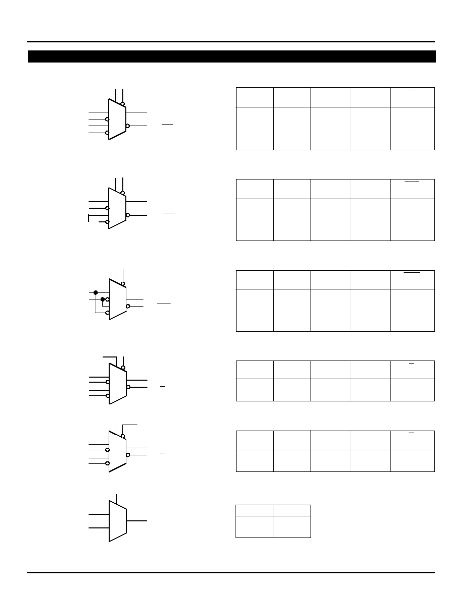
Provides for any logic function of 2 variables
s
Provides for 2-input muxing
s
Fully differential
s
Source terminated CML outputs for fast edge rates
s
Accepts LVDS, PECL, PECL, CML, TTL, LVPECL,
input logic levels
s
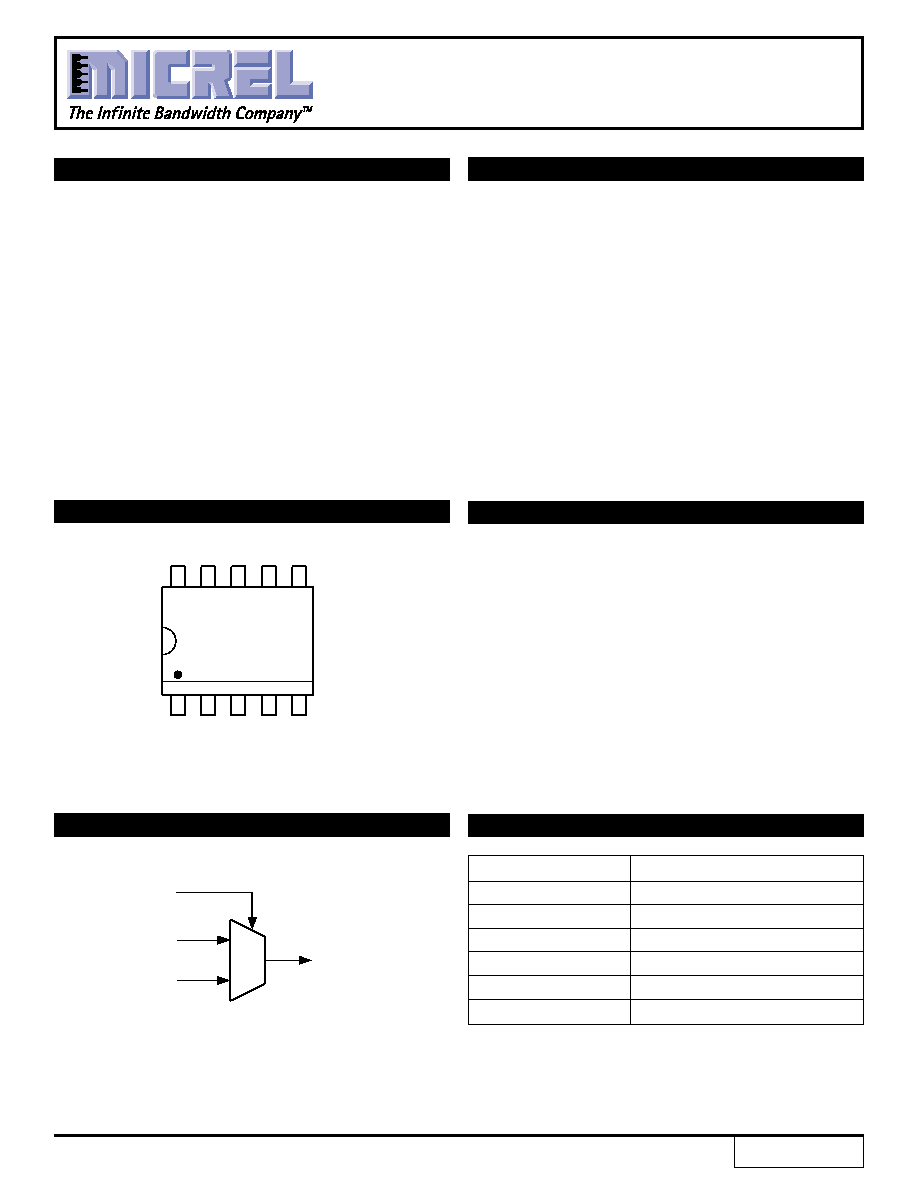
Available in a tiny 10-pin MSOP
The SY55851U is a highly flexible, universal logic gate
capable of upto 2.5GHz operation. It's differential inputs
and outputs will produce any of 9 possible logic functions
of two Boolean variables. It can be configured as any of
the following gates: AND, NAND, OR, NOR, XOR, XNOR,
DELAY, NEGATION (NOT). Also, the SY55851U can
function as a 2-input multiplexer.
SY55851U inputs can be terminated with a single
resistor between the true and the complement pins of a
given input.
The SY55851U is a member of Micrel's new Super-
LiteTM family of high-speed logic devices. This family
features very small packaging, high signal integrity, and
operation at many different supply voltages.
FEATURES
AnyGateTM
CML LOGIC CHIP
SuperLiteTM
SY55851U
APPLICATIONS
s
Port bypass
s
Data communication systems
s
Wireless communication systems
s
Telecom systems
PIN CONFIGURATION
FUNCTIONAL BLOCK DIAGRAM
1
Rev.: B
Amendment: /0
Issue Date:
August 2000
S
0
1
A
B
S
Q
PIN NAMES
Pin
Function
A, /A
Input Data
B, /B
Input Data
Q, /Q
Output Data
S, /S
Input Selector
GND
Ground
V
CC
V
CC
S
/S
A
/A GND
VCC /B
B
Q
/Q
7
6
4
5
1
10
9
8
2
3
851U
AnyGateTM and SuperLiteTM are trademarks of Micrel, Inc.
2
SuperLiteTM
SY55851U
Micrel
PIN DESCRIPTIONS
A, /A � CML Input (Differential)
This is one of the inputs to the logic block. For a 2-
variable logic function, it is either a constant value or a
Boolean input. For a 2-input mux, this signal represents
the output when S is set to logic zero.
B, /B � CML Input (Differential)
This is one of the inputs to the logic block. For a 2-
variable logic function, it is either a constant value or a
Boolean input. For a 2-input mux, this signal represents
the output when S is set to logic one.
Q, /Q � CML Output (Differential)
This is the output of the logic block.
S, /S � CML Input (Differential)
This is one of the inputs to the logic block. It represents
either one Boolean input for a 2-variable logic function,
or the select input for a 2-input mux.
FUNCTIONAL DESCRIPTION
V
CC
NC
X
/X
Figure 1. Hard Wiring A Logic "1"
(1)
NC
V
CC
> 3.0V
NC
X
/X
NC
V
CC
3.0V
VCC
X
/X
Figure 2. Hard Wiring A Logic "0"
(1)
Establishing Static Logic Inputs
The true pin of an input pair is internally biased to ground
through a 75k
resistor. The complement pin of an input
pair is internally biased halfway between V
CC
and ground
by a voltage divider consisting of two 75k
resistors. To
keep an input at static logic zero at V
CC
> 3.0V, leave both
inputs unconnected. For V
CC
3.0V, connect the
complement input to V
CC
and leave the true input
unconnected. To make an input static logic one, connect
the true input to V
CC
, leave the complement input
unconnected. These are the only two safe ways to cause
inputs to be at a static value. In particular, no input pin
should be directly connected to ground. All NC (no connect)
pins should be unconnected.
NOTE:
1. X is either A, B, S input. /X is either /A, /B, /S input.
3
SuperLiteTM
SY55851U
Micrel
( )
A
B
S
Q
/Q
L
H
L
L
H
L
H
H
H
L
H
L
L
H
L
H
L
H
L
H
+
(
+
)
A
B
S
Q
/Q
L
H
L
L
H
H
H
L
H
L
L
H
H
H
L
H
H
H
H
L
A
B
S
Q
/Q
L
X
L
L
H
H
X
L
H
L
TRUTH TABLES
AND/NAND
Q
/Q
S
/S
A
/A
B
/B
NC
(
)
NC
OR/NOR
Q
/Q
S
/S
A
/A
B
/B
+
(
+ )
V
CC
NC
XOR/XNOR
Q
/Q
S
/S
A
/A
B
/B
(
)
DELAY/NEGATION
Q
/Q
S
A
/B
/S
B
/A
NC
NC
A
B
S
Q
/Q
X
L
H
L
H
X
H
H
H
L
Q
/Q
S
A
/B
/S
B
/A
V
CC
NC
()
A
B
S
Q
/Q
L
L
L
L
H
L
H
L
L
H
L
L
H
L
H
L
H
H
H
L
Q
S
A
B
0
1
S
Q
H
B
L
A
2:1 MUX
4
SuperLiteTM
SY55851U
Micrel
Symbol
Rating
Value
Unit
V
CC
Power Supply Voltage
�0.5 to +6.0
V
V
I
Input Voltage
�0.5 to V
CC
+0.5
V
V
O
CML Output Voltage
V
CC
�1.0 to V
CC
+0.5
V
T
A
Operating Temperature Range
�40 to +85
�
C
T
store
Storage Temperature Range
�65 to +150
�
C
ABSOLUTE MAXIMUM RATINGS
(1)
NOTE:
1. Permanent device damage may occur if ABSOLUTE MAXIMUM RATINGS are exceeded. This is a stress rating only and functional operation is not implied
at conditions other than those detailed in the operational sections of this data sheet. Exposure to ABSOLUTE MAXIMUM RATlNG conditions for extended
periods may affect device reliability.
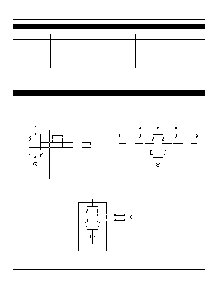
CML TERMINATION
100
100
100
100
SY55851U
v
cc
v
cc
100
50
50
8mA
Figure 3a.
Differentially Terminated
(50
Load CML Output)
100
100
100
50
SY55851U
v
cc
50
8mA
50
100
50
Figure 3b.
Individually Terminated
(50
Load CML Output)
All inputs accept the output from any other member of
this family. All outputs are source terminated 100
CML
differential drivers as shown in Figures 3 and 4. SY55851U
expects the inputs to be terminated, and that good high
speed design practices be adhered to. SY55851U inputs
are designed to accept a termination resistor between the
true and complement inputs of a differential pair. 0402 form
factor chip resistors will fit with some trace fanout.
100
100
200
SY55851U
V
CC
8mA
100
100
Figure 4.
100
Load CML Output
5
SuperLiteTM
SY55851U
Micrel
Symbol
Parameter
Min.
Typ.
Max.
Unit
Condition
V
ID
Differential Input Voltage
100
--
--
mV
V
IH
Input HIGH Voltage
1.6
--
V
CC
V
V
IL
Input LOW Voltage
1.5
--
V
CC
� 0.1
V
V
OH
Output HIGH Voltage
V
CC
� 0.020
V
CC
� 0.010
V
CC
V
No Load
V
OL
Output LOW Voltage
V
CC
� 0.97
V
CC
� 0.825
V
CC
� 0.700
V
No Load
V
OS
Output Voltage Swing
(2)
0.700
0.800
0.950
V
No Load
0.400
100
Environment
(4)
0.200
50
Environmnet
(3)
R
DRIVE
Output Source Impedance
80
100
120
CML DC ELECTRICAL CHARACTERISTICS
V
CC
= 2.3V to 5.7V; GND = 0V; T
A
= �40
�
C to +85
�
C
(1)
NOTES:
1. Equilibrium temperature.
2. Actual voltage levels and differential swing will depend on customer termination scheme. Typically, a 400mV swing is available in the 100
environment
and a 200mV swing in the 50
environment. Refer to the "CML Termination" diagram for more details.
3. See Figure 3a and 3b.
4. See Figure 4.
Symbol
Parameter
Min.
Typ.
Max.
Unit
Condition
(1)
f
MAX
Max. Operating Frequency
2.5
--
--
GHz
t
PIN0
Propagation Delay,
--
--
350
ps
S to Q
t
PIN1
Propagation Delay,
--
--
350
ps
A to Q
t
PIN2
Propagation Delay,
--
--
350
ps
B to Q
t
r
CML Output Rise/Fall Times
TBD
--
110
ps
t
f
(20% to 80%)
AC ELECTRICAL CHARACTERISTICS
V
CC
= 2.3V to 5.7V; GND = 0V; T
A
= �40
�
C to +85
�
C
T
A
= �40
�
C
T
A
= 0
�
C
T
A
= +25
�
C
T
A
= +85
�
C
Symbol
Parameter
Min.
Max.
Min.
Max.
Min.
Max.
Min.
Max.
Unit
V
CC
Power Supply Voltage
2.3
5.7
2.3
5.7
2.3
5.7
2.3
5.7
mA
I
CC
Power Supply Current
--
40
--
40
--
40
--
40
mA
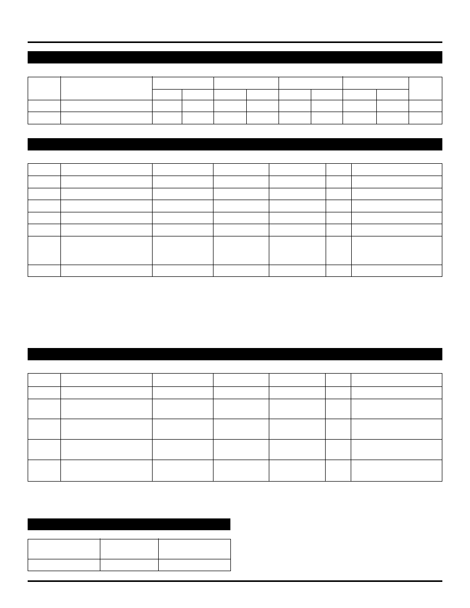
DC ELECTRICAL CHARACTERISTICS
V
CC
= 2.3V to 5.7V; GND = 0V
PRODUCT ORDERING CODE
Ordering
Package
Operating
Code
Type
Range
SY55851UKC
K10-1
Commercial
NOTE:
1. Tested using environment of Figure 3b, 50
load CML output.