1
SuperLiteTM
SY55852U
Micrel
DESCRIPTION
s
2.5GHz min. f
MAX
s
2.3V to 5.7V power supply
s
Single bit register memory
s
Synchronizes 1 bit of data to a clock
s
Optimized to work with SuperLiteTM family
s
Fully differential
s
Accepts CML, PECL, LVPECL input logic levels
s
Source terminated CML outputs for fast edge rates
s
Available in a tiny 10-pin MSOP
The SY55852U is a flip-flop used to synchronize data
to a clock. Its differential output will reproduce and
remember the value on its input at the rising edge of the
clock. In addition, an asynchronous, level sensitive reset
is provided. For a synchonous reset, the SY55851U
AnyGateTM can be used.
SY55852U inputs can be terminated with a single
resistor between the true and complement pins of a given
input.
The SY55852U is a member of Micrel's SuperLiteTM
family of high-speed CML logic. This family features very
small packaging and 2.3V to 5.7V operation.
FEATURES
D FLIP-FLOP
SuperLiteTM
SY55852U
FINAL
APPLICATIONS
s
High-speed logic
s
OC-48 communication systems
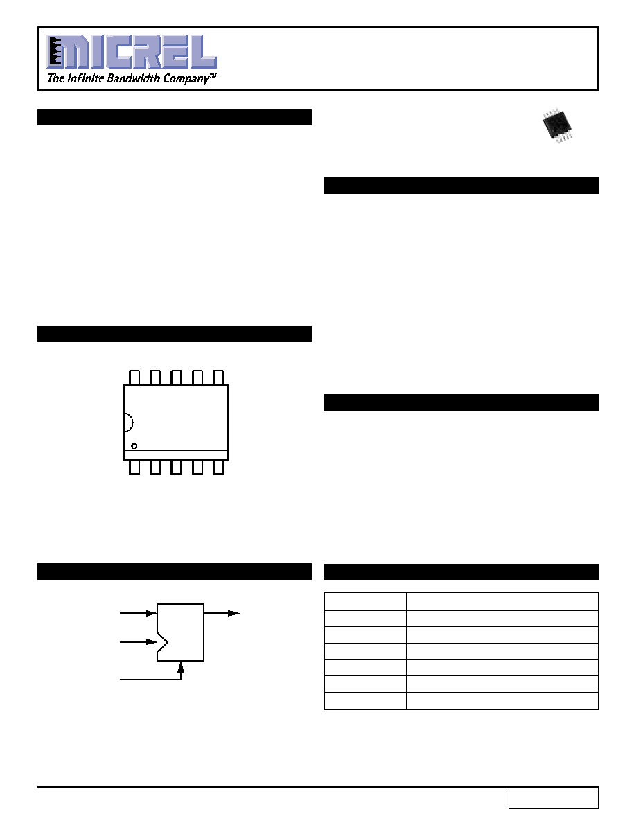
PIN CONFIGURATION
FUNCTIONAL BLOCK DIAGRAM
Rev.: B
Amendment: /0
Issue Date:
March 2003
PIN NAMES
Pin
Function
D, /D
CML/PECL/LVPECL Data Input
CLK, /CLK
CML/PECL/LVPECL Clock Input
R, /R
CML/PECL/LVPECL Reset Input
Q, /Q
CML Data Output
GND
Ground
V
CC
V
CC
D
/D CLK /CLK GND
VCC /R
R
Q
/Q
7
6
4
5
1
10
9
8
2
3
Top View
MSOP
SuperLite is a trademark of Micrel, Inc.
D
Q
R
CLOCK
RESET
DATA
OUT
SuperLiteTM
2
SuperLiteTM
SY55852U
Micrel
PIN DESCRIPTIONS
D, /D � CML/PECL/LVPECL Input (Differential)
This is the single bit of data that gets clocked in and
remembered.
CLK, /CLK � CML/PECL/LVPECL Input (Differential)
The rising edge of this signal is the clock signal that
determines when the Boolean value at the data input
gets stored.
R, /R � CML/PECL/LVPECL Input (Differential)
This is an asynchronous active high level reset, that
forces the flip-flop into a known state, namely zero.
Q, /Q � CML Output (Differential)
This is the output of the flip-flop.
FUNCTIONAL DESCRIPTION
V
CC
NC
X
/X
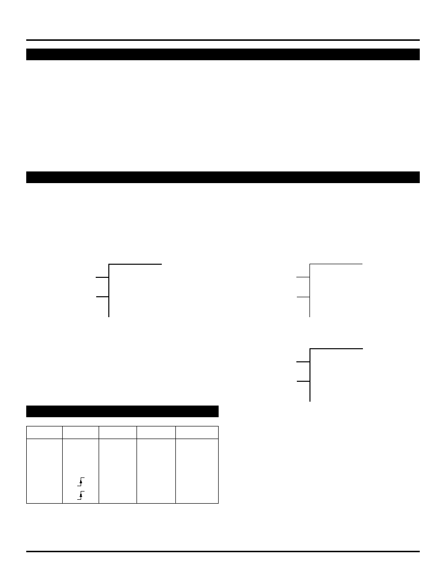
Figure 1. Hard Wiring a Logic "1"
(1)
NC
V
CC
> 3.0V
NC
X
/X
NC
V
CC
3.0V
X
/X
V
CC
Figure 2. Hard Wiring a Logic "0"
(1)
Establishing Static Logic Inputs
The true pin of an input pair is internally biased to ground
through a 75k
resistor. The complement pin of an input
pair is internally biased halfway between V
CC
and ground
by a voltage divider consisting of two 75k
resistors. To
keep an input at static logic zero at V
CC
> 3.0V, leave both
inputs unconnected. For V
CC
3.0V, connect the
complement inputs to V
CC
and leave the true inputs
unconnected. To make an input static logic one, connect
the true input to V
CC
, leave the complement input
unconnected. These are the only safe ways to cause inputs
to be at a static value. In particular, no input pin should be
directly connected to ground. All NC (no connect) pins
should be unconnected.
Note 1.
X is either D, CLK, R input. /X is either /D, /CLK, /R input.
D
CLK
R
Q
/Q
X
X
1
0
1
X
0
0
Q
N-1
/Q
N-1
X
1
0
Q
N-1
/Q
N-1
0
0
0
1
1
0
1
0
TRUTH TABLE
3
SuperLiteTM
SY55852U
Micrel
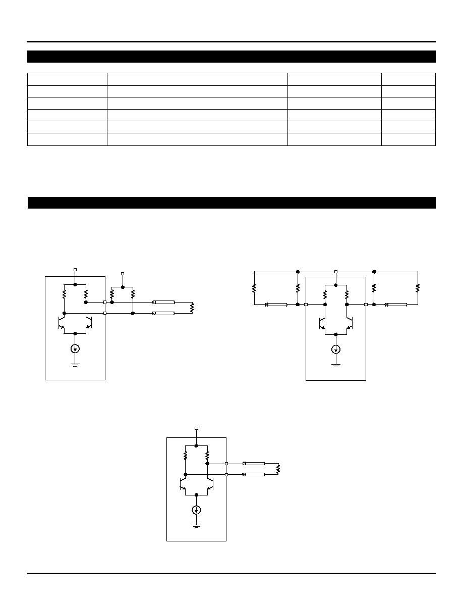
CML TERMINATION
100
100
100
100
SY55852U
v
cc
v
cc
100
50
50
8mA
Figure 3a.
Differentially Terminated
(50
Load CML Output)
All inputs accept the output from any other member of
this family. All outputs are source terminated 100
CML
differential drivers as shown in Figures 3 and 4. SY55852U
expects the inputs to be terminated, and that good high
speed design practices be adhered to. SY55852U inputs
are designed to accept a termination resistor between the
true and complement inputs of a differential pair. 0402 form
factor chip resistors will fit with some trace fanout.
100
100
100
50
SY55852U
v
cc
50
8mA
50
100
50
Figure 3b.
Individually Terminated
(50
Load CML Output)
100
100
200
SY55852U
V
CC
8mA
100
100
Figure 4.
100
Load CML Output
Symbol
Rating
Value
Unit
V
CC
Power Supply Voltage
�0.5 to +6.0
V
V
IN
Input Voltage
�0.5 to V
CC
+0.5
V
V
OUT
CML Output Voltage
V
CC
�1.0 to V
CC
+0.5
V
T
A
Operating Temperature Range
�40 to +85
�
C
T
store
Storage Temperature Range
�65 to +150
�
C
ABSOLUTE MAXIMUM RATINGS
(1)
Note 1.
Permanent device damage may occur if ABSOLUTE MAXIMUM RATINGS are exceeded. This is a stress rating only and functional operation
is not implied at conditions other than those detailed in the operational sections of this data sheet. Exposure to ABSOLUTE MAXIMUM
RATlNG conditions for extended periods may affect device reliability.
4
SuperLiteTM
SY55852U
Micrel
T
A
= �40
�
C
T
A
= 0
�
C
T
A
= +25
�
C
T
A
= +85
�
C
Symbol
Parameter
Min.
Max.
Min.
Max.
Min.
Max.
Min.
Max.
Unit
V
CC
Power Supply Voltage
2.3
5.7
2.3
5.7
2.3
5.7
2.3
5.7
V
I
CC
Power Supply Current
--
36
--
36
--
36
--
36
mA
Note 1.
Specification for packaged product only.
DC ELECTRICAL CHARACTERISTICS
(1)
V
CC
= 2.3V to 5.7V; GND = 0V
Symbol
Parameter
Min.
Typ.
Max.
Unit
Condition
(2)
f
MAX
Max. Operating Frequency
2.5
--
--
GHz
t
PLH
Propagation Delay,
CLK to Q
--
--
400
ps
t
PHL
R to Q
--
--
500
t
S
Set-Up Time
40
--
--
ps
t
H
Hold Time
40
--
--
ps
t
RR
Reset Recovery
400
--
--
ps
t
PW
Minimum Pulse Width
CLK to Q
V
CC
< 3V
160
--
--
ps
V
CC
3V
140
--
--
R to Q
250
--
--
t
r
CML Output Rise/Fall Times
35
--
150
ps
t
f
(20% to 80%)
AC ELECTRICAL CHARACTERISTICS
(1)
V
CC
= 2.3V to 5.7V; GND = 0V; T
A
= �40
�
C to +85
�
C
Note 1.
Specification for packaged product only.
Note 2.
Tested using environment of Figure 3b, 50
load CML output.
Symbol
Parameter
Min.
Typ.
Max.
Unit
Condition
V
ID
Differential Input Voltage
100
--
--
mV
V
IH
Input HIGH Voltage
(6)
1.6
--
V
CC
V
V
IL
Input LOW Voltage
(6)
1.5
--
V
CC
� 0.1
V
V
OH
Output HIGH Voltage
V
CC
� 0.020
V
CC
� 0.010
V
CC
V
No Load
V
OL
Output LOW Voltage
V
CC
� 0.97
V
CC
� 0.825
V
CC
� 0.660
V
No Load
V
OS
Output Voltage Swing
(3)
0.660
0.800
0.950
V
No Load
0.400
100
Environment
(5)
0.200
50
Environment
(4)
R
DRIVE
Output Source Impedance
80
100
120
CML DC ELECTRICAL CHARACTERISTICS
(1)
V
CC
= 2.3V to 5.7V; GND = 0V; T
A
= �40
�
C to +85
�
C
(2)
Note 1.
Specification for packaged product only.
Note 2.
Equilibrium temperature.
Note 3.
Actual voltage levels and differential swing will depend on customer termination scheme. Typically, a 400mV swing is available in the 100
environment and a 200mV swing in the 50
environment. Refer to the "CML Termination" diagram for more details.
Note 4.
See Figure 3a and 3b.
Note 5.
See Figure 4.
Note 6.
Inputs must be biased to logic LOW or HIGH when V
CC
is less than 3.0V.

5
SuperLiteTM
SY55852U
Micrel
PRODUCT ORDERING CODE
Ordering
Package
Operating
Code
Type
Range
SY55852UKC
K10-1
Commercial
TIMING DIAGRAMS
CLK
DATA
RESET
Q
50%
tH
50%
tS
tRR
tPLH
50%
50%
tPHL