 | –≠–ª–µ–∫—Ç—Ä–æ–Ω–Ω—ã–π –∫–æ–º–ø–æ–Ω–µ–Ω—Ç: SY58023U | –°–∫–∞—á–∞—Ç—å:  PDF PDF  ZIP ZIP |
1
Precision Edge
Æ
SY58023U
Micrel, Inc.
M9999-062205
hbwhelp@micrel.com or (408) 955-1690
DESCRIPTION
s
Guaranteed AC performance over temperature and
voltage:
∑ >10.7Gbps data throughput
∑ <60ps t
r
/t
f
times
∑ <285ps t
pd
(IN-to-Q)
∑ <20ps skew
s
Low jitter:
∑ <10ps
pp
total jitter (clock)
∑ <1ps
rms
random jitter (data)
∑ <10ps
pp
deterministic jitter (data)
s
Crosstalk induced jitter: <0.7ps
rms
s
Accepts an input signal as low as 100mV
s
Unique input termination and V
T
pin accepts DC-
coupled and AC-coupled differential inputs:
LVPECL, LVDS, and CML
s
50
source terminated CML outputs
s
Fully differential inputs/outputs
s
Power supply 2.5V
±
5% and 3.3V
±
10%
s
Industrial ≠40
∞
C to +85
∞
C temperature range
s
Available in 16-pin (3mm
◊◊
◊◊
◊
3mm) MLFTM package
FEATURES
ULTRA-LOW JITTER 2
◊◊
◊◊
◊
2 CROSSPOINT
SWITCH w/CML OUTPUTS AND
INTERNAL I/O TERMINATION
Precision Edge
Æ
SY58023U
Rev.: E
Amendment: /0
Issue Date:
June 2005
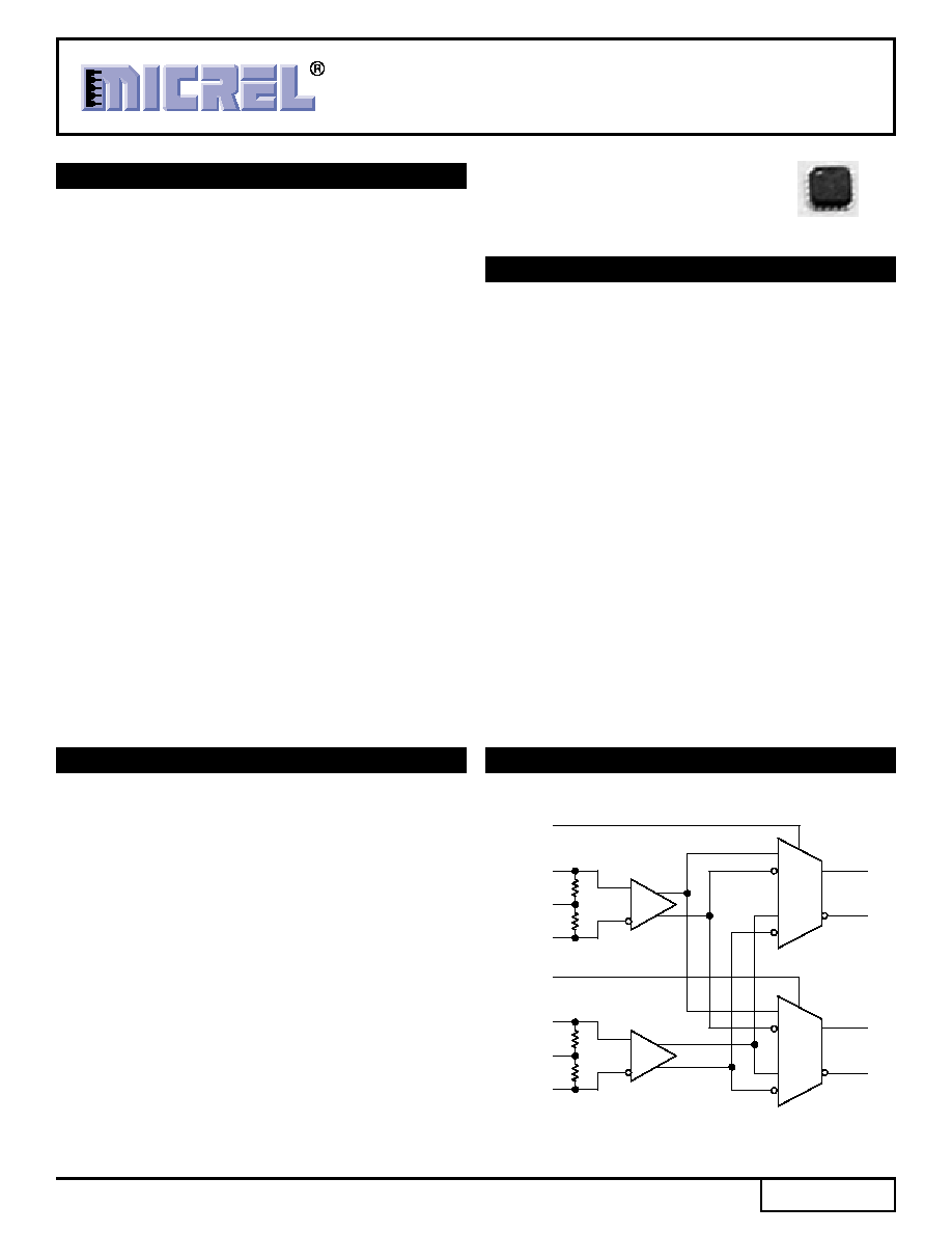
The SY58023U is a 2.5V/3.3V precision, high-speed, fully
differential CML 2
◊
2 crosspoint switch. The SY58023U is
optimized to provide two identical output copies with less
than 20ps of skew and ultra-low jitter. It can route clock
signals as fast as 6GHz or data up to 10.7Gbps.
The differential input includes Micrel's unique, 3-pin input
termination architecture that allows the SY58023U to directly
interface to LVPECL, LVDS, and CML differential signals
(AC- or DC-coupled) as small as 100mV (200mV
pp
) without
any level-shifting or termination resistor networks in the signal
path. The CML outputs features 400mV typical swing into
50
loads, and provide an extremely fast rise/fall time
guaranteed to be less than 60ps.
The SY58023U operates from a +2.5V
±
5% supply or
+3.3V
±
10% supply and is guaranteed over the full industrial
temperature range (≠40
∞
C to +85
∞
C). For applications that
require high speed dual CML switches, consider the
SY58024U. The SY58023U is part of Micrel's high-speed,
Precision Edge
Æ
product line.
Data sheets and support documentation can be found on
Micrel's website at www.micrel.com.
Precision Edge is a registered trademark of Micrel , Inc.
MicroLeadFrame and MLF are trademarks of Amkor Technology, Inc.
Precision Edge
Æ
IN0
/IN0
Q1
/Q1
Q0
/Q0
V
T0
50
50
IN1
/IN1
V
T1
50
50
SEL0
(TTL/CMOS)
SEL1
(TTL/CMOS)
0
1
0
1
FUNCTIONAL BLOCK DIAGRAM
APPLICATIONS
s
Gigabit Ethernet data/clock routing
s
SONET data/clocking routing
s
Switch fabric clock routing
s
Redundant switchover
s
Backplane redundancy
2
Precision Edge
Æ
SY58023U
Micrel, Inc.
M9999-062205
hbwhelp@micrel.com or (408) 955-1690
PACKAGE/ORDERING INFORMATION
Pin Number
Pin Name
Pin Function
1, 2,
IN0, /IN0,
Differential Signal Input: Each pin of this pair internally terminates with 50
to the VT pin.
3, 4
/IN1, IN1
Note that this input will default to an indeterminate state if left open.
See "Input Interface Applications" section.
16, 5
VT0, VT1
Input Termination Center-Tap: Each input terminates to this pin. The VT pin provides a
center-tap for each input (IN, /IN) to a termination network for maximum interface
flexibility. See "Input Interface Applications" section.
15, 6
SEL0, SEL1
Select Input: TTL/CMOS select input control that selects inputs IN0, or IN1. Note that this
input is internally connected to a 25k
pull-up resistor and will default to a logic High
state if left open.
7, 14
GND,
Ground. Exposed pad must be connected to a ground plane that is the same potential as
(Exposed Pad)
the device ground pin.
8, 13
VCC
Positive Power Supply: Bypass with 0.1
µ
F
0.01
µ
F low ESR capacitors as close to the
pins as possible.
12, 11, 10, 9
Q0, /Q0, /Q1, Q1
CML Differential Output Pairs: Differential buffered output copy of the selected input
signal. The CML output swing is typically 400mV across 100
. Unused output pairs may
be left floating with no impact on jitter. See "CML Output Termination" section.
PIN DESCRIPTION
13
14
15
16
12
11
10
9
1
2
3
4
8
7
6
5
IN0
/IN0
/IN1
IN1
Q0
/Q0
/Q1
Q1
VT0
SEL0
GND
VCC
VT1
SEL1
GND
VCC
16-Pin MLFTM (MLF-16)
SEL0
SEL1
Q0
Q1
L
L
IN0
IN0
L
H
IN0
IN1
H
L
IN1
IN0
H
H
IN1
IN1
TRUTH TABLE
Ordering Information
(1)
Package
Operating
Package
Lead
Part Number
Type
Range
Marking
Finish
SY58023UMI
MLF-16
Industrial
023U
Sn-Pb
SY58023UMITR
(2)
MLF-16
Industrial
023U
Sn-Pb
SY58023UMG
(3)
MLF-16
Industrial
023U with
Pb-Free
Pb-Free bar-line indicator
NiPdAu
SY58023UMGTR
(2, 3)
MLF-16
Industrial
023U with
Pb-Free
Pb-Free bar-line indicator
NiPdAu
Notes:
1. Contact factory for die availability. Dice are guaranteed at T
A
= 25
∞
C, DC electricals only.
2. Tape and Reel.
3. Pb-Free package recommended for new designs.
3
Precision Edge
Æ
SY58023U
Micrel, Inc.
M9999-062205
hbwhelp@micrel.com or (408) 955-1690
Absolute Maximum Ratings
(1)
Supply Voltage (V
CC
) .................................. ≠0.5V to +4.0V
Input Voltage (V
IN
) ......................................... ≠0.5V to V
CC
CML Output Voltage (V
OUT
) ......... V
CC
≠1.0V to V
CC
+0.5V
Current (V
T
)
Source or Sink Current on V
T
pin ...................
±
100mA
Input Current (V
T
)
Source or Sink Current on IN, /IN .....................
±
50mA
Lead Temperature (soldering, 20 sec.) ..................... 260
∞
C
Storage Temperature (T
S
) ........................... ≠65
∞
C +150
∞
C
Operating Ratings
(2)
Supply Voltage (V
CC
) ............................ +2.375V to +3.60V
Ambient Temperature (T
A
) ......................... ≠40
∞
C to +85
∞
C
Package Thermal Resistance
(3)
MLFTM
(
JA
)
Still-Air ............................................................. 60
∞
C/W
500lfpm ............................................................ 54
∞
C/W
MLFTM
(
JB
)
Junction-to-board ............................................ 38
∞
C/W
T
A
= ≠40
∞
C to +85
∞
C.
Symbol
Parameter
Condition
Min
Typ
Max
Units
V
CC
Power Supply Voltage
2.5V nominal
2.375
2.5
2.625
V
3.3V nominal
3.0
3.3
3.60
V
I
CC
Power Supply Current
V
CC
= max., current through internal
100
130
mA
50
source termination resistor included.
V
IH
Input HIGH Voltage
IN, /IN; Note 5
V
CC
≠1.6
V
CC
V
V
IL
Input LOW Voltage
IN, /IN
0
V
IH
≠0.1
V
V
IN
Input Voltage Swing
IN, /IN; see Figure 1a.
0.1
1.7
V
V
DIFF_IN
Differential Input Swing
IN, /IN; see Figure 1b.
0.2
V
R
IN
IN-to-V
T
Resistance
40
50
60
IN to V
T
1.28
V
DC ELECTRICAL CHARACTERISTICS
(4)
V
CC
= 2.5V
±
5% or 3.3V
±
10%; T
A
= -40
∞
C to 85
∞
C
Symbol
Parameter
Condition
Min
Typ
Max
Units
V
IH
Input HIGH Voltage
2.0
V
V
IL
Input LOW Voltage
0.8
V
I
IH
Input HIGH Current
40
µ
A
I
IL
Input LOW Current
≠300
µ
A
Notes:
1. Permanent device damage may occur if ratings in the "Absolute Maximum Ratings" section are exceeded. This is a stress rating only and functional
operation is not implied for conditions other than those detailed in the operational sections of this data sheet. Exposure to absolute maximum ratings
conditions for extended periods may affect device reliability.
2. The data sheet limits are not guaranteed if the device is operated beyond the operating ratings.
3. Thermal performance assumes exposed pad is soldered (or equivalent) to the device's most negative potential (GND) on the PCB.
JA
uses 4-layer
in still-air, unless otherwise stated.
4. The circuit is designed to meet the DC specifications shown in the above table after thermal equilibrium has been established.
5. V
IH
(min.) not lower than 1.2V.
LVTTL/CMOS DC ELECTRICAL CHARACTERISTICS
(4)
4
Precision Edge
Æ
SY58023U
Micrel, Inc.
M9999-062205
hbwhelp@micrel.com or (408) 955-1690
AC ELECTRICAL CHARACTERISTICS
(7)
V
CC
= +3.3V
±
10% or +2.5V
±
5%; R
L
= 100
across each output pair; T
A
= ≠40
∞
C to +85
∞
C, unless otherwise stated.
Symbol
Parameter
Condition
Min
Typ
Max
Units
V
OH
Output HIGH Voltage
Q0, /Q0; Q1, /Q1
V
CC
≠0.020
V
CC
V
V
OUT
Output Voltage Swing
Q0, /Q0; Q1, /Q1; see Figure 1a.
325
400
500
mV
V
DIFF_OUT
Differential Voltage Swing
Q0, /Q0; Q1, /Q1; see Figure 1b.
650
800
1000
mV
R
OUT
Output Source Impedance
Q0, /Q0; Q1, /Q1
40
50
60
Notes:
6. The circuit is designed to meet the DC specifications shown in the above table after thermal equilibrium has been established
CML OUTPUT DC ELECTRICAL CHARACTERISTICS
(6)
V
CC
= 2.5V
±
5% or 3.3V
±
10%; R
L
= 100
across each output pair; T
A
= ≠40
∞
C to +85
∞
C, unless otherwise stated.
Symbol
Parameter
Condition
Min
Typ
Max
Units
f
MAX
Maximum Operating Frequency
V
IN
100mV; V
OUT
200mV
Clock
6
GHz
NRZ Data
10.7
Gbps
t
pd
Propagation Delay
IN-to-Q
135
285
ps
SEL-to-Q
100
400
ps
t
SKEW
Channel-to-Channel Skew
(Within Bank)
Note 8
20
ps
Part-to-Part Skew
Note 9
75
ps
t
JITTER
Clock
Cycle-to-Cycle Jitter
Note 10
1
ps
RMS
Total Jitter
Note 11
10
ps
PP
Data
Random Jitter
Note 12
1
ps
RMS
Deterministic Jitter
Note 13
10
ps
PP
Crosstalk Induced Jitter
(Adjacent Channel)
Note 14
0.7
ps
RMS
t
r
, t
f
Output Rise/Fall Time
20% to 80%, at full swing.
25
60
ps
Notes:
7.
Measured with 100mV input swing. High frequency AC-parameters are guaranteed by design and characterization.
8.
Skew is measured between outputs of the same bank under identical transitions.
9.
Skew is defined for two parts with identical power supply voltages at the same temperature and with no skew of the edges at the respective inputs.
10. Cycle-to-cycle jitter definition: The variation of periods between adjacent cycles, T
n
≠T
n≠1
where T is the time between rising edges of the output
signal.
11. Total jitter definition: With an ideal clock input of frequency
f
MAX
, no more than one output edge in 10
12
output edges will deviate by more than
the specified peak-to-peak jitter value.
12. Random jitter is measured with a K28.7 comma detect character pattern, measured at 2.5Gbps≠3.2Gbps.
13. Deterministic jitter is measured at 2.5Gbps≠3.2Gbps with both K28.5 and 2
23
≠1 PRBS pattern.
14. Crosstalk induced jitter is defined as the added jitter that results from signals applied to two adjacent channels. It is measured at the output while
applying similar, differential clock frequencies that are asynchronous with respect to each other at inputs.
5
Precision Edge
Æ
SY58023U
Micrel, Inc.
M9999-062205
hbwhelp@micrel.com or (408) 955-1690
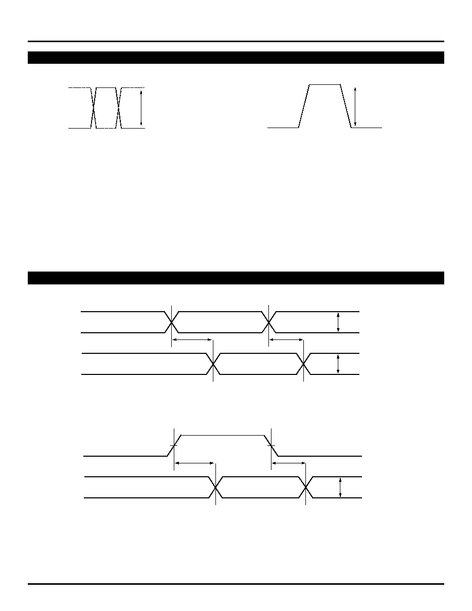
TIMING DIAGRAM
/IN
IN
/Q
Q
t
pd
t
pd
V
OUT
= 400mV (typ.)
(50
load)
V
OUT
= 400mV (typ.)
(50
load)
Figure 2a. AC Timing Diagram IN-to-Q
SEL
/Q
Q
t
pd
t
pd
V
CC
/2
V
CC
/2
IN0, /IN1 = LOW, /IN0, IN1 = HIGH
V
OUT
= 400mV (typ.)
(50
load)
Figure 2b. AC Timing Diagram SEL-to-Q
V
DIFF_IN
,
V
DIFF_OUT
(Typ. 800mV)
Figure 1b. Differential Voltage Swing
V
IN
,
V
OUT
Typ. 400mV
Figure 1a. Single-Ended Voltage Swing
SINGLE-ENDED AND DIFFERENTIAL SWINGS