1
Precision EdgeTM
SY58030U
Micrel
M9999-040604
hbwhelp@micrel.com or (408) 955-1690
ULTRA PRECISION, 400mV
DIFFERENTIAL LVPECL 4:1 MUX with 1:2
FANOUT and INTERNAL TERMINATION
Precision EdgeTM
SY58030U
Rev.: A
Amendment: /0
Issue Date:
April 2004
DESCRIPTION
s
Selects 1 of 4 differential inputs
s
Provides two copies of the selected input
s
Guaranteed AC performance over temperature and
voltage:
∑ DC-to- > 10.7Gbps data rate throughput
∑ < 340ps IN-to-Out t
pd
∑ < 80ps t
r
/ t
f
times
s
Ultra low-jitter design:
∑ < 10ps
pp
total jitter (clock)
∑ < 1ps
rms
random jitter
∑ < 10ps
pp
deterministic jitter
∑ < 0.7ps
rms
crosstalk-induced jitter
s
Unique patended input design minimizes crosstalk
s
Accepts an input signal as low as 100mV
s
Unique patended input termination and V
T
pin
accepts DC-coupled and AC-coupled inputs (CML,
LVPECL, LVDS)
s
400mV 100k LVPECL output swing
s
Power supply 2.5V
±
5% or 3.3V
±
10%
s
≠40
∞
C to +85
∞
C temperature range
s
Available in 32-pin (5mm
◊◊
◊◊
◊
5mm) MLFTM package
FEATURES
APPLICATIONS
s Redundant clock and/or data distribution
s
All SONET/SDH clock/data distribution
s
Loopback
s
All Fibre Channel distribution
s
All Gigabit Ethernet clock and/or data distribution
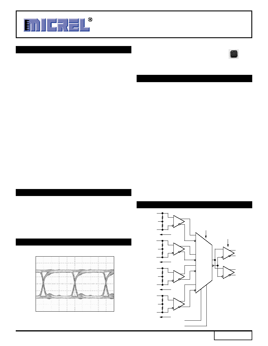
The SY58030U is a 2.5V/3.3V precision, high-speed, 4:1
differential multiplexer with 400mV LVPECL outputs, capable
of handling clocks up to 7GHz and data streams up to
10.7Gbps. In addition, a 1:2 fanout buffer provides two copies
of the selected input.
The differential input includes Micrel's unique, 3-pin input
termination architecture that allows customers to interface to
any differential signal (AC- or DC-coupled) as small as 100mV
without any level shifting or termination resistor networks in
the signal path. The result is a clean, stub-free, low-jitter
interface solution. The outputs are 400mV LVPECL (100k
temperature compensated) with extremely fast rise/fall times
guaranteed to be less than 80ps.
The SY58030U operates from a 2.5V
±
5% supply or a
3.3V
±
10% supply and is guaranteed over the full industrial
temperature range of ≠40
∞
C to +85
∞
C. For applications that
require CML outputs, consider the SY58028U. For 800mV
LVPECL outputs, consider the SY58029U. The SY58030U is
part of Micrel's high-speed, Precision EdgeTM product line.
All support documentation can be found on Micrel's web
site at www.micrel.com.
TYPICAL PERFORMANCE
Precision Edge is a trademark of Micrel, Inc.
Micro
LeadFrame and MLF are trademarks of Amkor Technology, Inc.
Precision EdgeTM
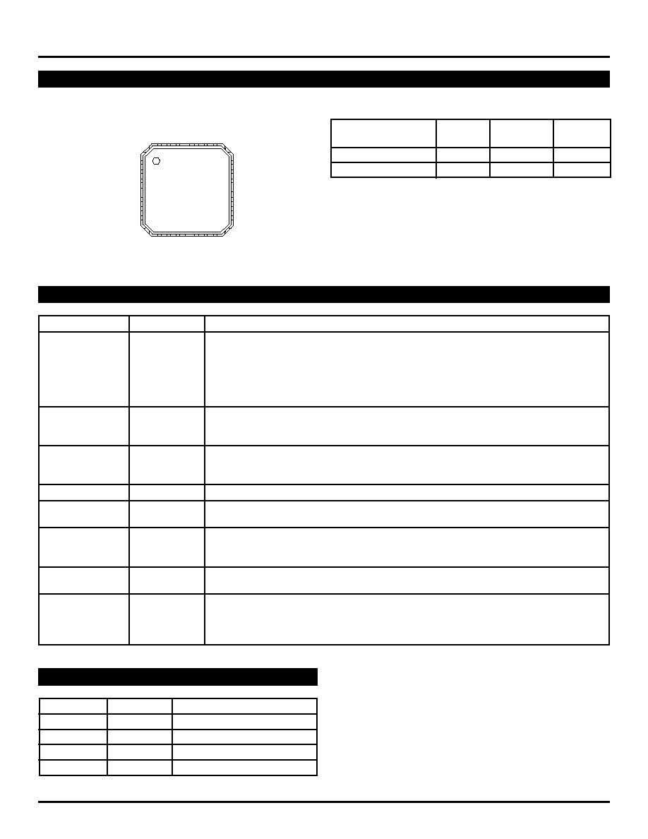
FUNCTIONAL BLOCK DIAGRAM
IN0
/IN0
V
T0
50
50
IN1
/IN1
V
T1
50
50
Q0
/Q0
0
1
MUX
4:1 MUX
1:2 Fanout
V
REF-AC0
IN2
/IN2
V
T2
50
50
V
REF-AC2
V
REF-AC1
2
IN3
/IN3
V
T3
50
50
V
REF-AC3
3
SEL0 (CMOS/TTL)
SEL1 (CMOS/TTL)
Q1
/Q1
2.5Gbps Output (2
23
--1 PRBS)
TIME (100ps/div.)
Output Swing
(100mV/div
.)
2
Precision EdgeTM
SY58030U
Micrel
M9999-040604
hbwhelp@micrel.com or (408) 955-1690
PACKAGE/ORDERING INFORMATION
Ordering Information
(1)
Package
Operating
Package
Part Number
Type
Range
Marking
SY58030UMI
MLF-32
Industrial
SY58030U
SY58030UMITR
(2)
MLF-32
Industrial
SY58030U
Notes:
1. Contact factory for die availability. Die are guaranteed at T
A
= 25
∞
C,
DC electricals only.
2. Tape and Reel.
1
2
3
4
5
6
7
8
24
23
22
21
20
19
18
17
9 10 11 12 13 14 15 16
32 3130 29 28 27 26 25
IN0
VT0
VREF-AC0
/IN0
IN1
VT1
VREF-AC1
/IN1
GND
VCC
Q1
/Q1
VCC
NC
SEL1
VCC
/IN2
IN3
VT3
VREF-AC3
/IN3
VREF-AC2
VT2
IN2
VCC
Q0
/Q0
VCC
GND
NC
SEL0
VCC
32-Pin MLFTM (MLF-32)
Pin Number
Pin Name
Pin Function
1, 4
IN0, /IN0
Differential Input: Each pair accepts AC- or DC-coupled signals as small as 100mV.
5, 8
IN1, /IN1
Each pin of a pair internally terminates to a V
T
pin through 50
. Note that these
25, 28
IN2, /IN2
inputs will default to an indeterminate state if left open. If an input is not used, connect one
29, 32
IN3, /IN3
end of the differential pair to ground through a 1k
resistor, and leave the other end to
V
CC
through a 825
resistor. Unused V
T
and V
REF-AC
pins may also be left floating.
Please refer to the "Input Interface Applications" section for more details.
2, 6, 26, 30
VT0, VT1
Input Termination Center-Tap: Each side of the differential input pair terminates to a V
T
VT2, VT3
pin. The V
T
pins provide a center-tap to the termination network for maximum
interface flexibility. See "Input Interface Applications" section for more details.
15, 18
SEL0, SEL1
This Single-Ended TTL/CMOS compatible input selects the inputs to the multiplexer. Note
that this input is internally connected to a 25k
pull-up resistor and will default to a logic
HIGH state if left open. Input logic threshold is V
CC
/2. See "Truth Table" for select control.
14, 19
NC
No Connect.
10, 13, 16
VCC
Positive Power Supply: Bypass with 0.1
µ
F
0.01
µ
F low ESR capacitors.
17, 20, 23
11, 12
/Q0, Q0
Differential Outputs: These 100k compatible (internally temperature compensated)
21, 22
/Q1, Q1
LVPECL output pairs are copies of the selected input. Unused output pairs may be left
floating. See "Output Interface" for termination guidelines.
9, 24
GND,
Ground. Ground pin and exposed pad must be connected to the same ground plane.
Exposed Pad
3, 7, 27, 31
VREF-AC0
Reference Voltage: This reference output is equivalent to V
CC
≠1.4V. It is used for
VREF-AC1
AC-coupled inputs. When interfacing to AC input signals, connect V
REF-AC
directly to the
VREF-AC2
V
T
pin and bypass with a 0.01
µ
F low ESR capacitor to V
CC
. See "Input Interface
VREF-AC3
Applications" section. Maximum current sink/source is 0.5mA.
PIN DESCRIPTION
TRUTH TABLE
SEL0
SEL1
0
0
IN0 Input Selected
0
1
IN1 Input Selected
1
0
IN2 Input Selected
1
1
IN3 Input Selected
3
Precision EdgeTM
SY58030U
Micrel
M9999-040604
hbwhelp@micrel.com or (408) 955-1690
Absolute Maximum Ratings
(1)
Power Supply Voltage (V
CC
) ...................... ≠0.5V to +4.0V
Input Voltage (V
IN
) ......................................... ≠0.5V to V
CC
LVPECL Output Current (I
OUT
)
Continuous ............................................................. 50mA
Surge .................................................................... 100mA
Termination Current
(3)
Source or sink current on V
T
pin ........................
±
100mA
Input Current
Source or sink current on IN, /IN pin ....................
±
50mA
Lead Temperature (soldering, 10 sec.) ..................... 265
∞
C
Storage Temperature Range (T
S
) ........... ≠65
∞
C to +150
∞
C
Operating Ratings
(2)
Power Supply Voltage (V
CC
) ............... +2.375V to +2.625V
............................................................ +3.0V to +3.6V
Ambient Temperature Range (T
A
) ............. ≠40
∞
C to +85
∞
C
Package Thermal Resistance
(4)
MLFTM (
JA
)
Still-Air ............................................................. 35
∞
C/W
MLFTM (
JB
)
Junction-to-Board .............................................. 2
∞
C/W
T
A
= -40
∞
C to 85
∞
C, unless otherwise stated.
Symbol
Parameter
Condition
Min
Typ
Max
Units
V
CC
Power Supply Voltage
V
CC
= 2.5V
2.375
2.5
2.625
V
V
CC
= 3.3V
3.0
3.3
3.6
V
I
CC
Power Supply Current
No load, max. V
CC
120
150
mA
R
DIFF_IN
Differential Input Resistance (IN-to-/IN)
80
100
120
R
IN
Input Resistance (IN-to-V
T
, /IN-to-V
T
)
40
50
60
V
IH
Input HIGH Voltage (IN-to-/IN)
Note 6
V
CC
≠1.6
V
CC
V
V
IL
Input LOW Voltage (IN-to-/IN)
0
V
IH
≠0.1
V
V
IN
Input Voltage Swing (IN-to-/IN)
See Figure 1a.
0.1
1.7
V
V
DIFF_IN
Differential Input Voltage Swing (IN-to-/IN)
See Figure 1b.
200
mV
V
T
IN
Max Input Voltage (IN-to-V
T
)
1.28
V
V
REF-AC
Reference Voltage
V
CC
≠1.3 V
CC
≠1.2 V
CC
≠1.1
V
Notes:
1. Permanent device damage may occur if ratings in the "Absolute Maximum Ratings" section are exceeded. This is a stress rating only and functional
operation is not implied at conditions other than those detailed in the operational sections of this data sheet. Exposure to absolute maximum ratings
conditions for extended periods may affect device reliability.
2. The data sheet limits are not guaranteed if the device is operated beyond the operating ratings.
3. Due to the limited drive capability, use for input of the same package only.
4. Thermal performance assumes exposed pad is soldered (or equivalent) to the device's most negative potential (GND) on the PCB.
JB
uses 4-layer
JA
in still air number unless otherwise stated.
5. The circuit is designed to meet the DC specifications shown in the above table after thermal equilibrium has been established.
6. V
IH
(min), not lower than 1.2V.
DC ELECTRICAL CHARACTERISTICS
(5)
4
Precision EdgeTM
SY58030U
Micrel
M9999-040604
hbwhelp@micrel.com or (408) 955-1690
V
CC
= 2.5V
±
5% or 3.3V
±
10%; T
A
= ≠40
∞
C to +85
∞
C; R
L
= 50
to V
CC
--2V, unless otherwise stated.
Symbol
Parameter
Condition
Min
Typ
Max
Units
V
OH
Output HIGH Voltage
V
CC
≠1.145
V
CC
≠0.895
V
V
OL
Output LOW Voltage
V
CC
≠1.545
V
CC
≠1.295
V
V
OUT
Output Voltage Swing
See Figure 1a.
150
400
mV
V
DIFF_OUT
Differential Output Voltage Swing
See Figure 1b.
300
800
mV
LVPECL OUTPUT DC ELECTRICAL CHARACTERISTICS
(7)
V
CC
= 2.5V
±
5% or 3.3V
±
10%; T
A
= ≠40
∞
C to +85
∞
C, unless otherwise stated.
Symbol
Parameter
Condition
Min
Typ
Max
Units
V
IH
Input HIGH Voltage
SEL0, SEL1
2.0
V
V
IL
Input LOW Voltage
SEL0, SEL1
0.8
V
I
IH
Input High Current
40
µ
A
I
IL
Input Low Current
≠300
µ
A
Note:
7. The circuit is designed to meet the DC specifications shown in the above table after thermal equilibrium has been established.
LVTTL/CMOS DC ELECTRICAL CHARACTERISTICS
(7)
5
Precision EdgeTM
SY58030U
Micrel
M9999-040604
hbwhelp@micrel.com or (408) 955-1690
SINGLE-ENDED AND DIFFERENTIAL SWINGS
V
IN
,
V
OUT
400mV (Typ.)
Figure 1a. Single-Ended Voltage Swing
V
DIFF_IN
,
V
DIFF_OUT
800mV (Typ.)
Figure 1b. Differential Voltage Swing
V
CC
= 2.5V
±
5% or 3.3V
±
10%; R
L
= 50
to V
CC
≠2V; T
A
= ≠40
∞
C to +85
∞
C, V
IN
100mV, unless otherwise stated.
Symbol
Parameter
Condition
Min
Typ
Max
Units
f
MAX
Maximum Operating Frequency
NRZ Data
10.7
Gbps
V
OUT
200mV
Clock
7
GHz
t
pd
Propagation Delay (Diff)
(IN to Q)
V
IN
100mV
170
260
340
ps
(SEL to Q)
100
500
ps
t
pd
Tempco
Differential Propagation Delay
115
fs/
∞
C
Temperature Coefficient
t
SKEW
Output-to-Output Skew
Note 9
7
20
ps
Part-to-Part Skew
Note 10
50
ps
t
JITTER
Data
Random Jitter
Note 11
2.5Gbps to 3.2Gbps
1
ps
pp
Deterministic Jitter
Note 12
2.5Gbps to 3.2Gbps
10
ps
pp
Clock
Cycle-to-Cycle Jitter
Note 13
1
ps
rms
Total Jitter
Note 14
10
ps
pp
Crosstalk Induced Jitter
Note 15
0.7
ps
rms
(Adjacent Channel)
t
r
, t
f
Output Rise/Fall Time
20% to 80%, Full output swing
20
55
80
ps
Notes:
8. High frequency AC electricals are guaranteed by design and characterization.
9. Output-to-output skew is measured between outputs under identical input conditions.
10. Part-to-part skew is defined for two parts with identical power supply voltages at the same temperature and with no skew of the edges at the
respective inputs.
11. Random jitter is measured with a K28.7 comma detect character pattern, measured at 2.5Gbps to 3.2Gbps.
12. Deterministic jitter is measured at 2.5Gpbs to 3.2Gbps with both K28.5 and 2
23
≠1 PRBS pattern.
13. Cycle-to-cycle jitter definition: the variation of periods between adjacent cycles, T
n
-T
n≠1
, where T is the time between rising edges of the output
signal.
14. Total jitter definition: with an ideal clock input of frequency
f
MAX
, no more than one output edge in 10
12
output edges will deviate by more than the
specified peak-to-peak jitter value.
15. Crosstalk is measured at the output while applying two similar clock frequencies that are asynchronous with respect to each other at the inputs.
AC ELECTRICAL CHARACTERISTICS
(8)