 | –≠–ª–µ–∫—Ç—Ä–æ–Ω–Ω—ã–π –∫–æ–º–ø–æ–Ω–µ–Ω—Ç: SY58052U | –°–∫–∞—á–∞—Ç—å:  PDF PDF  ZIP ZIP |
1
Precision EdgeTM
SY58052U
Micrel
M9999-050404
hbwhelp@micrel.com or (408) 955-1690
DESCRIPTION
s
Resynchronizes data to a reference clock
s
Guaranteed AC performance over temperature and
voltage:
∑ DC-to > 10.7Gbps data rate throughput
∑ DC-to > 7GHz clock f
MAX
∑ < 190ps Any In-to-Out t
pd
∑ t
r
/ t
f
< 60ps
s
Ultra low-jitter design:
∑ < 1ps
rms
random jitter
∑ < 10ps
pp
deterministic jitter
∑ < 10ps
pp
total jitter (clock)
s
Internal 50
input termination
s
Unique input termination and V
T
pin accepts DC-
coupled and AC-coupled inputs (CML, PECL)
s
Internal 50
output source termination
s
400mV CML output swing
s
Power supply 2.5V
±
5% or 3.3V
±
10%
s
≠40
∞
C to 85
∞
C temperature range
s
Available in a 16-pin (3mm
◊◊
◊◊
◊
3mm) MLFTM package
FEATURES
ULTRA-PRECISION CML DATA AND
CLOCK SYNCHRONIZER W/ INTERNAL
INPUT AND OUTPUT TERMINATION
Precision EdgeTM
SY58052U
APPLICATIONS
s
Data communication systems
s
Serial OC-192, OC-192+FEC data-to-clock
realignment
s
Parallel 10Gbps for OC768
s
All SONET OC-3 -- OC-768 applications
s
All Fibre Channel applications
s
All GigE applications
Rev.: A
Amendment: /0
Issue Date:
May 2004
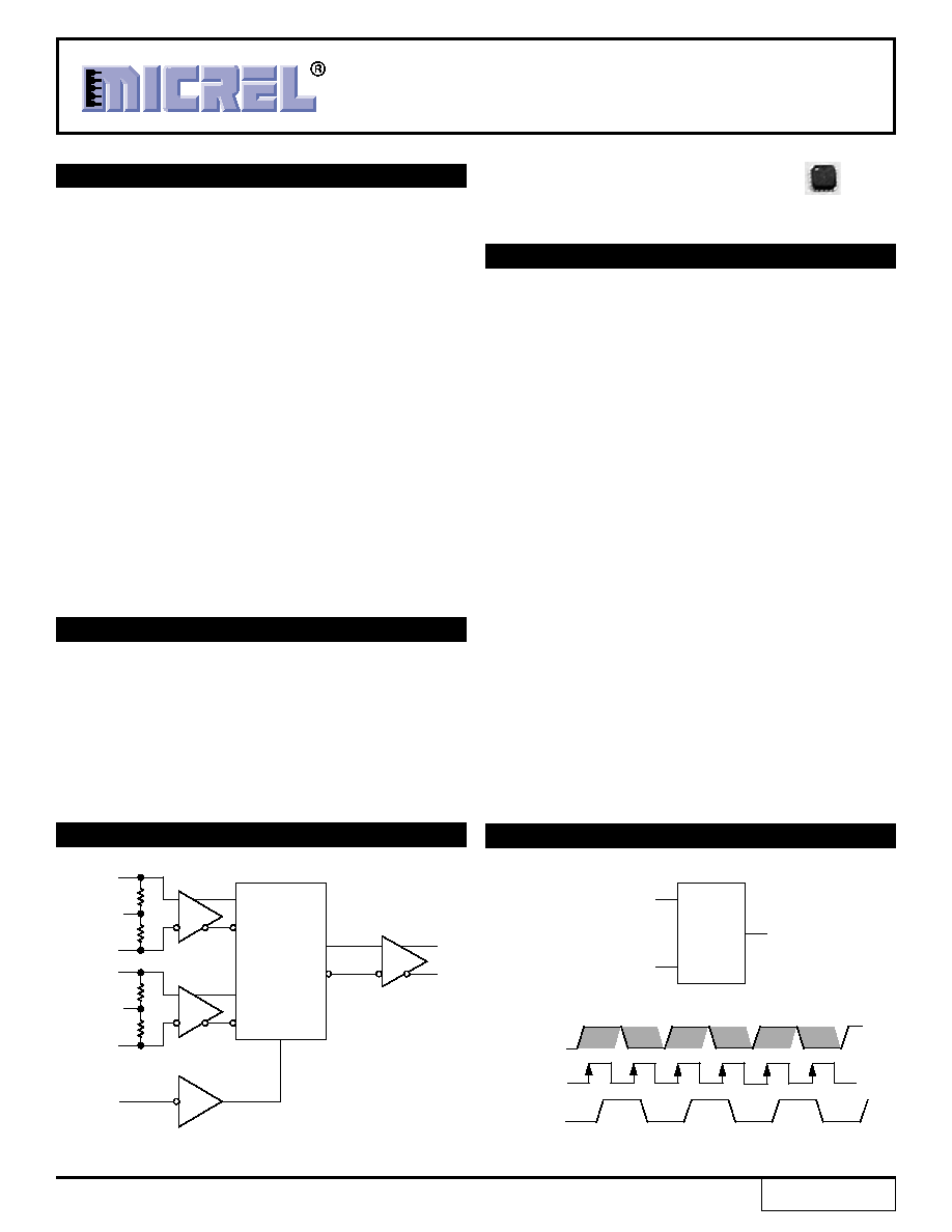
The SY58052U is an ultra-fast, precision, low jitter data-
to-clock resynchronizer with a guaranteed maximum data
and clock throughput of 10.7Gbps or 7GHz, respectively.
The SY58052U is an ideal solution for backplane retiming
or retiming after the data passes through long trace lengths.
Serial data comes into the data input, and the CML output
is synchronous to the input reference clock's rising edge.
The SY58052U differential inputs include a unique,
internal termination design that allows access to the
termination network through a V
T
pin. This feature allows
the device to easily interface to different logic standards,
both AC- and DC-coupled, without external resistor-bias
and termination networks. The result is a clean, stub-free,
low-jitter interface solution. The differential CML output is
optimized for 50
environments with internal 50
source
termination and a 400mV output swing.
The SY58052U operates from a 2.5V or 3.3V supply and
is guaranteed over the full industrial temperature range
(≠40
∞
C to +85
∞
C). The SY58052U is part of a Micrel's
Precision EdgeTM product family.
All support documentation can be found on Micrel's web
site at www.micrel.com.
Precision Edge is a trademark of Micrel, Inc. and AnyGate is a registered trademark of Micrel, Inc.
Micro
LeadFrame and MLF are trademarks of Amkor Technology, Inc.
Precision EdgeTM
FUNCTIONAL BLOCK DIAGRAM
TYPICAL APPLICATION
V
TCLK
CLK
/CLK
V
TD
DATA
/DATA
Q
/Q
50
50
50
50
/RESET
DATA
/DATA
CLK
/CLK
R
Q
/Q
DATA
CLK
Q
Data from
Backplane
(Uncertain timing)
Clock from Backplane
Retimed
Data
SY58052U
DATA IN
CLK
Q OUT
(Retimed)
2
Precision EdgeTM
SY58052U
Micrel
M9999-050404
hbwhelp@micrel.com or (408) 955-1690
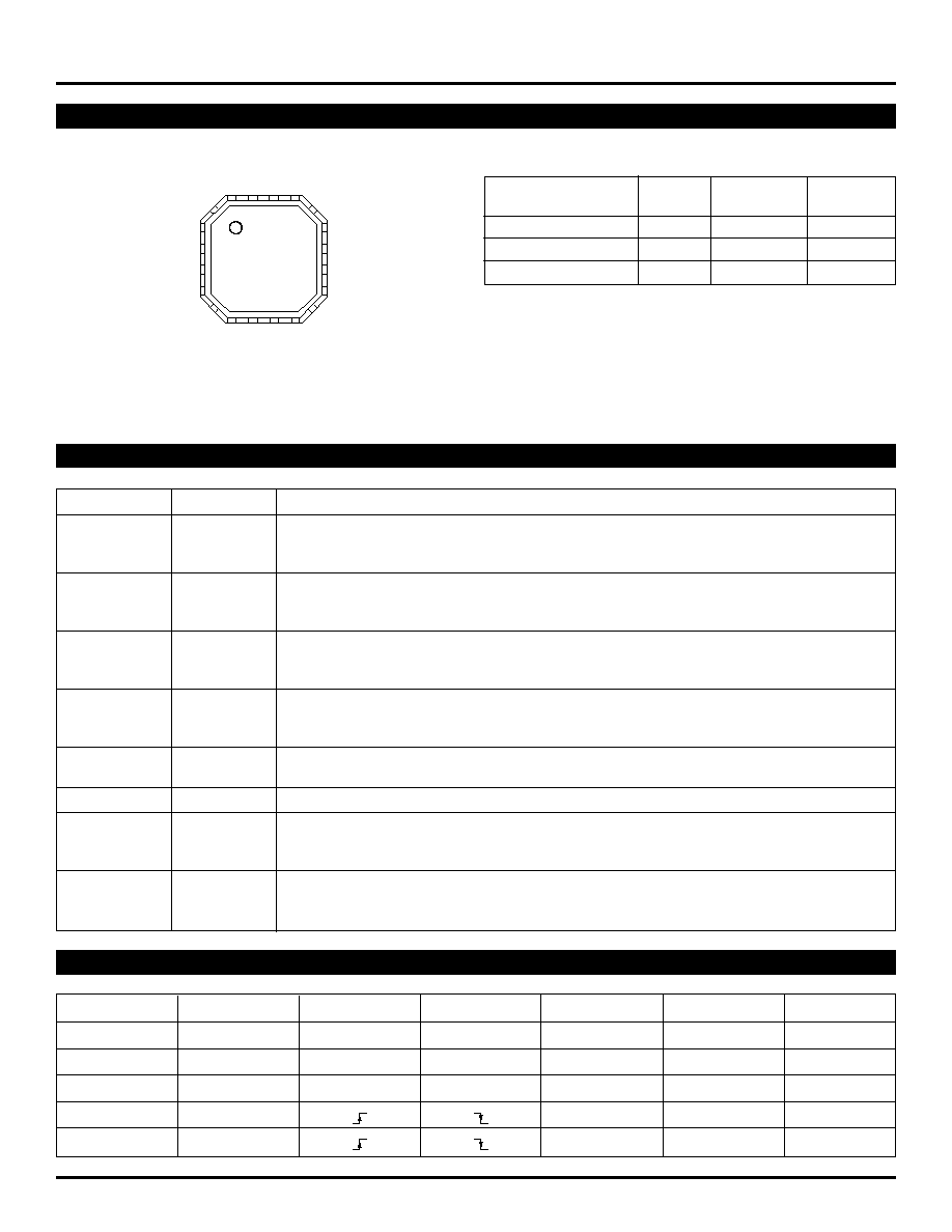
PACKAGE/ORDERING INFORMATION
PIN DESCRIPTION
Ordering Information
(1)
Package
Operating
Package
Part Number
Type
Range
Marking
SY58052UMI
DIE
Ambient
--
SY58052UMI
MLF-16
Industrial
052U
SY58052UMITR
(2)
MLF-16
Industrial
052U
Notes:
1. Contact factory for die availability. Die is guaranteed at T
A
= 25
∞
C, DC
electricals only.
2. Tape and Reel.
1
2
3
4
12
11
10
9
16 15 14 13
5
6
7
8
CLK
/CLK
DATA
/DATA
Q
GND
GND
/Q
VCC
GND
GND
VTCLK
VCC
GND
/RESET
VTDA
T
A
16-Pin MLFTM (MLF-16)
Pin Number
Pin Name
Pin Function
1, 2
CLK, /CLK
Differential Input: This input pair is the clock signal that re-times the data signal at DATA, /DATA.
Each pin of this pair internally terminates to the V
TCLK
pin to 50
. Note that this input will
default to an indeterminate state if left open. See "Input Interface Applications" section.
3, 4
DATA, /DATA
Differential Input: This input pair is the signal to be synchronized by the CLK, /CLK signal. Each
pin of this pair internally terminates to the V
TD
pin to 50
. Note that this input will default to an
indeterminate state if left open. See "Input Interface Applications" section.
5
VTData
Input Termination Center-Tap: Each of the two inputs, DATA, /DATA terminates to this pin. The
VTData pin provides a center-tap to a termination network for maximum interface flexibility.
See "Input Interface Applications" section.
6
/RESET
TTL/CMOS-Compatible Input: The /RESET input asynchronously forces the Q output to a logic
"0" state whenever it is active low. Possible state changes due to rising edges on CLK, /CLK are
ignored until /RESET goes inactive high.
7, 10, 11, 14, 15
GND
Ground. Exposed pad must be connected to the same potential as the GND pin.
(Exposed Pad)
8, 13
VCC
Positive Power Supply. Bypass with 0.1
µ
F
0.01
µ
F low ESR capacitors.
12, 9
Q, /Q
Differential Output: This CML output pair is the output of the flip-flop. The Data input is
transferred to the Q output at the rising edge of CLK (falling edge of /CLK). See "Input Interface
Applications" section.
16
VTCLK
Input Termination Center-Tap: Each of the two inputs, CLK, /CLK terminates to this pin. The
VTCLK pin provides a center-tap to a termination network for maximum interface flexibility.
See "Input Interface Applications" section.
DATA
/DATA
CLK
/CLK
/RESET
Q
/Q
X
X
X
X
0
0
1
X
X
0
1
1
Q
N≠1
/Q
N≠1
X
X
1
0
1
Q
N≠1
/Q
N≠1
0
1
1
0
1
1
0
1
1
0
TRUTH TABLES
3
Precision EdgeTM
SY58052U
Micrel
M9999-050404
hbwhelp@micrel.com or (408) 955-1690
Absolute Maximum Ratings
(1)
Supply Voltage (V
CC
) .................................. ≠0.5V to +4.0V
Input Voltage (V
IN
) ......................................... ≠0.5V to V
CC
CML Output Voltage (V
OUT
) ......... V
CC
≠1.0V to V
CC
+5.0V
Termination Current
(3)
Source or Sink Current on V
TD
, V
CLK .......................
±
60mA
Input Current
Source or Sink Current on D, /D, CLK, /CLK .......
±
30mA
Lead Temperature (soldering, 10 sec.) ................... +265
∞
C
Storage Temperature (T
S
) ....................... ≠65
∞
C to +150
∞
C
Operating Ratings
(2)
Supply Voltage (V
CC
) .......................... +2.375V to +2.625V
............................................................ +3.0V to +3.6V
Ambient Temperature (T
A
) ......................... ≠40
∞
C to +85
∞
C
Package Thermal Resistance
(4)
MLFTM
(
JA
)
Still-Air ............................................................. 61
∞
C/W
MLFTM
(
JB
)
Junction-to-Board ............................................ 38
∞
C/W
T
A
= ≠40
∞
C to +85
∞
C, unless otherwise noted.
Symbol
Parameter
Condition
Min
Typ
Max
Units
V
CC
Power Supply
2.375
2.625
V
3.0
3.6
V
I
CC
Power Supply Current
No load, max. V
CC
.
60
90
mA
R
IN
Differential Input Resistance
80
100
120
(D, /D or CLK, /CLK)
V
IH
Input HIGH Voltage
Note 6
1.2
V
CC
V
(D, /D or CLK, /CLK)
V
IL
Input LOW Voltage
Note 6
0
V
IH
≠0.1
V
(D, /D or CLK, /CLK)
V
IN
Input Voltage Swing
Note 6
100
mV
(D, /D or CLK, /CLK)
V
DIFF_IN
Differential Input Voltage Swing
Note 6
200
mV
|D, /D| or |CLK, /CLK|
See Figure 2a.
|I
IN
|
Input Current
Note 6
21
mA
(IN, /IN)
See Figure 2b.
Notes:
1. Permanent device damage may occur if the ratings in the "Absolute Maximum Ratings" section are exceeded. This is a stress rating only and
functional operation is not implied for conditions other than those detailed in the operational sections of this data sheet. Exposure to absolute
maximum ratings conditions for extended periods may affect device reliability.
2. The data sheet limits are not guaranteed if the device is operated beyond the operating ratings.
3. Due to the limited drive capability use for input of the same package only.
4. Package thermal resistance assumes exposed pad is soldered (or equivalent) to the device's most negative potential on the PCB.
JB
uses 4-layer
JA
in still-air, unless otherwise stated.
5. The circuit is designed to meet the DC specifications shown in the above table after thermal equilibrium has been established.
6. Due to the internal termination (see " Input Structures" section) the input current depends on the applied voltages at D, /D and V
TD
inputs, the CLK,
/CLK and V
TCLK
inputs or the S, /S and V
TS
inputs. Do not apply a combination of voltages that causes the input current to exceed the maximum
limit!
DC ELECTRICAL CHARACTERISTICS
(5)
4
Precision EdgeTM
SY58052U
Micrel
M9999-050404
hbwhelp@micrel.com or (408) 955-1690
V
CC
= 2.5V
±
5% or 3.3V
±
10%; R
L
= 100
across output pair or equivalent; T
A
= ≠40
∞
C to +85
∞
C; unless otherwise noted.
Symbol
Parameter
Condition
Min
Typ
Max
Units
f
MAX
Maximum Operating Frequency
10.7
GHz
t
pd
Propagation Delay
(CLK-to-Q)
70
190
ps
t
RESET
Propagation Delay
V
TH
= V
CC
/2
600
ps
(RESET-to-Q)
t
S
Set-Up Time
20
ps
t
H
Hold Time
20
ps
t
RR
Reset Recovery Time
500
ps
t
JITTER
Random Jitter (RJ)
Note 9
1
ps
rms
Deterministic Jitter (DJ)
Note 10
10
ps
pp
Total Jitter (TJ)
10GHz Clock, 1
◊
10
≠12
BER, Note 11
10
ps
pp
10GHz Data, 1
◊
10
≠12
BER, Note 11
14
ps
pp
t
r
, t
f
Rise/Fall Times (20% to 80%)
At full output swing.
20
30
60
ps
Notes:
7. The circuit is designed to meet the DC specifications shown in the above table after thermal equilibrium has been established.
8. Measured with 100mV input swing. See "Timing Diagrams" section for definition of parameters. High-frequency AC-parameters are guaranteed by
design and characterization.
9. RJ is measured with a K28.7 comma detect character pattern, measured at 10.7Gbps and 2.5Gbps.
10. DJ is measured at 10.7Gbps and 2.5Gbps, with both K28.5 and 2
23
≠1 PRBS pattern
11. Total jitter definition: with an ideal clock input frequency of
f
MAX
, no more than one output edge in 10
12
output edges will deviate by more than
the specified peak-to-peak jitter value.
AC ELECTRICAL CHARACTERISTICS
(8)
V
CC
= 2.5V
±
5% or 3.3V
±
10%; T
A
= ≠40
∞
C to +85
∞
C; unless otherwise noted.
Symbol
Parameter
Condition
Min
Typ
Max
Units
V
IH
Input HIGH Voltage
2.0
V
V
IL
Input LOW Voltage
0.8
mV
I
IH
Input HIGH Current
≠125
20
µ
A
I
IL
Input LOW Current
≠300
µ
A
LVTTL/CMOS DC ELECTRICAL CHARACTERISTICS
(7)
V
CC
= 2.5V
±
5% or 3.3V
±
10%; R
L
= 100
across output pair or equivalent; T
A
= ≠40
∞
C to +85
∞
C; unless otherwise noted.
Symbol
Parameter
Condition
Min
Typ
Max
Units
V
OH
Output HIGH Voltage Q, /Q
V
CC
≠0.020
V
CC
V
V
OUT
Output Voltage Swing Q, /Q
See Figure 2a.
325
400
500
mV
V
DIFF_OUT
Differential Output Voltage Swing
See Figure 2b.
650
800
1000
mV
Q, /Q
R
OUT
Output Source Impedance
40
50
60
Q, /Q
CML OUTPUTS DC ELECTRICAL CHARACTERISTICS
(7)
5
Precision EdgeTM
SY58052U
Micrel
M9999-050404
hbwhelp@micrel.com or (408) 955-1690
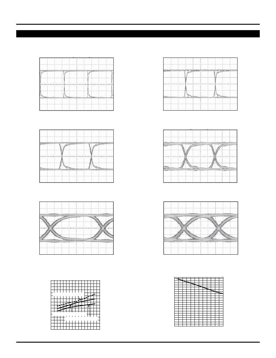
TYPICAL OPERATING CHARACTERISTICS
622Mbps Output
TIME (500ps/div.)
Output Swing
(50mV/div
.)
PRBS
2
23--1
1.25Gbps Output
TIME (200ps/div.)
Output Swing
(50mV/div
.)
PRBS
2
23--1
100
105
110
115
120
125
130
135
140
-60 -40 -20 0
20 40 60 80 100
PROPAGATION DELAY (ps)
TEMPERATURE (
∞
C) (Forced Air)
IN to Q Propagation Delay
vs. Temperature
PECL (800mV Swing)
CML (200mV Swing)
LVDS (400mV Swing)
200
220
240
260
280
300
320
340
360
380
400
420
0
2
4
6
8
10
12
OUTPUT AMPLITUDE (mV)
DATA RATE (Gbps)
Output Amplitude
vs. Data Rate
V
CC
= 3.3V, GND = 0V, CLK = 400mV, D = 400mV, T
A
= 25
∞
C.
2.5Gbps Output
TIME (100ps/div.)
Output Swing
(50mV/div
.)
PRBS
2
23--1
5Gbps Output
TIME (50ps/div.)
Output Swing
(50mV/div
.)
PRBS
2
23--1
7Gbps Output
TIME (20ps/div.)
Output Swing
(50mV/div
.)
PRBS
2
23--1
10.7Gbps Output
TIME (20ps/div.)
Output Swing
(50mV/div
.)
PRBS
2
23--1