 | –≠–ª–µ–∫—Ç—Ä–æ–Ω–Ω—ã–π –∫–æ–º–ø–æ–Ω–µ–Ω—Ç: SY87700AL | –°–∫–∞—á–∞—Ç—å:  PDF PDF  ZIP ZIP |
SY87700AL
Low-Power, 3.3V, 32Mbps to 208Mbps
AnyRate
Æ
Clock and Data Recovery
AnyRate is a registered trademark of Micrel, Inc.
Micrel Inc. ∑ 2180 Fortune Drive ∑ San Jose, CA 95131 ∑ USA ∑ tel +1 (408) 944-0800 ∑ fax + 1 (408) 474-1000 ∑ http://www.micrel.com
November 2006
M9999-111406-B
hbwhelp@micrel.com
or (408) 955-1690
General Description
The SY87700AL is a complete clock recovery and data
retiming integrated circuit for data rates from 32Mbps up
to 208Mbps NRZ. The device is ideally suited for
SONET/SDH/ATM applications and other high-speed
data transmission systems.
Clock recovery and data retiming is performed by
synchronizing the on-chip VCO directly to the incoming
data stream. The VCO center frequency is controlled by
the reference clock frequency and the selected divide
ratio. On-chip clock generation is performed through the
use of a frequency multiplier PLL with a byte rate source
as reference.
The SY87700AL also includes a link fault detection
circuit.
Data sheets and support documentation can be found
on Micrel's web site at:
www.micrel.com
.
AnyRate
Æ
Features
∑ 3.3V power supply
∑ SONET/SDH/ATM compatible
∑ Clock and data recovery from 32Mbps up to
208Mbps NRZ data stream; clock generation from
32Mbps to 208Mbps
∑ Two on-chip PLLs: one for clock generation and
another for clock recovery
∑ Selectable reference frequencies
∑ Differential PECL high-speed serial I/O
∑ Line receiver input: no external buffering needed
∑ Link fault indication
∑ 100K ECL-compatible I/O
∑ Industrial temperature range (≠40∞C to +85∞C)
∑ Low power: fully compatible with Micrel's SY87700V,
but with 30% less power
∑ Available in 32-pin EPAD-TQFP and 28-pin EPAD
SOIC packages, (28-pin SOIC is available, but NOT
recommended for new designs.)
Applications
∑ SONET/SDH/ATM OC-1 and OC-3
∑ Fast Ethernet, SMPTE 259
∑ Proprietary architecture up to 208Mbps
Micrel, Inc.
SY87700AL
November 2006
2
M9999-111406-B
hbwhelp@micrel.com
or (408) 955-1690
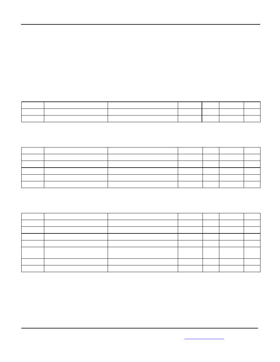
Ordering Information
(1)
Part Number
Package
Type
Operating
Range
Package
Marking
Lead
Finish
SY87700ALZG
(2)
Z28-1 Industrial
SY87700ALZG with
Pb-Free bar-line indicator
NiPdAu
Pb-Free
SY87700ALHG
(2)
H32-1 Industrial
SY87700ALHG with
Pb-Free bar-line indicator
NiPdAu
Pb-Free
Notes:
1. Contact factory for die availability. Dice are guaranteed at T
A
= 25∞C, DC Electricals only.
2. Pb-Free package is recommended for new designs.
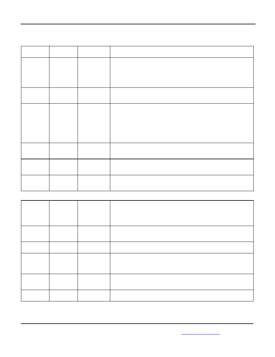
Pin Configuration
28-Pin SOIC (Z28-1)
32-Pin EPAD-TQFP (H32-1)
Micrel, Inc.
SY87700AL
November 2006
3
M9999-111406-B
hbwhelp@micrel.com
or (408) 955-1690
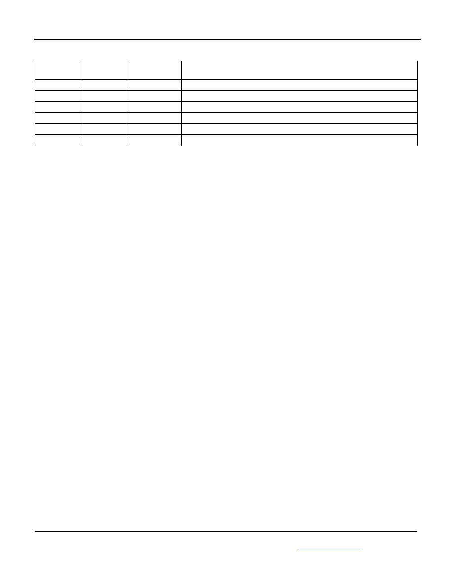
Pin Description
Inputs
Pin Number
(28-SOIC)
Pin Number
(32-TQFP)
Pin Name
Pin Name
4,
5
2,
3
RDINP,
RDINN
Serial Data Input. Differential PECL: These built-in line receiver inputs are
connected to the differential receive serial data stream. An internal receive
PLL recovers the embedded clock (RCLK) and data (RDOUT) information.
The incoming data rate can be within one of eight frequency ranges
depending on the state of the FREQSEL pins. See "Frequency Selection"
Table.
7 5
REFCLK
Reference Clock. TTL Input: This input is used as the reference for the
internal frequency synthesizer and the "training" frequency for the receiver
PLL to keep it centered in the absence of data coming in on the RDIN inputs
27 26 CD
Carrier Detect. PECL Input: This input controls the recovery function of the
Receive PLL and can be driven by the carrier detect output of optical
modules or from external transition detection circuitry. When this input is
HIGH the input data stream (RDIN) is recovered normally by the Receive
PLL. When this input is LOW the data on the inputs RDIN will be internally
forced to a constant LOW, the data outputs RDOUT will remain LOW, the
Link Fault Indicator output LFIN forced LOW and the clock recovery PLL
forced to lock onto the clock frequency generated from REFCLK.
6
8
9
4
6
7
FREQSEL1
FREQSEL2
FREQSEL3
Frequency Select. TTL Inputs: These inputs select the output clock frequency
range as shown in the "Frequency Selection" Table.
3
26
32
25
DIVSEL1
DIVSEL2
Divider Select. TTL Inputs: These inputs select the ratio between the output
clock frequency (RCLK/TCLK) and the REFCLK input frequency as shown in
the "Reference Frequency Selection" Table.
17 16
CLKSEL
Clock Select. TTL Input: This input is used to select either the recovered
clock of the receiver PLL (CLKSEL = HIGH) or the clock of the frequency
synthesizer (CLKSEL = LOW) to the TCLK outputs.
Outputs
2 31 LFIN
Link Fault Indicator. TTL Output: This output indicates the status of the input
data stream RDIN. Active HIGH signal is indicating when the internal clock
recovery PLL has locked onto the incoming data stream. LFIN will go HIGH if
CD is HIGH and RDIN is within the frequency range of the Receive PLL
(1000ppm). LFIN is an asynchronous output.
25
24
24
23
RDOUTP
RDOUTN
Receive Data Output. Differential PECL: These ECL 100k outputs represent
the recovered data from the input data stream (RDIN). This recovered data is
specified against the rising edge of RCLK.
22, 21
21, 20
RCLKP,
RCLKN
Clock Output. Differential PECL: These ECL 100k outputs represent the
recovered clock used to sample the recovered data (RDOUT).
19, 18
18, 17
TCLKP,
TCLKN
Clock Output. Differential PECL: These ECL 100k outputs represent either
the recovered clock (CLKSEL = HIGH) used to sample the recovered data
(RDOUT) or the transmit clock of the frequency synthesizer (CLKSEL =
LOW).
11, 12
9, 10
PLLSP,
PLLSN
Clock Synthesis PLL Loop Filter: External loop filter pins for the clock
synthesis PLL.
16, 15
15, 14
PLLRP,
PLLRN
Clock Recovery PLL Loop Filter: External loop filter pins for the receiver PLL.
Micrel, Inc.
SY87700AL
November 2006
4
M9999-111406-B
hbwhelp@micrel.com
or (408) 955-1690
Power and Ground
Pin Number
(28-SOIC)
Pin Number
(32-TQFP)
Pin Name
Pin Name
28 27,
28 VCC
Supply
Voltage
(1)
1
29, 30
VCCA
Analog Supply Voltage
(1)
20, 23
19, 22
VCCO
Output Supply Voltage
(1)
13, 14
12, 13
GND
Ground.
10
1, 8
NC
No connect.
11
GNDA
Analog
Ground.
Note:
1. VCC, VCCA, VCCO must be the same value.
Micrel, Inc.
SY87700AL
November 2006
5
M9999-111406-B
hbwhelp@micrel.com
or (408) 955-1690
Absolute Maximum Ratings
(1)
Supply Voltage (V
CC
) ................................... -0.5V to +4.0V
Input Voltage (V
IN
) ...........................................-0.5V to V
CC
Output Current (I
OUT
)
Continuous........................................................ ±50mA
Surge ..............................................................±100mA
Lead Temperature (soldering, 20sec.) ................... +260∞C
Storage Temperature (T
s
) ........................-65∞C to +150∞C
Operating Ratings
(2)
Input Voltage (V
CC
)............................. -3.15V to +3.45V
Ambient Temperature (T
A
) ................... ≠40∞C to +85∞C
Junction Thermal Resistance
(3)
SOIC
(
JA
)
(4)
.............................................. 27.3∞C/W
EPAD-SOIC
(
JA
)
(5)
....................................... 80∞C/W
EPAD-TQFP
(
JA
)
(5)
0lfpm
airflow........................................ 27.6∞C/W
200lfpm
airflow.................................... 22.6∞C/W
500lfpm
airflow.................................... 20.7∞C/W
DC Electrical Characteristics
Symbol Parameter
Condition
Min
Typ
Max Units
V
CC
Power
Supply
Voltage
3.15 3.3 3.45 V
I
CC
Power
Supply
Current
120 160 mA
PECL 100K DC Electrical Characteristics
V
CC
= V
CCO
= V
CCA
= 3.3V ±5%; T
A
= ≠40∞C to +85∞C, unless otherwise noted.
Symbol Parameter
Condition
Min
Typ
Max Units
V
IH
Input HIGH Voltage
V
CC
-1.165 V
CC
-0.880 V
V
IL
Input LOW Voltage
V
CC
-1.810
V
CC
-1.475 V
V
OH
Output HIGH Voltage
50 to V
CC
-2V V
CC
-1.075 V
CC
-0.830 V
V
OL
Output LOW Voltage
50 to V
CC
-2V V
CC
-1.860 V
CC
-1.570 V
I
IL
Input LOW Current
V
IN
= V
IL
(Min)
0.5
µA
TTL DC Electrical Characteristics
V
CC
= V
CCO
= V
CCA
= 3.3V ±5%; T
A
= ≠40∞C to +85∞C, unless otherwise noted.
Symbol Parameter
Condition
Min
Typ
Max Units
V
IH
Input HIGH Voltage
2.0
V
CC
V
V
IL
Input LOW Voltage
0.8
V
V
OH
Output HIGH Voltage
I
OH
= -0.4mA
2.0
V
V
OL
Output LOW Voltage
I
OL
= 4mA
0.5
V
I
IH
Input HIGH Current
V
IN
= 2.7V, V
CC
= Max.
V
IN
= V
CC
, V
CC
= Max.
-175
+100
µA
µA
I
IL
Input LOW Current
V
IN
= 0.5V, V
CC
= Max.
-300
µA
I
OS
Output Short-Circuit Current
V
OUT
= 0V, (Max., 1 sec.)
-15
-100
mA
Notes:
1. Permanent device damage may occur if absolute maximum ratings are exceeded. This is a stress rating only and functional operation is not
implied at conditions other than those detailed in the operational sections of this data sheet. Exposure to absolute maximum rating conditions for
extended periods may affect device reliability.
2. The data sheet limits are not guaranteed if the device is operated beyond the operating ratings.
3. Airflow of 500lfpm recommended for 28-pin SOIC.
4. 28-pin SOIC package is NOT recommended for new designs.
5. Using JEDEC standard test boards with die attach pad soldered to PCB. See www.amkor.com for additional package details.