 | –≠–ª–µ–∫—Ç—Ä–æ–Ω–Ω—ã–π –∫–æ–º–ø–æ–Ω–µ–Ω—Ç: SY87724L | –°–∫–∞—á–∞—Ç—å:  PDF PDF  ZIP ZIP |
DESCRIPTION
FEATURES
SY87724L
FINAL
s
Protocol transparent mux/demux operation up to
2.7GHz
s
Programmable to 4, 5, 8, or 10 bit parallel interfaces
s
Differential clock and serial inputs/outputs
s
Easily controlled by framer logic
s
Synchronous frame boundary indication
s
HSPC (High Speed PECL Compatible) inputs and
outputs
s
3.3V power supply
s
Available in 80-pin LQFP-PQ2 package
The SY87724L is a complete serial data multiplexer and
demultiplexer, capable of operating at up to 2.7GHz. The
device provides for muxing and demuxing to 4, 5, 8, or 10
bit wide buses.
The SY87724L can accept a synchronous code group or
octet boundary input, and uses this input for parallel data
alignment.
The SY87724L is manufactured in Micrel's high
performance ASSET2TM silicon bipolar process.
Micrel provides a complete protocol transparent solution
with the AnyRateTM SY87721L CDR/CMU SY87729L, and
the SY87724L integrated mux/demux.
3.3V AnyRateTM
MUX/DEMUX
Up to 2.7GHz
APPLICATIONS
s
OC-3, OC-12, OC-48, ATM, InfiniBand
s
Gigabit Ethernet
s
Fibre Channel, 2X Fibre Channel
s
SMPTE-259 and 292
s
Proprietary optical transport
s
ITU G. 975 Solutions
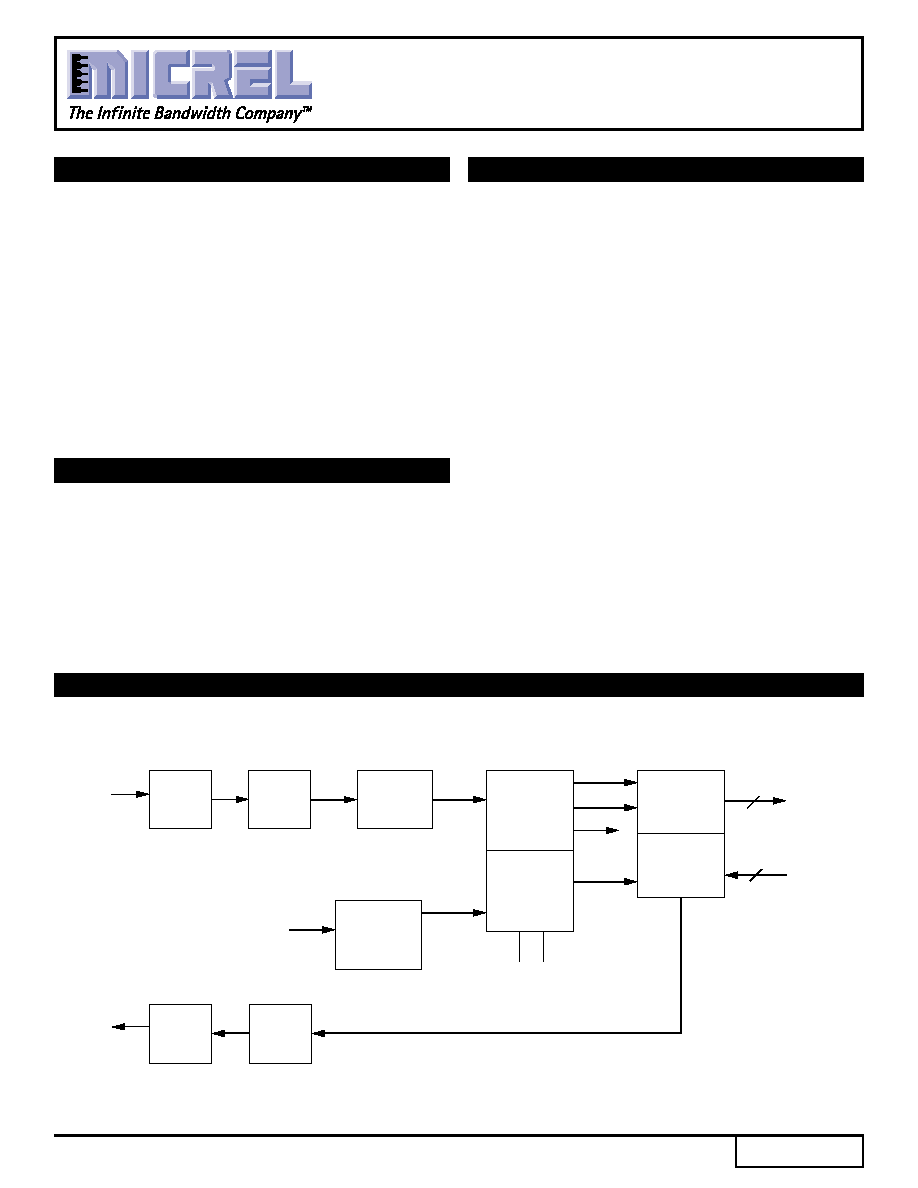
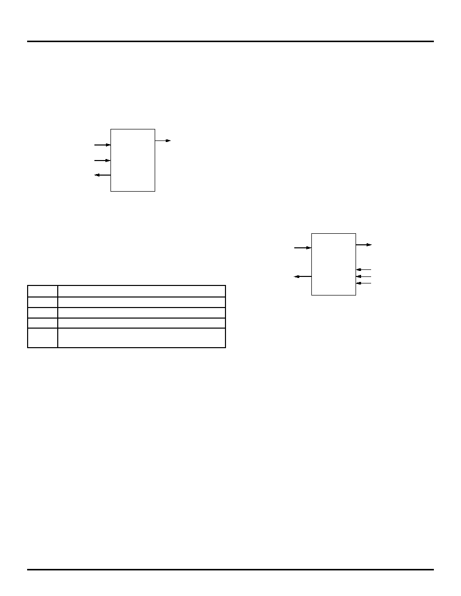
SYSTEM BLOCK DIAGRAM
1
Rev.: A
Amendment: /0
Issue Date:
September 2001
AnyRate is a trademark of Micrel, Inc.
DEMUX
TCLK
4, 5, 8, 10 bits
4, 5, 8, 10 bits
LOCK
RCLK
RDATA
SY87724L
POST AMP
TIA
PIN DIODE
FIBER
LASER
DIODE
FIBER
SY889x3
CMU
CDR
SY87721L
AnyRateTM
REF_CLK
SEL
One
REF_XTAL
SY87729L
SY889x2
AnyClockTM
LASER
DIODE
DRIVER
Fractional
Synthesizer
CD
MUX
SY87724L
FINAL
2
Micrel
FUNCTIONAL BLOCK DIAGRAM
DSIN
±
MSOUT
±
(From Mux)
Mux
DCKIN
±
DFMIN
±
Mux
Parallel In
Parallel Out
Register
(5 bits)
5
Serial In
Parallel Out
Shift
Register
(5 bits)
Mux
MTKCLK
±
(From Mux)
SIZ0
SIZ1
SIZ2
LPBK
Demux
Internal Control
Demux
Strobe Generator
Parallel In
Parallel Out
Register
(5 bits)
5
5
Parallel In
Parallel Out
Register
(5 bits)
Parallel In
Parallel Out
Register
(5 bits)
Parallel In
Parallel Out
Register
(5 bits)
5
5
5
DP0≠4
±
DP5≠9
DPOUTCK
±
Dela
y
Primary Divider
(
˜
4 or
˜
5)
MSYNOUT
±
(From Mux)
Demux
SY87724L
FINAL
3
Micrel
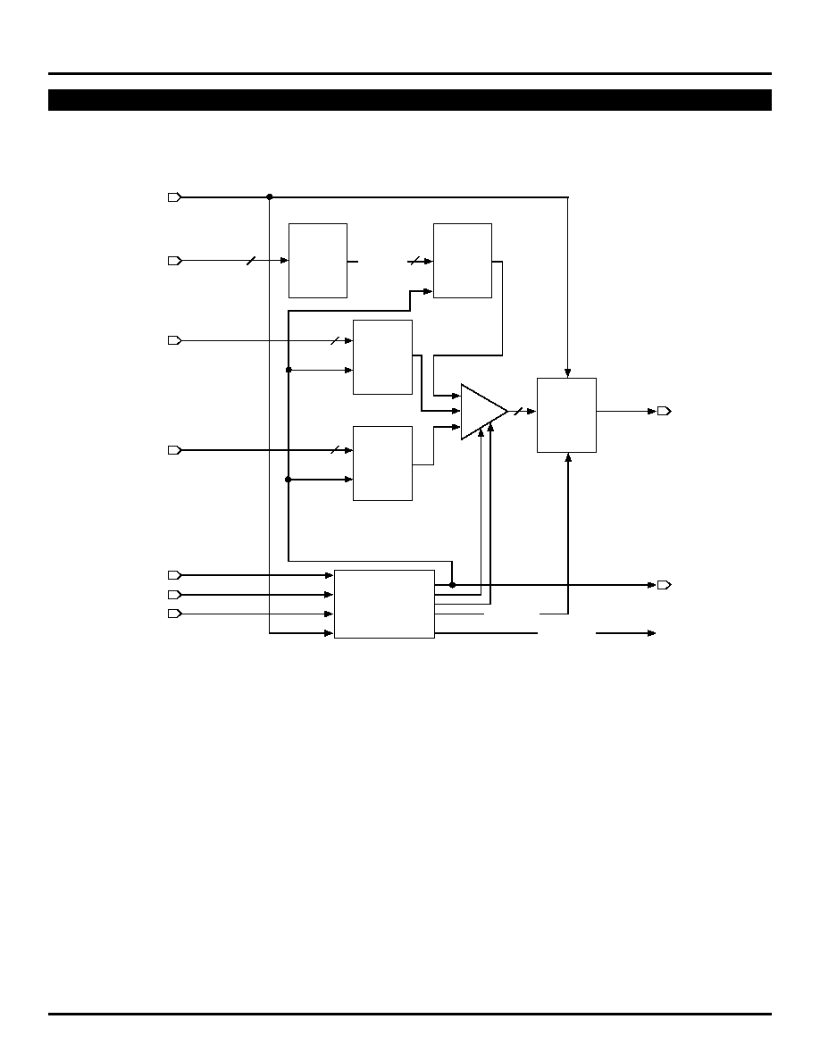
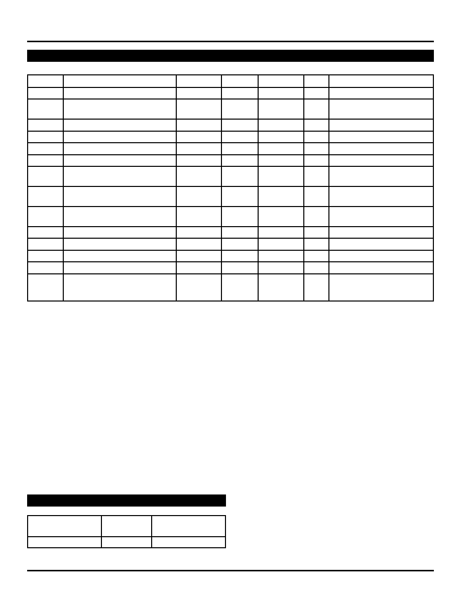
FUNCTIONAL BLOCK DIAGRAM
Mux
MTXCLK
±
Parallel In
Parallel Out
Register
(5 bits)
Parallel In
Parallel Out
Register
(5 bits)
Parallel In
Parallel Out
Register
(5 bits)
Mux
5
5
5
5
MP0≠4
MP5≠9
MPF0≠4
±
Mux Strobe
Generator
Load/Shift
SIZ0
SIZ1
SIZ2
Serial and
Parallel In
Serial Out
Shift
Register
(5 bits)
MSOUT
±
MPINCK
±
Parallel In
Parallel Out
MP0≠4
±
MSYNOUT
±
(to Demux)
5
SY87724L
FINAL
4
Micrel
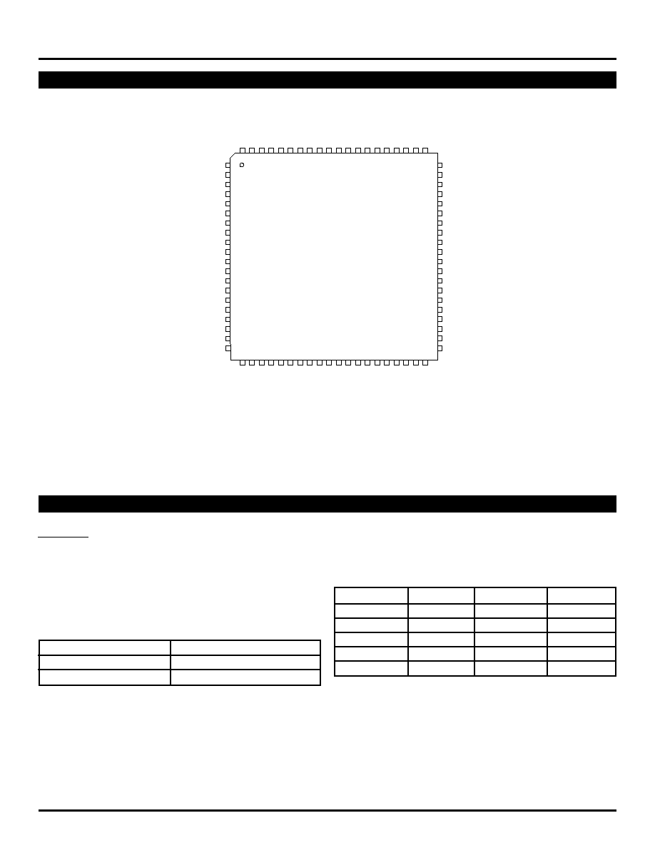
PIN CONFIGURATION
1
80-PIN
LQFP-PQ2
2
3
4
5
6
7
8
9
10
11
12
13
21 22 23 24 25 26 27 28 29 30 31 32 33
60
59
58
57
56
55
54
53
52
51
50
49
48
77 76 75 74 73 72 71 70 69 68 67 66 65
GND
VCC
NC
NC
SIZ1
SIZ2
MP1
MP2
MP3
MP4
NC
14
15
16
47
46
45
78
79
80
34 35 36
MTXCLK+
SIZ0
MP0
MP5
MP6
MP7
NC
VCCO
17
18
19
20
37 38 39 40
44
43
42
41
64 63 62 61
MP8
MP9
VCC
VCCO
NC
GND
MSOUT+
MSOUT
≠
LPBK
VCC
NC
NC
MPINCK+
MPINCK
≠
VCCO
DFMIN+
DFMIN
≠
DSIN+
DSIN
≠
GND
VCC
VCC
GND
DCKIN+
DCKIN≠
VCCO
DP9
DP8
DP7
DP6
DP5
DP4≠
DP4+
DP3≠
DP3+
VCCO
VCCO
DP2≠
DP2+
DP1≠
DP1+
VCC
MTXCLK
≠
GND
MPF0+
MPF0
≠
MPF1+
MPF1
≠
MPF2+
MPF2
≠
MPF3
≠
MPF3+
MPF4+
MPF4
≠
VCC
GND
VCCO
DPOUTCK+
DPOUTCK
≠
DP0+
DP0
≠
PIN NAMES
COMMON
LPBK ≠ TTL Input
This pin defines whether a device exhibits local loopback
or not, as per the following table. Loopback internally
connects mux serial out to demux serial in, thus the user
may expect mux side parallel data to appear on the demux
parallel output pins.
LPBK
Functioning
0
Loopback
1
Normal
SIZ0, SIZ1, SIZ2 ≠ TTL Input
These three signals determine the width of the parallel
output, as well as the width of parallel input. The following
table describes the parallel width options.
Width
SIZ0
SIZ1
SIZ2
(1)
4
0
0
0
5
1
0
0
8
0
1
0
10
1
1
0
Undefined
X
X
1
Note:
1. Pin 8 (SIZ2) should always be tied to a TTL logic level LOW.

SY87724L
FINAL
5
Micrel
DEMUX
DSIN
±
≠ Differential HSPC Input
This is the serial input to the SY87724L demux. It accepts
the serial data and converts it to parallel data. It is ignored
during loopback.
DCKIN
±
≠ Differential HSPC Input
This is the bit rate clock that feeds serial data into the
demux shift register. This signal also feeds the demux strobe
generator and primary divider, except during loopback.
DFMIN
±
≠ Differential HSPC Input
This is the frame alignment input signal. This signal resets
the primary divider, as well as the strobe generator. This
effectively sets the alignment for the parallel data being
demuxed. Usually, DFMIN
±
asserts one DCKIN
±
before a
parallel word boundary, and continues to assert one clock
before every boundary. However, DFMIN
±
need only occur
once for proper operation. Should DFMIN
±
assert at other
than a previously set boundary, the DPOUTCK
±
signal will
always occur later than would be expected. That is, there
will never be a short DPOUTCK
±
pulse.
DP0
±
through DP4
±
≠ Differential PECL Output
These signals may be used as either differential, or single-
ended. When converting to 4 or 5 bits, speed issues may
encourage the use of these signals differentially. When
converting to wider than 5 bits, these signals are to be used
single-ended. Please refer to the applications section for
further details.
DP5 through DP9 ≠ PECL Output
These are the rest of the parallel output bits, to be used
when converting to wider than 5 bits. Which bits are valid
depends on the values of SIZ0, SIZ1, and SIZ2. Please
refer to the table in the applications section for further details.
DPOUTCK
±
≠ Differential HSPC Output
This signal is used to strobe the DP0-9 data. It is used
differentially when converting to 4 or 5 bits, and is used
single-ended when converting to wider than 5 bits. The
clock rate of the line will be determined by the DCKIN
signal, and by the setting of the SIZ bits. This output always
provides valid differential logic levels.
MUX
MP0-9 ≠ PECL Input
These bits accept data for muxing wider than 5 bits.
MPINCK+, used single-ended, determines when this data
may change. Please refer to the table in the description for
which pins represent what bits for various widths.
MPF0≠4
±
≠ Differential PECL Input
These signals are used when muxing 4 or 5 bits of parallel
data. MPINCK
±
determines when this data may change.
Please refer to the Mux table in the description for which
pins represent what bits for various widths.
MTXCLK
±
≠ Differential HSPC Input
This is the serial rate clock input to the mux. It determines
the rate at which serial data will be shifted out of the mux.
MSOUT
±
≠ Differential PECL Output
This signal is the serialized data output.
MPINCK
±
≠ Differential PECL Output
This signal indicates when the next set of parallel bits
may be presented to the SY87724L for muxing. For muxing
wider than 5 bits, MPINCK+ is used single-ended. These
signals always provide valid differential clock signals
regardless of single-ended or differential data mode.
OTHER
V
CC
Supply Voltage
V
CCO
Output Supply Voltage
GND
Ground
NC
These pins are reserved and are to be left
unconnected.
Note:
1. All differential outputs always provide valid differential logic levels regardless
of differential or single-ended use.

SY87724L
FINAL
6
Micrel
DESCRIPTION
General
The SY87724L MDM is designed to perform muxing and
demuxing at up to 2.7GHz speeds. The device can
simultaneously mux and demux up to 10 bits of full duplex
data. In addition, a full parallel-to-parallel loopback function
is implemented, such that parallel data out will loop back to
parallel data in, with the device internally connecting the
serial output to the serial input.
Narrow Demux
In this example, serial data is converted into 4 or 5 bit
wide data. Because this can result in very high data rates
on the parallel outputs, they are differential. The DFMIN
±
input indicates, synchronously with DCKIN
±
, and one clock
ahead, the start of a 4 or 5 bit boundary.
MDM
DP0-4
±
DPOUTCK
±
DSIN
±
DCKIN
±
DFMIN
±
Figure 1. Narrow Demux
Every DFMIN
±
assertion will trigger a new 4 or 5 bit
boundary. Should only one DFMIN
±
assertion occur, then
DPOUTCK
±
will continue to assert every 4 or 5 DCKIN
±
clocks. Should a subsequent DFMIN
±
assertion reset the 4
or 5 bit boundary, then DPOUTCK
±
will always result in a
longer assertion, not a shorter one.
For example, if a subsequent DFMIN
±
resets a 5 bit
boundary after the second bit in relation to a previous
boundary, then the next DPOUTCK
±
will always occur 7
DCKIN
±
later, never 2 DCKIN
±
later. For four bit output,
DP5
±
are not used.
Wide Demux
The more typical case will be to convert the serial data
stream into 8 or 10 bit wide data. Because the worst case
parallel transfer rate is on the order of 250 to 340 Mega-
transfers per second, single ended parallel output is
preferred. Thus, only the single-ended side of the differential
outputs is used.
This example is much like the narrow demux, except
now DFMIN
±
indicates 8 or 10 bit boundaries.
MDM
DP0-4+
DPOUTCK+
DSIN
±
DCKIN
±
DFMIN
±
DP5-9
Figure 2. Wide Demux
As in the narrow case, DPOUTCK
±
will never assert
twice in 8 or 10 DCKIN
±
cycles. Should a DFMIN
±
assertion
change the MDM's 8 or 10 bit boundary, DPOUTCK
±
assertion will be delayed and there will never be a short
assertion.
For 8 bit output, DP4
±
and DP9 are not used.
The following table summarizes the available bit widths.
The right column shows the parallel bits, in sequence from
first in serially, to last in.
Width
Sequence
4
DP0
±
, DP1
±
, DP2
±
, DP3
±
5
DP0
±
, DP1
±
, DP2
±
, DP3
±
, DP4
±
8
DP0+, DP1+, DP2+, DP3+, DP5, DP6, DP7, DP8
10
DP0+, DP1+, DP2+, DP3+, DP4+, DP5, DP6, DP7,
DP8, DP9
Narrow Mux
In this scenario, 4 or 5 bit wide parallel data is converted
to a serial bit stream. Because this can result in very high
data rates on the parallel inputs, they are differential. In this
mode of operation, there is no external synchronization,
and the MPINCK
±
signal pair has arbitrary phase with
respect to the MTXCLK
±
clock, which clocks the mux output
shift register.
MDM
MSOUT
±
MPF0-4
±
MPINCK
±
MTXCLK
±
Figure 4. Narrow Mux
MPINCK
±
indicates when MDM is ready to accept more
data. It is derived from MTXCLK
±
, with an arbitrary phase
relationship.
SY87724L
FINAL
7
Micrel
Wide Mux
The more typical case will be to convert 8 or 10 bit wide
parallel data words into a serial bit stream. Because the
worst case parallel input rate is on the order of 250 to 340
Mega-transfers per second, single ended parallel inputs are
used.
This scenario is much like the narrow mux case, except
now MPINCK+ clocks slower, for 8 or 10 bit parallel words.
MDM
MSOUT
±
MP0-9
MPINCK+
MTXCLK
±
Figure 5. Wide Mux
Note that the input data indication is now single ended,
and that completely different input pins are used, as
compared to the 4 or 5 bit case.
The following table summarizes the available bit widths.
The right column shows the parallel input bits, such as they
will appear in the serial output stream.
Width
Sequence
4
MPF0
±
, MPF1
±
, MPF2
±
, MPF3
±
5
MPF0
±
, MPF1
±
, MPF2
±
, MPF3
±
, MPF4
±
8
MP5, MP6, MP7, MP8, MP0, MP1, MP2, MP3
10
MP5, MP6, MP7, MP8, MP9, MP0, MP1, MP2, MP3,
MP4
Loopback
To ease system design, the SY87724L MDM has the
capability to loop parallel data in, through the mux, into the
demux, and back to parallel data out. This permits system
check-out through to the individual MDM device. Note that,
for a full check-out, some form of loopback further down the
serial stream is required.
Loopback is incorporated into MDM by modifying the
serial clock, data, and sync inputs to the demux stage.
During loopback, the source of serial information for the
demux is changed. The MSOUT
±
,
MTXCLK
±
and
MSYNOUT
±
are internally muxed to the DSIN
±
, DCKIN
±
,
and DFMIN
±
nodes of the demux section. The MSYNOUT
±
signal
has
the same characteristics as the DFMIN logic
expects.
This exercises the internal data path, both mux and
demux, for MDM, and also the control logic. The parallel
data presented to the parallel inputs will appear, some small
but unspecified time later, at the parallel outputs.
MSOUT
±
DFMIN
±
MP*
DP*
* Number of wires depends on the SIZX bits.
DCKIN
±
DSIN
±
SY87724L
FINAL
8
Micrel
Symbol
Parameter
Rating
Unit
V
CC
Power Supply Voltage
≠0.5 to +3.8
V
V
I
Input Voltage
≠0.5 to V
CC
(2)
V
I
OUT
ECL Output Current
--Continuous
50
mA
--Surge
100
T
store
Storage Temperature Range
≠65 to +150
∞
C
T
A
Operating Temperature Range
≠40 to +85
∞
C
NOTES:
1. Permanent device damage may occur if ABSOLUTE MAXIMUM RATINGS are exceeded. This is a stress rating only and functional operation is not implied
at conditions other than those detailed in the operational sections of this data sheet. Exposure to ABSOLUTE MAXIMUM RATING conditions for extended
periods may affect device reliability.
2. The maximum value is specified at V
CC
up to V
CC
= +6V.
ABSOLUTE MAXIMUM RATINGS
(1)
Symbol
Parameter
Min.
Typ.
Max.
Unit
Condition
V
CC
Power Supply Voltage
3.15
3.3
3.45
V
I
CC
Power Supply Current
--
650
750
mA
V
CC
= V
CCA
= 3.15V to 3.45V
DC ELECTRICAL CHARACTERISTICS
(1)
Symbol
Parameter
Min.
Typ.
Max.
Unit
Condition
V
IN
Input HIGH Voltage
V
CC
≠ 1.810
--
V
CC
V
V
ID
Input Voltage
0.2
--
--
V
Differential Swing
(2)
I
IL
Input LOW Current
≠0.5
--
--
µ
A
V
IN
= V
IL
(Min)
V
OH
Output HIGH Voltage
V
CC
≠ 1.0
--
V
CC
≠ 0.75
V
50
to V
CC
≠2V
V
OL
Output LOW Voltage
V
CC
≠ 1.55
--
V
CC
≠ 1.25
V
50
to V
CC
≠2V
V
OSW
Output Voltage
0.3
--
--
V
Differential Swing
V
CC
= V
CCA
= 3.15V to 3.45V
HSPC DC ELECTRICAL CHARACTERISTICS
(1)
NOTE:
1. Operating temperature range from ≠40
∞
C to +85
∞
C.
NOTE:
1. Operating temperature range from ≠40
∞
C to +85
∞
C.
2. This implies that the common mode range, V
CMR
, goes from V
IN
(min) + V
ID
/2 through V
IN
(max) - V
ID
/2.

SY87724L
FINAL
9
Micrel
Symbol
Parameter
Min.
Typ.
Max.
Unit
Condition
V
IH
Input HIGH Voltage
V
CC
≠ 1.165
--
V
CC
≠ 0.880
V
V
IL
Input LOW Voltage
V
CC
≠ 1.810
--
V
CC
≠ 1.475
V
I
IL
Input LOW Current
≠0.5
--
--
µ
A
V
IN
= V
IL
(Min)
V
OH
Output HIGH Voltage
V
CC
≠ 1.075
--
V
CC
≠ 0.830
V
50
to V
CC
≠2V
V
OL
Output LOW Voltage
V
CC
≠ 1.860
--
V
CC
≠ 1.570
V
50
to V
CC
≠2V
V
OSW
Output Voltage
0.6
--
--
V
Differential Swing
V
CC
= V
CCA
= 3.15V to 3.45V
PECL DC ELECTRICAL CHARACTERISTICS
(1)
Symbol
Parameter
Min.
Typ.
Max.
Unit
Condition
V
IH
Input HIGH Voltage
2.0
--
--
V
V
IL
Input LOW Voltage
--
--
0.8
V
I
IH
Input HIGH Current
--
--
+20
µ
A
V
IN
= 2.7V, V
CC
= Max.
--
--
+100
µ
A
V
IN
= V
CC
, V
CC
= Max.
I
IL
Input LOW Current
--
--
300
µ
A
V
IN
= 0.5V, V
CC
= Max.
V
CC
= V
CCA
= 3.15V to 3.45V
TTL DC ELECTRICAL CHARACTERISTICS
(1)
NOTE:
1. Operating temperature range from ≠40
∞
C to +85
∞
C.
NOTE:
1. Operating temperature range from ≠40
∞
C to +85
∞
C.
SY87724L
FINAL
10
Micrel
Symbol
Parameter
Min.
Typ.
Max.
Unit
Condition
f
MAX
Maximum Operating Frequency
2.7
--
--
GHz
t
DCKPWH
,
Demux Clock Pulse Duty Cycle
45
--
55
%
t
DCKPWH
t
DSDS
Demux Serial Data Setup
200
--
--
ps
t
DSDH
Demux Serial Data Hold
0
--
--
ps
t
DSFS
Demux Serial Frame Setup
150
--
--
ps
t
DSFH
Demux Serial Frame Hold
50
--
--
ps
t
DPDP
Demux Parallel
+200
--
+800
ps
Differential Propagation
t
DPSP
Demux Parallel
+200
--
+1200
ps
Single-Ended Propagation
t
MCKPWH
,
Mux Clock Pulse Duty Cycle
45
--
55
%
t
MCKPWL
t
MPDS
Mux Parallel Differential Setup
(2)
T
cyc
+650
--
--
ps
t
MPDH
Mux Parallel Differential Hold
(2)
≠(T
cyc
+250)
--
--
ps
t
MPSS
Mux Parallel Single-Ended Setup
(2)
T
cyc
+850
--
--
ps
t
MPSH
Mux Parallel Single-Ended Hold
(2)
≠(T
cyc
+50)
--
--
ps
t
r
, t
f
Output Rise/Fall Times
50
to V
CC
≠ 2V
MCKOUT, MSOUT, MSYNOUT
--
100
120
ps
(20% to 80%)
All Others
--
--
500
V
CC
= V
CCA
= 3.15V to 3.45V
AC ELECTRICAL CHARACTERISTICS
NOTES:
1. Operating temperature range from ≠40
∞
C to +85
∞
C.
2. T
cyc
= the period of the clock being fed into MTXCLK.
PRODUCT ORDERING CODE
Ordering
Package
Operating
Code
Type
Range
SY87724LH1
H80-1
Industrial
SY87724L
FINAL
11
Micrel
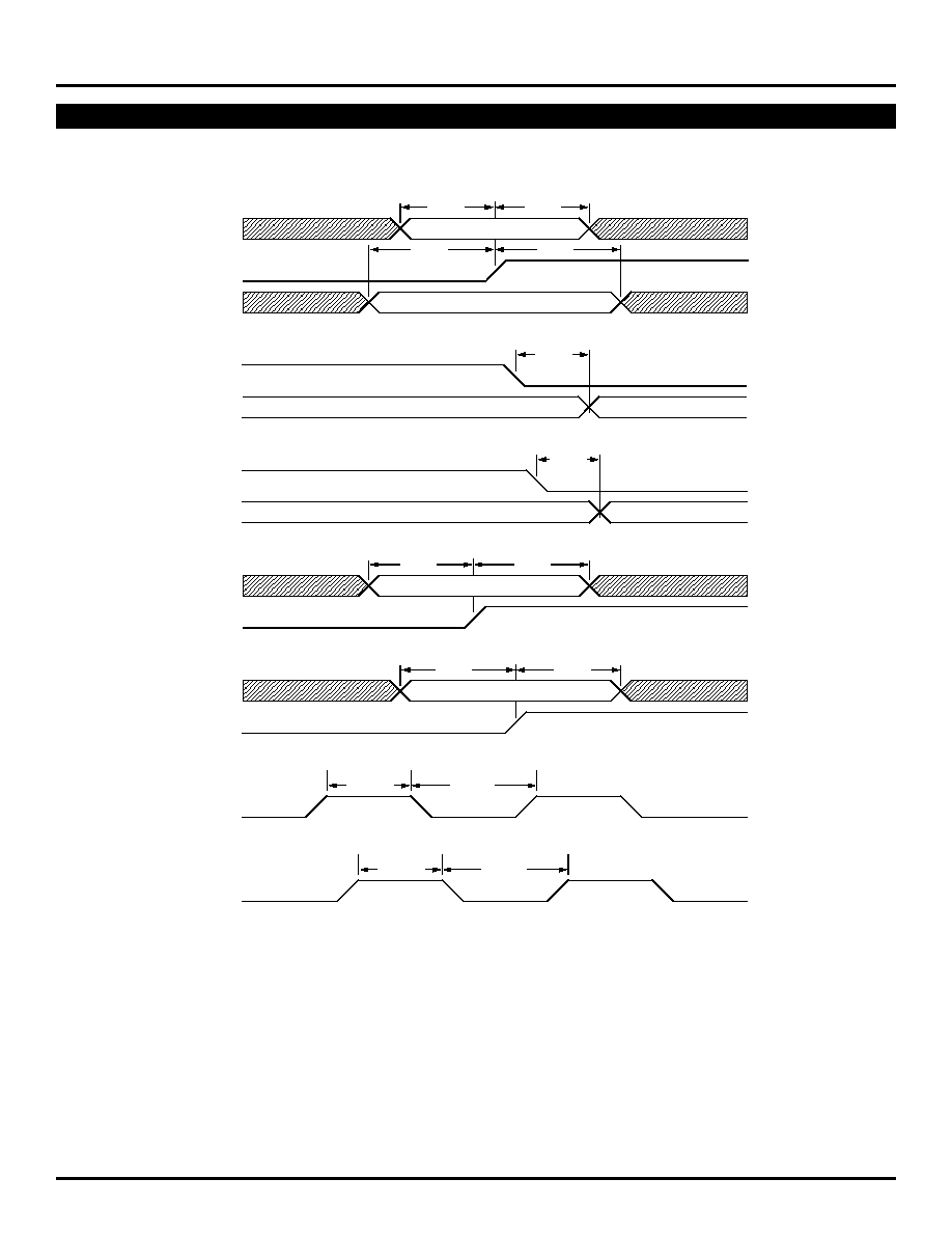
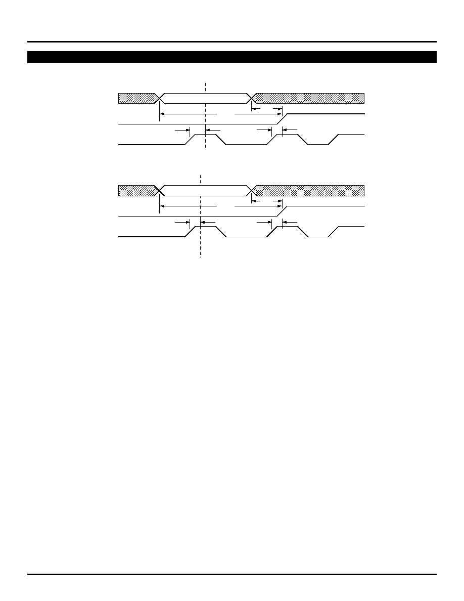
TIMING WAVEFORMS
t
DSFS
t
DSFH
t
DSDS
t
DSDH
DSIN
±
DCKIN
±
DFMIN
±
t
DPDP
DPOUTCK
±
DP0≠4
±
t
DPSP
DPOUTCK+
DP0≠4+
DP5≠9
t
MPDS
t
MPDH
MPF0≠4
±
MPINCK
±
t
MPSS
t
MPSH
MP0≠9
MPINCK+
t
DCKPWH
t
DCKPWL
DCKIN
±
t
MCKPWH
t
MCKPWL
MTXCLK
±
Valid
Valid
Valid
Valid
SY87724L
FINAL
12
Micrel
TIMING APPLICATION EXAMPLE
1750
1350
MPF0-4
±
MPINCK
±
Valid
x
y
MTXCLK
±
1950
1150
MPF0-9
±
MPINCK
±
Valid
x
y
MTXCLK
±
NOTES:
1. MTXCLK = 1Gbps
2. Time "
x
" is approximately equal to time "
y
."
3. Setup and hold for MPF0-4
±
is conditioned on the MTXCLK
±
rising edge
just prior to the MTXCLK
±
rising edge that causes an MPINCK
±
rising
edge.
SY87724L
FINAL
13
Micrel
MICREL-SYNERGY
3250 SCOTT BOULEVARD
SANTA CLARA
CA 95054
USA
TEL
+ 1 (408) 980-9191
FAX
+ 1 (408) 914-7878
WEB
http://www.micrel.com
This information is believed to be accurate and reliable, however no responsibility is assumed by Micrel for its use nor for any infringement of patents or
other rights of third parties resulting from its use. No license is granted by implication or otherwise under any patent or patent right of Micrel Inc.
© 2001 Micrel Incorporated
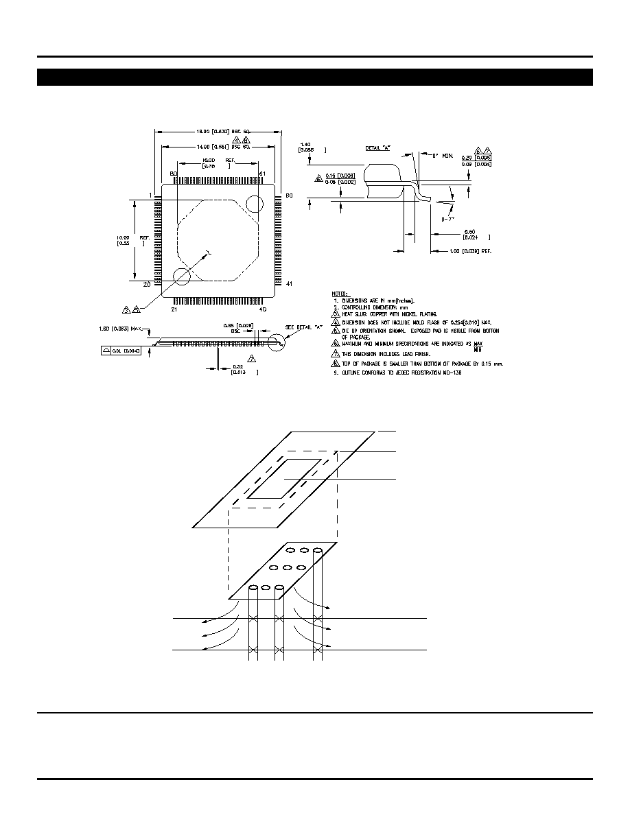
80 LEAD LQFP-PQ2 (DIE UP) (H80-1)
Rev. 00
+0.06
≠0.10
+0.002
≠0.004
+0.006
≠0.006
+0.15
≠0.15
+0.05
≠0.05
+0.002
≠0.002
+0.020
≠0.020
+0.5
≠0.5
+0.020
≠0.020
+0.5
≠0.5
Package
EP- Exposed Pad
Die
CompSide Island
Heat Dissipation
Heavy Copper Plane
Heavy Copper Plane
V
EE
V
EE
Heat Dissipation
PCB Thermal Consideration for 80-Pin EPAD-TQFP Package