DESCRIPTION
s
Protocol transparent fractional-N synthesizer from
10MHz to 729MHz from a single 27MHz reference
oscillator
s
Generates exactly the correct frequency for common
transport protocols with or without FEC
s
Directly enables SY87721L CDR to lock onto any
data rate within its range
s
Exceeds BellCore and ITU jitter generation
specifications
s
Programmable via MicroWireTM interface
s
Available in 32-Pin EPAD-TQFP package
FEATURES
PROTOCOL TRANSPARENT
3.3V 10MHz to 729MHz
FRACTIONAL-N SYNTHESIZER
SY87739L
Final
APPLICATIONS
s
Metro access system
s
Transponders
s
Multiplexers: access, Add Drop Mux
s
SONET/SDH/ATM-based transmission systems,
modules and test equipment
s
Broadband cross-connects
s
Fiber optic test equipment
s
Protocols supported:
OC-1, OC-3, OC-12, OC-48, ATM, Gigabit Ethernet,
Fast Ethernet, Fibre Channel, 2X Fibre Channel,
1394, InfiniBand, Proprietary Optical Transport
1
Rev.: A
Amendment: /0
Issue Date:
October 2002
The SY87739L is a complete rate independent frequency
synthesizer integrated circuit. From a single reference
source, this device generates a differential PECL output
frequency from 10MHz up to 729MHz.
The SY87739L generates an exactly correct reference
frequency for common data transport protocols. This is
especially important in transponder applications, where a
standards compliant protocol data unit must be generated
downstream, even in the absence of any signal from the
associated upstream interface. In addition, the SY87739L
will generate exactly correct reference frequencies for
common data transport protocols augmented by forward
error correction codes. The SY87739L accepts configuration
via a MicroWireTM interface.
For proprietary applications, the SY87739L generates
reference frequencies guaranteed to enable the SY87721L
CDR to lock to any possible baud rate from 28Mbps to
2.7Gbps.
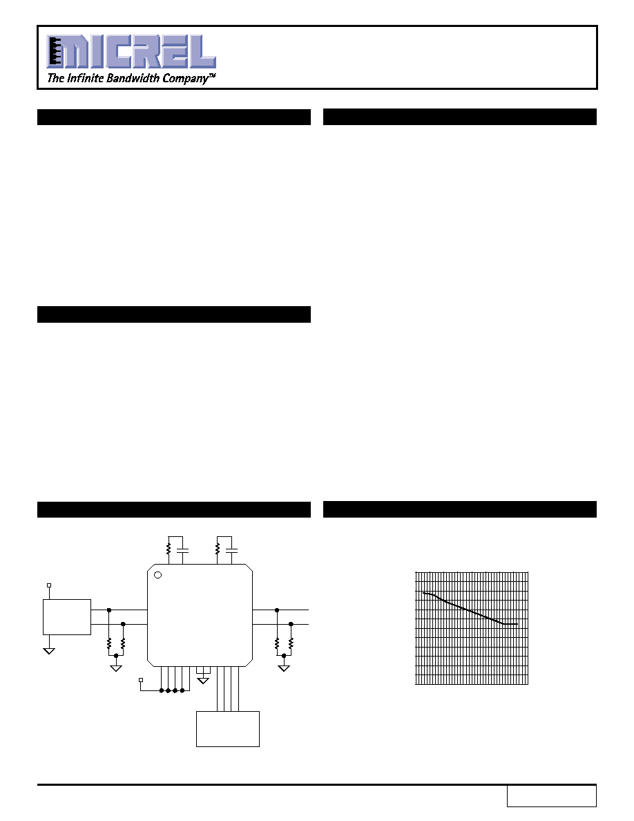
TYPICAL APPLICATIONS CIRCUIT
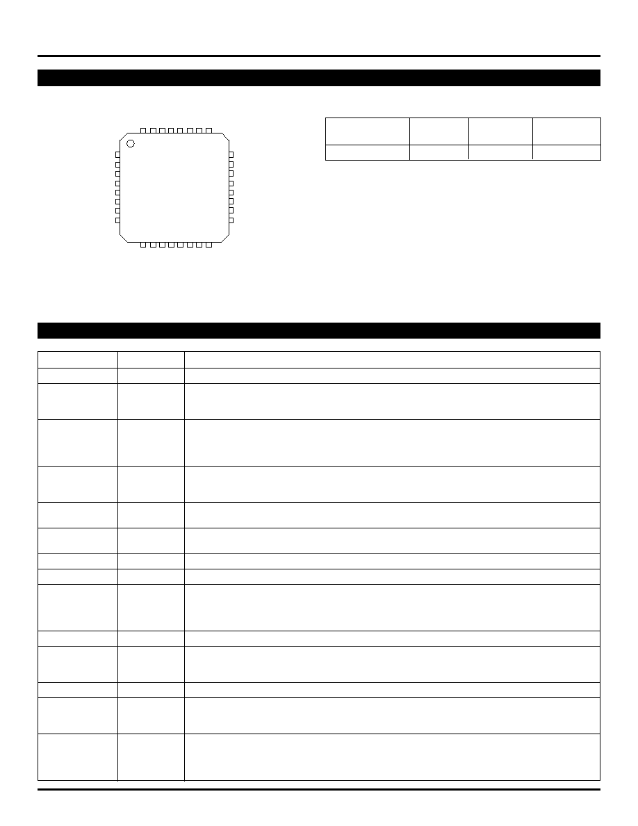
TYPICAL PERFORMANCE
AnyClock and AnyRate are trademarks of Micrel, Inc.
MicroWire is a trademark of National Semiconductor.
1, 9, 17, 18, 24
10, 25, 32
6
3
4
22
21
SY87739L
REFCLK+
REFCLK--
CLKOUT+
CLKOUT--
7 8 14
V
CC
OUT
OUT
OUT
IN
Microcontroller
PROGCS
PROGSK
PROGDI
LOCKED
31
30
26
25
2k
2k
0.1
µ
F
0.1
µ
F
121
121
121
121
FNVCF+
FNVCF
--
WR
VCF+
WR
VCF
--
Saronix
SEL-2431C
27.0000MHz
8
1
V
CC
7
14
0
1
2
3
4
5
6
0 100 200 300 400 500 600 700 800
RMS JITTER (ps)
OUTPUT FREQUENCY (MHz)
Cycle-to-Cycle Jitter
vs. Frequency
2
SY87739L
Micrel
PACKAGE/ORDERING INFORMATION
Ordering Information
Package
Operating
Package
Part Number
Type
Range
Marking
SY87739LHI
H32-2
Industrial
SY87739LHI
NC
NC
FNVCF
--
FNVCF+
GNDA
WR
VCF+
WR
VCF
--
GNDA
NC
NC
NC
GND
VCC
LOCKED
NC
NC
VCCA
NC
CLKOUT+
CLKOUT--
NC
NC
VCCO
VCC
VCCA
NC
REFCLK+
REFCLK--
NC
PROGCS
PROGDI
PROGSK
32 31 30 29 28 27 26 25
9 10 11 12 13 14 15 16
1
2
3
4
5
6
7
8
24
23
22
21
20
19
18
17
EPAD-TQFP (H32-2)
Pin Number
Pin Name
Pin Function
1, 24
VCCA
Analog Supply (Power). Set to same voltage as V
CC
.
2, 5, 11, 12, 13,
NC
No Connect. These pins are to be left unconnected.
15, 16, 19, 20
23, 28, 29
3, 4
REFCLK
±
Reference Clock Input (Differential PECL Input): This is a clock derived from an oscillator or
other sufficiently accurate frequency source. The frequency provided at this input determines,
along with the programming, the output frequency at REFOUT
±
. Micrel recommends using a
27.000MHz frequency source.
6
PROGCS
Program Interface Chip Select (TTL Input): This signal forms part of the MicroWireTM interface.
When active high, this signal permits the acquisition of serial data. A falling edge on this input
causes SY87739L to re-acquire lock to a new frequency, based on the program downloaded to it.
7
PROGDI
Program Interface Data In (TTL Input): One data bit is sampled on each rising edge of PRGSK,
while PROGCS is active high.
8
PROGSK
Program Interface Serial Clock (TTL Input): One bit of configuration data is read in each clock
cycle.
9, 17,
VCC
Supply (Power): +3.15V to +3.45V.
10
GND
Ground.
14
LOCKED
Lock Output (TTL Output): This indicates proper operation of all the blocks in the clock synthesis
chain. Logic high indicates that SY87739L is generating the expected frequency at the CLKOUT
±
output. Logic low indicates that one or more PLL in the clock synthesis chain has yet to achieve
proper lock.
18
VCCO
Output Supply (Power). Set to same voltage as V
CC
.
21, 22
CLKOUT
±
Reference Clock Output (Differential PECL Output): This is the synthesized clock generated from
REFCLK
±
. It can be used to supply a reference clock to a data recovery device, such as Micrel's
SY87721L.
25, 32
GNDA
Analog Ground.
26, 27
WRVCF
±
Wrapper Filter (Analog I/O): These pins connect to the output from the wrapper synthesizer
charge pump, as well as the input to the corresponding VCO. A filter network, as described
below, converts the charge pump current to a voltage, and adjusts loop bandwidth.
30, 31
FNVCF
±
Fractional-N Filter (Analog I/O): These pins connect to the output from the fractional-N synthesizer
charge pump, as well as the input to the corresponding Voltage Controlled Oscillator (VCO). A
filter network, as described below, converts the charge pump current to a voltage, and adjusts
loop bandwidth.
PIN DESCRIPTION
3
SY87739L
Micrel
Absolute Maximum Ratings
(Note 1)
Supply Voltage (V
CC
) .................................. ≠0.5V to +5.0V
Input Voltage(V
IN
) ...................................... ≠0.5V to V
CC
ECL Output Current (I
OUT
)
Continuous ......................................................... 50mA
Surge ................................................................ 100mA
Lead Temperature (soldering, 10 sec.) ..................... 220
∞
C
Storage Temperature (T
S
) ....................... ≠65
∞
C to +150
∞
C
Operating Ratings
(Note 2)
Supply Voltage (V
IN
) ............................... +3.15V to +3.45V
Ambient Temperature (T
A
) ......................... ≠40
∞
C to +85
∞
C
Junction Temperature (T
J
) ........................................ 125
∞
C
Package Thermal Resistance
EPAD-TQFP
(
JA
), (Note 3)
Still-Air .......................................................... 27.6
∞
C/W
500lfpm ......................................................... 20.7
∞
C/W
V
CC
= V
CCO
= V
CCA
= 3.3V
±
5%; GND = GNDA = 0V; T
A
= ≠40
∞
C to +85
∞
C
Symbol
Parameter
Condition
Min
Typ
Max
Units
V
CC
Power Supply Voltage
3.15
3.3
3.45
V
I
CC
Power Supply Current
210
280
mA
DC ELECTRICAL CHARACTERISTICS
Note 1.
Permanent device damage may occur if ABSOLUTE MAXIMUM RATINGS are exceeded. This is a stress rating only and functional operation is
not implied at conditions other than those detailed in the operational sections of this data sheet. Exposure to ABSOLUTE MAXIMUM RATlNG
conditions for extended periods may affect device reliability.
Note 2.
The data sheet limits are not guaranteed if the device is operated beyond the operating ratings.
Note 3.
Measured with die attach pad soldered to PCB, JEDEC standard multi-layer board.
V
CC
= V
CCO
= V
CCA
= 3.3V
±
5%; GND = GNDA = 0V; T
A
= ≠40
∞
C to +85
∞
C
Symbol
Parameter
Condition
Min
Typ
Max
Units
V
IH
Input HIGH Voltage
V
CC
≠1.165
V
CC
≠0.880
V
V
IL
Input LOW Voltage
V
CC
≠1.810
V
CC
≠1.475
V
V
OH
Output HIGH Voltage
50
to V
CC
≠2V
V
CC
≠1.075
V
CC
≠0.830
V
V
OL
Output LOW Voltage
50
to V
CC
≠2V
V
CC
≠1.860
V
CC
≠1.570
V
I
IL
Input LOW Current
V
IN
= V
IL
(Min.), Note 1, 2
≠1.5
µ
A
PECL DC ELECTRICAL CHARACTERISTICS
Note 1.
The REFCLK+ pin has a nominal 75k
pull-down resistor connected to ground.
Note 2.
The RECLK≠ pin has a nominal 75k
pull-down resistor connected to ground and a nominal 75k
pull-up resistor connected to V
CC
.
V
CC
= V
CCO
= V
CCA
= 3.3V
±
5%; GND = GNDA = 0V; T
A
= ≠40
∞
C to +85
∞
C
Symbol
Parameter
Condition
Min
Typ
Max
Units
V
IH
Input HIGH Voltage
2.0
V
V
IL
Input LOW Voltage
0.8
V
V
OH
Output HIGH Voltage
I
OH
= ≠2mA
2.0
V
V
OL
Output LOW Voltage
I
OL
= 4mA
0.5
V
I
IH
Input HIGH Current
V
IN
= 2.7V, V
CC
= Max.
+20
µ
A
V
IN
= V
CC
, V
CC
= Max.
+100
µ
A
I
IL
Input LOW Current
V
IN
= 0.5V, V
CC
= Max.
≠300
µ
A
I
OS
Output Short Circuit Current
V
OUT
= 0V, (1 sec. Max.)
≠100
≠250
mA
TTL DC ELECTRICAL CHARACTERISTICS
4
SY87739L
Micrel
V
CC
= V
CCO
= V
CCA
= 3.3V
±
5%; GND = GNDA = 0V; T
A
= ≠40
∞
C to +85
∞
C
Symbol
Parameter
Condition
Min
Typ
Max
Units
t
IRF
REFCLK Input Rise/Fall Times
--
--
2.0
ns
t
REFPWH
REFCLK Pulse Width High
5
--
--
ns
t
REFPWL
REFCLK Pulse Width Low
5
--
--
ns
t
CSSK
PROGCS to PROGSK Preset
100
--
--
ns
t
SKCS
PROGSK to PROGCS Recovery
100
--
--
ns
t
SKP
PROGSK Period
200
--
--
ns
t
SKPWH
PROGSK Pulse Width High
70
--
--
ns
t
SKPWL
PROGSK Pulse Width Low
70
--
--
ns
t
DIS
PROGDI Data Setup
20
--
--
ns
t
DIH
PROGDI Data Hold
20
--
--
ns
CLKOUT Duty Cycle
t
CLKPWH
/ (t
CLKPWH
+ t
CLKPWL
)
25
--
75
% of UI
CLKOUT Maximum Frequency
729
--
--
MHz
Aquisition Lock Time
27MHz Reference Clock
--
--
0.1
sec
Fractional-N V
CO
Operating Range
540
--
729
MHz
Wrapper V
CO
Operating Range
540
--
729
MHz
AC ELECTRICAL CHARACTERISTICS
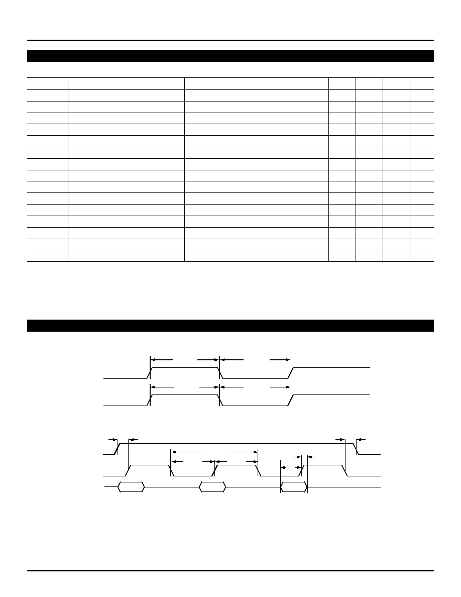
TIMING WAVEFORMS
t
REFPWL
REFCLK
t
REFPWH
t
CLKPWL
CLKOUT
PROGCS
t
SKP
t
SKPWH
t
SKPWL
t
DIS
PROGSK
PROGDI
t
DIH
t
SKCS
t
CSSK
Valid
Valid
Valid
t
CLKPWH
5
SY87739L
Micrel
FUNCTIONAL DESCRIPTION
General
The SY87739L AnyClockTM Fractional-N Synthesizer is
used in serial data streaming applications, where the
incoming data rate on a channel may vary, or where the
incoming data rate on a channel is unknown ahead of time.
In these situations, a valid output stream must still be
generated even in the absence of any edges on the
corresponding input stream. Up until now, designers had to
resort to sub-optimal solutions such as providing multiple
reference oscillators. Beyond the potential noise and EMI
issues, the designer has no way to future proof his circuit,
as it would prove near impossible to pre-provision all the
reference frequencies that might be needed after
deployment, yet are unknown at this time.
The SY87739L solves this problem by generating exact
frequencies for common data streaming protocols, all from
one 27MHz reference. If any of these protocols include
overhead due to use of common digital wrappers, The
SY87739L still generates the exact frequency required,
including the overhead.
Besides generating reference rates for common protocols
directly, the SY87739L also generates reference frequencies
for Micrel's SY87721L CDR/CMU, such that it will reliably
recover data at any rate between 28Mbps and 2,700Mbps
without any gaps.
A simple 3-wire MicroWireTM bit-serial interface loads a
configuration that describes the desired output reference
frequency. All common microcontrollers support this
MicroWireTM interface. Those microcontrollers that don't
support this interface in hardware can easily emulate the
interface in firmware.
The large set of possible frequencies that the SY87739L
generates, are divided into three classes. First, the sets of
frequencies that match a particular data streaming protocol
are in the "protocol" category. Second, the set of frequencies
that are guaranteed to be near enough to any arbitrary data
rate such that the SY87721L will lock are in the "picket
fence" category. Third, the set of frequencies that do not fit
into either of the first two categories is in the third category,
The SY87739L generates these important reference
frequencies through two tandem PLL circuits. The first PLL
uses a modified fractional-N approach to generate a rational
ratio frequency. This PLL is capable of generating all protocol
data rates, except for those that include FEC or digital
wrapper overhead. A second, more traditional P/Q
synthesizer optionally adjusts the output frequency of the
first, fractional-N synthesizer, to accommodate these FEC
or digital wrapper data rates.
The bit serial interface conveys 32 bits of configuration
data from a microcontroller to SY87739L. This simple
interface consists of an active high chip select, a serial
clock (2MHz or less) and a serial data input. Each clock
cycle one bit of configuration data transfers to SY87739L.
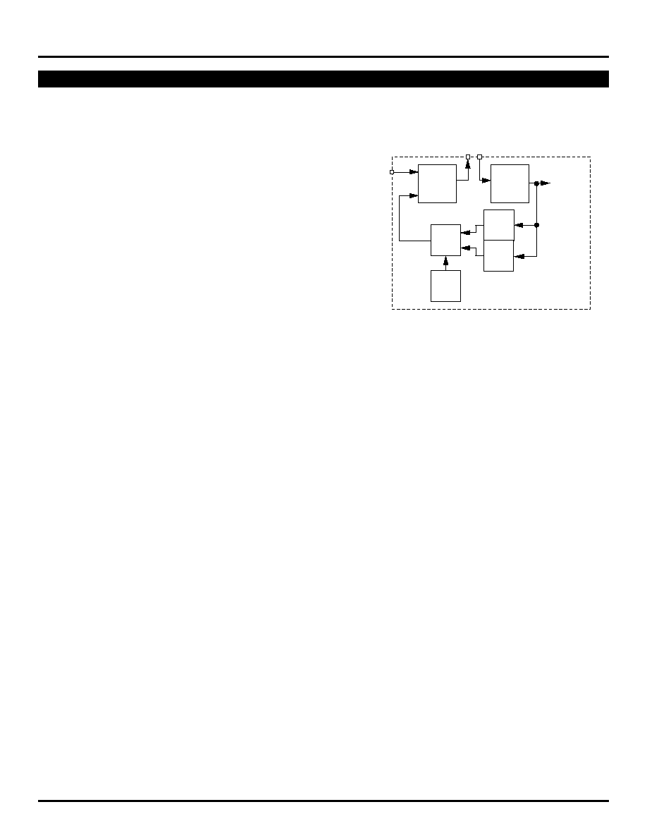
Circuit Description
The heart of SY87739L is its fractional-N synthesizer, as
shown in Figure 1.
Phase-
Frequency
Detector/
Charge
Pump
VCO
P
P-1
Mux
Control
Loop Filter
Input
Reference
Frequency
(f
REF
)
Output
Frequency
(f
FNOUT
)
Figure 1. Fractional-N Synthesizer Architecture
The two dividers in the feedback path always differ by
one count. That is, if one divider is set to divide by P = 5,
then the other divider divides by P≠1 = 4 . The mux choses
between the two based on the control circuit.
The idea behind the fractional-N approach is that every
input reference edge is used. Only those output edges that
are nearest to an input edge get fed back to the phase-
frequency comparator. In addition, the nearest output edges
are chosen in such a way that the net offset, over a number
of edges, zeroes out. It is the control circuit's job to drive
the mux such that only the "correct" edges get fed back.
In the above fractional-N circuit, if the output frequency
should be, for example, 5 times the input frequency, then P
is set to 5, and the control circuit sets the mux to only feed
back the output of the P divider.
If the output frequency should be, for example, 4
1
/
2
times
the input frequency, then the control circuit alternates evenly
between the P and the P≠1 divider output. For every two
input edges (one to compare against P, and another to
compare against P≠1), you will get 5 + 4 output edges,
yielding an output frequency 9/2 the input frequency.
Whereas P sets the integer part of the multiplication factor
from input to output frequency, the control circuit determines
the fractional part. By mixing the output of the P and P≠1
dividers correctly, the control circuit can fashion any output
frequency from P≠1 times the input to P times the input, as
long as that ratio can be expressed as a ratio of integers.