 | –≠–ª–µ–∫—Ç—Ä–æ–Ω–Ω—ã–π –∫–æ–º–ø–æ–Ω–µ–Ω—Ç: SY88923 | –°–∫–∞—á–∞—Ç—å:  PDF PDF  ZIP ZIP |
DESCRIPTION
s
Up to 2.5Gbps operation
s
Low noise
s
Chatter-Free LOS generation
s
Open Collector TTL LOS output
s
TTL /EN Input
s
Differential PECL inputs for data
s
Single power supply
s
Designed for use with SY88922 and SY88904 or
SY88905
s
Available in a tiny 10-pin (3mm) MSOP
The SY88923 limiting post amplifier with its high gain
and wide bandwidth is ideal for use as a post amplifier in
fiber-optic receivers with data rates up to 2.5Gbps. Signals
as small as 5mVp-p can be amplified to drive devices with
PECL inputs. The SY88923 generates a chatter-free Loss
of Signal (LOS) open collector TTL output.
The SY88923 incorporates a programmable level detect
function to identify when the input signal has been lost.
This information can be fed back to the /EN input of the
device to maintain stability under loss of signal condition.
Using LOS
LVL
pin, the sensitivity of the level detection can
be adjusted. The LOS
LVL
voltage can be set by connecting
a resistor divider between V
CC
and V
REF
. Figure 3 and
Figure 4 show the relationship between input level sensitivity
and the voltage set on LOS
LVL
. Figure 5 shows the
relationship between input level sensitivity and resistor
divider ratio.
The LOS output is a TTL open collector output that
requires a pull-up resistor for proper operation, Figure 1.
FEATURES
2.5Gbps HIGH-SPEED
LIMITING POST AMPLIFIER
SY88923
APPLICATIONS
s
1.25Gbps Gigabit Ethernet
s
531Mbps and 1062Mbps Fibre Channel
s
622Mbps SONET
s
Gigabit interface converter
s
2.5Gbps SDH/SONET
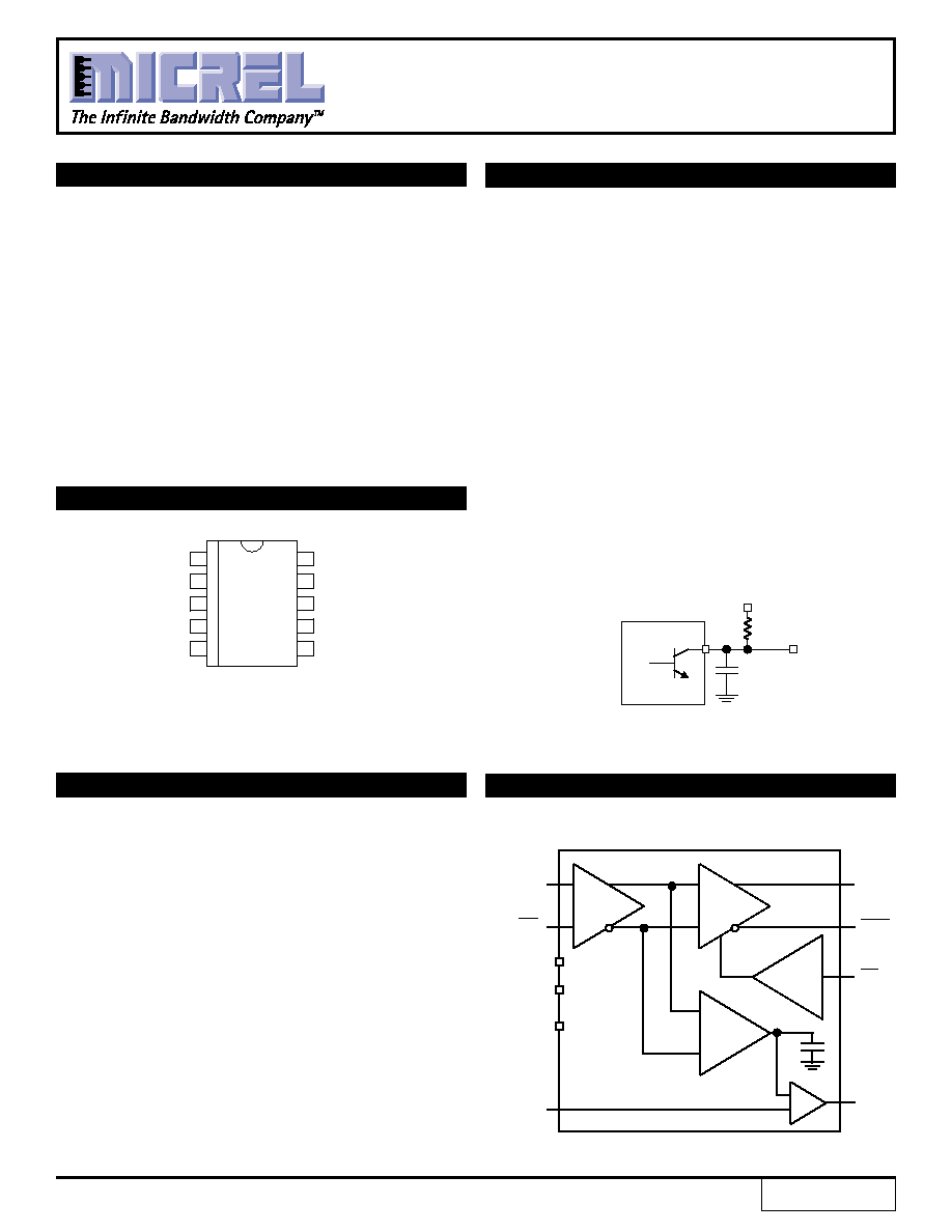
PIN CONFIGURATION
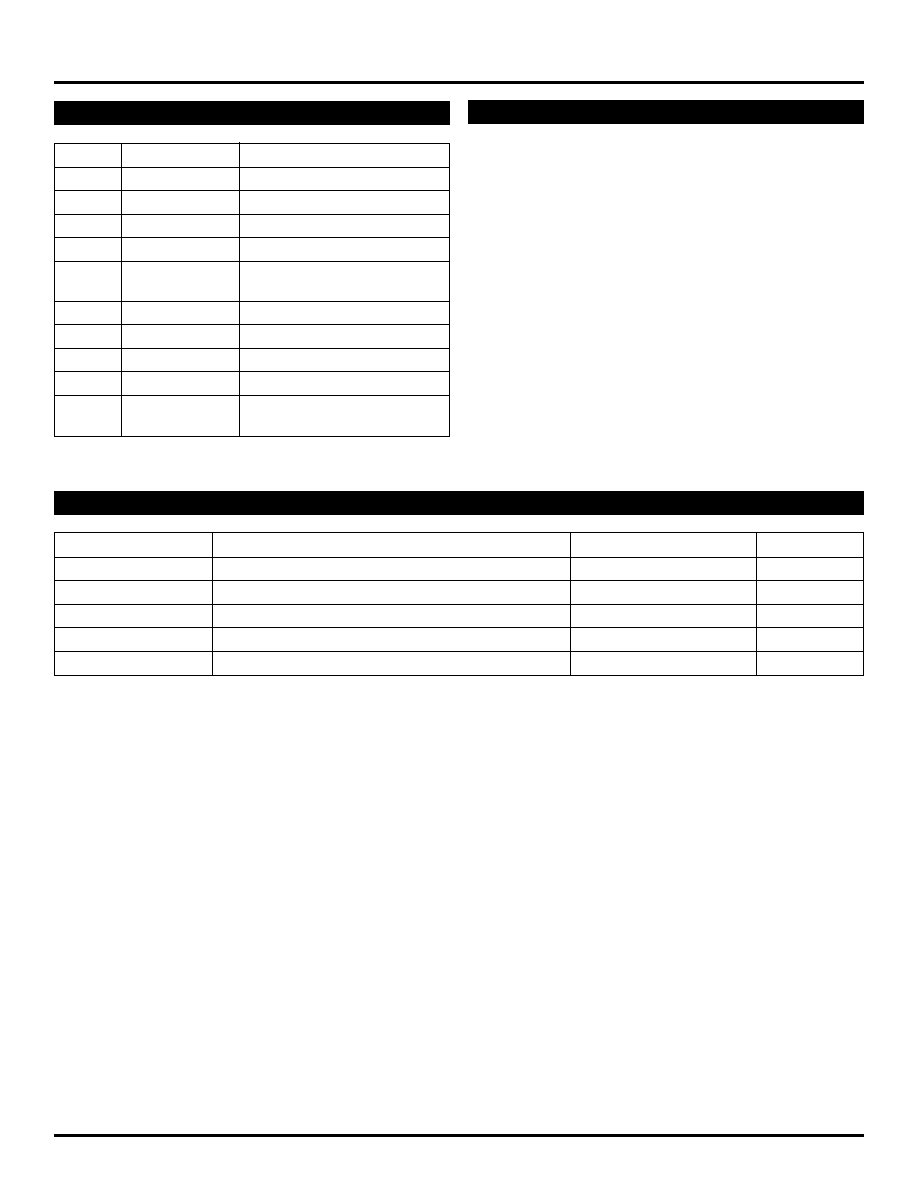
BLOCK DIAGRAM
1
/EN
D
IN
/D
IN
V
REF
LOS
LVL
10 V
CC
D
OUT
/D
OUT
LOS
GND
9
8
7
6
2
3
4
5
MSOP
K10-1
Figure 1. LOS Output with Desired Rise Time
SY88923
LOS
+5.0V
2k
Limiting
Amplifer
ECL
Buffer
D
IN
D
IN
V
REF
V
CC
GND
LOS
LVL
Enable
Level
Detect
D
OUT
D
OUT
EN
LOS
1
Rev.: C
Amendment: /1
Issue Date:
July 2000
2
SY88923
Micrel
Pin
Type
Function
D
IN
Data Input
Data Input
/D
IN
Data Input
Inverting Data Input
LOS
LVL
Input
LOS Limit Set
/EN
TTL Input
Output Enable (Active Low)
LOS
TTL Output
Loss of Signal Indicator
(Open Collector)
(Active High)
GND
Ground
Ground
/D
OUT
PECL Output
Inverting Data Output
D
OUT
PECL Output
Data Output
V
CC
Power Supply
Positive Power Supply
V
REF
Output
Reference Voltage Output for
LOS Level Set (see Fig. 3)
General
The SY88923 is an integrated limiting amplifier intended
for high-frequency fiber-optic applications. The circuit
connects to typical transimpedance amplifiers found within
a fiber-optics link. The linear signal output from a
transimpedance amplifier can contain significant amounts
of noise, and may vary in amplitude over time. The SY88923
limiting amplifier quantizes the signal and outputs a voltage-
limited waveform.
The /EN pin allows the user to disable the output signal
without removing the input signal.
PIN NAMES
GENERAL DESCRIPTION
Symbol
Rating
Value
Unit
V
CC
Power Supply Voltage
0 to +7.0
V
D
IN
, /D
IN
Input Voltage
0 to V
CC
V
D
OUT
, /D
OUT
Output Voltage (with 50
load)
V
CC
≠2.5, V
CC
+0.3
V
T
A
Operating Temperature Range
≠40 to +85
∞
C
T
store
Storage Temperature Range
≠55 to +125
∞
C
ABSOLUTE MAXIMUM RATINGS
(1)
NOTE:
1. Permanent device damage may occur if ABSOLUTE MAXIMUM RATINGS are exceeded. This is a stress rating only and functional operation is not implied
at conditions other than those detailed in the operational sections of this data sheet. Exposure to ABSOLUTE MAXIMUM RATlNG conditions for extended
periods may affect device reliability.
3
SY88923
Micrel
T
A
= ≠40
∞
C
T
A
= 0
∞
C
T
A
= +25
∞
C
T
A
= +85
∞
C
Symbol
Parameter
Min.
Max.
Min.
Max.
Min.
Typ.
Max.
Min.
Max.
Unit
I
CC
Power Supply Current
(1)
--
35
--
35
--
21
35
--
35
mA
I
IL
/EN Input LOW Current
≠0.3
(8)
--
≠0.3
(8)
--
≠0.3
(8)
--
--
≠0.3
(8)
--
mA
I
IH
/EN Input HIGH Current
--
20
(5)
--
20
(5)
--
--
20
(5)
--
20
(5)
µ
A
--
100
(6)
--
100
(6)
--
--
100
(6)
--
100
(6)
V
CMR
Common Mode Range
GND +2.0
V
CC
≠1.0
GND +2.0
V
CC
≠1.0
GND +2.0
--
V
CC
≠1.0
GND +2.0
V
CC
≠1.0
V
V
offset
Differential Output Offset
--
±
100
--
±
100
--
--
±
100
--
±
100
mV
LOS
LVL
LOS
LVL
Level
(2)
V
REF
V
CC
V
REF
V
CC
V
REF
--
V
CC
V
REF
V
CC
V
V
OL
LOS Output Low Level
(3)
--
0.5
--
0.5
--
--
0.5
--
0.5
V
I
OH
LOS Output Leakage
(4)
--
250
--
250
--
--
250
--
250
uA
V
OH
D
OUT
and /D
OUT
V
CC
≠1085
V
CC
≠880 V
CC
≠1025 V
CC
≠880 V
CC
≠1025 V
CC
≠955
V
CC
≠880
V
CC
≠1025
V
CC
≠880
mV
HIGH Output
V
OL
D
OUT
and /D
OUT
V
CC
≠1830 V
CC
≠1555 V
CC
≠1810 V
CC
≠1620 V
CC
≠1810 V
CC
≠1705 V
CC
≠1620 V
CC
≠1810 V
CC
≠1620
mV
LOW Output
V
REF
Reference Supply
(7)
V
CC
≠2.625 V
CC
≠2.325 V
CC
≠2.625 V
CC
≠2.325 V
CC
≠2.625 V
CC
≠2.475 V
CC
≠2.325 V
CC
≠2.625 V
CC
≠2.325
V
V
IH
/EN Input HIGH Voltage
2.0
--
2.0
--
2.0
--
--
2.0
--
V
V
IL
/EN Input LOW Voltage
--
0.8
--
0.8
--
--
0.8
--
0.8
V
NOTES:
1. No output load.
2. 2
23
-1 pattern.
3. I
OL
= + 2mA.
4. V
OH
= 5.5V.
DC ELECTRICAL CHARACTERISTICS
V
CC
= +5V
±
10%, R
LOAD
= 50
to V
CC
-2V, T
A
= ≠40
∞
C to +85
∞
C
5. V
IN
= 2.7.
6. V
IN
=V
CC.
7. I
REF
must be limited within ≠0.8mA (source) and 0.4mA (sink).
8. V
IN
= 0.5V
.
T
A
= ≠40
∞
C
T
A
= 0
∞
C
T
A
= +25
∞
C
T
A
= +85
∞
C
Symbol
Parameter
Min.
Max.
Min.
Max.
Min.
Typ.
Max.
Min.
Max.
Unit
Conditions
PSRR
Power Supply
(1)
--
--
--
--
--
35
--
--
--
dB
Input referred,
Rejection Ratio
55MHz
V
ID
Input Voltage Range
5
1800
5
1800
5
--
1800
5
1800 mVp-p
t
r,
t
f
Output Rise/Fall Time
--
175
--
175
--
--
175
--
175
ps
V
ID
> 100mVp-p
--
--
--
--
--
t
rin
,t
fin
--
--
--
V
ID
< 100mVp-p
V
OD
Differential Output
--
--
--
--
--
600
--
--
--
mV
V
ID
= 15mVp-p
Voltage Swing
(2)
--
--
--
--
--
200
--
--
--
mV
V
ID
= 5mVp-p
t
OFFL
LOS Release Time
(3)
--
0.5
--
0.5
--
0.1
0.5
--
0.5
µ
s
Minimum Input
t
OFFH
LOS Release Time
(4)
--
0.5
--
0.5
--
0.1
0.5
--
0.5
µ
s
Maximum Input
t
ONL
LOS Assert Time
(3)
--
0.5
--
0.5
--
0.2
0.5
--
0.5
µ
s
V
SR
LOS Sensitivity Range
5
50
5
50
5
--
50
5
50
mVp-p
2
23
-1 pattern
HYS
LOS Hysteresis
2
8
2
8
2
4.6
8
2
8
dB
AC ELECTRICAL CHARACTERISTICS
V
CC
= +5V
±
10%, R
LOAD
= 50
to V
CC
- 2V, T
A
= ≠40
∞
C to +85
∞
C
3. Input is a 200MHz square wave, tr < 300ps, 8mVp-p.
4. Input is a 200MHz square wave, tr < 300ps, 1.8Vp-p.
NOTES:
1. Input referred noise = RMS output noise/low frequency gain.
2. Input is a 622MHz square wave.
4
SY88923
Micrel
LOS Assert and Deassert Levels
vs LOS
LVL
0.00
10.00
20.00
30.00
40.00
50.00
60.00
70.00
80.00
90.00
100.00
2.53
2.65
2.77
2.90
3.02
3.14
3.27
3.39
3.52
3.64
3.76
3.89
4.01
4.13
4.26
4.38
4.51
4.63
4.75
4.88
5.00
LOS
LVL
(V)
Level (mV)
Deassert
Assert
Output Termination
The SY88923 outputs must be terminated with a 50
load to V
CC
≠ 2V (or thevenin equivalent).
Layout and PCB Design
Since the SY88923 is a high-frequency component,
performance can largely be determined by board layout
and design. A common problem with high-gain amplifiers is
feedback from the large swing outputs to the input via power
supply.
The SY88923 ground pin should be connected to the
circuit board ground. Use multiple PCB vias close to the
part to connect to ground. Avoid long, inductive runs which
can degrade performance.
DESIGN PROCEDURE
Figure 3. LOSLVL Circut
NOTE:
Resistor Divider = R2/ (R1 + R2)
R1 + R2
5k
Figure 2. Differential Input Configuration
D
IN+
D
IN≠
V
REF
50
50
0.1
µ
F
0.1
µ
F
0.1
µ
F
V
CC
R1
R2
LOS
LVL
V
REF
PERFORMANCE CURVE
Figure 4. 2
23
-1 Pattern
Figure 5. 2
23
-1 Pattern
0.00
0.05
0.10
0.15
0.20
0.25
0.30
0.35
0.40
0.45
0.50
0.55
0.60
0.65
0.70
0.75
0.80
0.85
0.90
0.95
1.00
Resistor Divider R2 / (R1 + R2)
Deassert
Assert
LOS Assert and Deassert Levels
vs Resistor Divide
0.00
10.00
20.00
30.00
40.00
50.00
60.00
70.00
80.00
90.00
100.00
Level (mV)
5
SY88923
Micrel
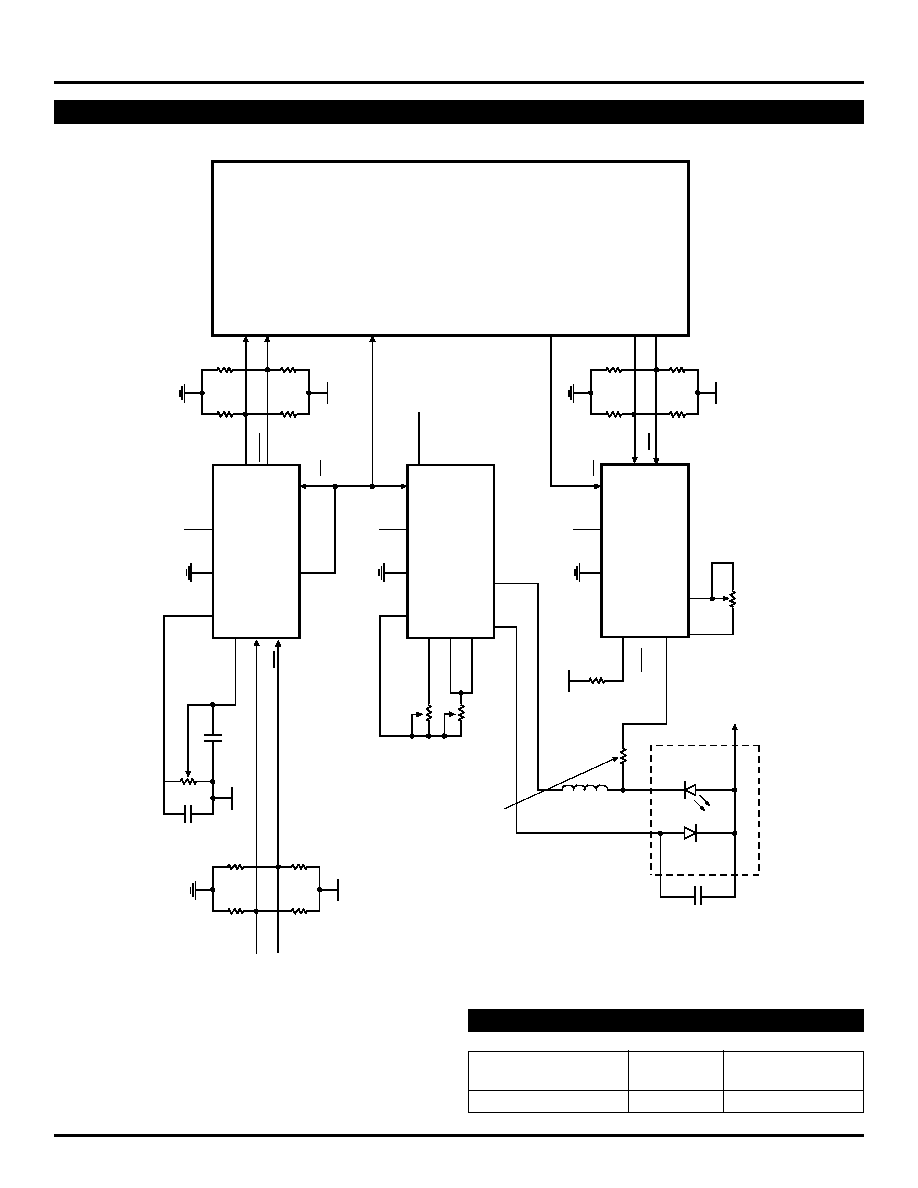
APPLICATION EXAMPLE FOR 3-CHIP SET SOLUTION
D
IN
D
IN
GBIC Terminal
EN
RX_DATA
≠
RX_DATA+
TX_DATA
≠
TX_DATA+
RX_LOS
ENABLE/DISABLE
200
V
CC
GND
200
68
68
V
CC
EN
V
CC
GND
V
CC
GND
D
OUT
D
OUT
200
200
68
68
V
CC
OUT
OUT
D
IN
24
V
CC
R
EXT
R
SER
Laserdiode
Photodiode
V
REF
MD
I
BIAS
LOS
OUT
LOS
IN
D
IN
LOS
LVL
I
BIAS SET
SY88905
20k
20k
1000pF
BLM21A102S
Laser
Module
I
BIAS FB
I
PIN SET
LOS
V
REF
SY88923
0.1µF
20k
0.1µF
130
130
82
82
V
CC
20k
SY88922
V
REF
R
SET
The value of RSER
depends on the Laser Diode.
V
CC
V
CC
PRODUCT ORDERING CODE
Ordering
Package
Operating
Code
Type
Range
SY88923KC
K10-1
Commercial