The SY88932L is the smallest laser driver with
programmable modulation current for SONET/SDH
applications up to 3.2Gbps. The device accepts either
CML level or AC-coupled PECL inputs. The SY88932L
provides modulation current of up to 60mA for FP (Fabry-
Perot) or DFB (Distributed Feedback) lasers. The devices
incorporates an active low TTL /EN function which shuts
off modulation current when high.
FEATURES
DESCRIPTION
SY88932L
Final
3.3V 3.2Gbps
SONET/SDH LASER DRIVER
WITH OUTPUT DISABLE
s
Up to 3.2Gbps operation
s
Modulation current to 60mA
s
Rise/fall times 65ps typical
s
Input 50
internally terminated to V
CC
s
TTL /EN with internal 75k
pull-down
s
Designed for use with MIC3000 optical transceiver
management IC
s
Voltage programmable laser modulation current
s
Single 3.3V power supply
s
Operating temperature range of ≠40
∞
C to 85
∞
C
s
Available in tiny 16-pin MLFTM package
1
Rev.: A
Amendment: /0
Issue Date:
Nov. 15, 2002
APPLICATIONS
s
Fiber optical module
s
Transponder
s
XAUI CWDM
s
SONET/SDH transmission system
s
Add-drop mux
s
Metro area network
s
2.5Gbps optical transmitter
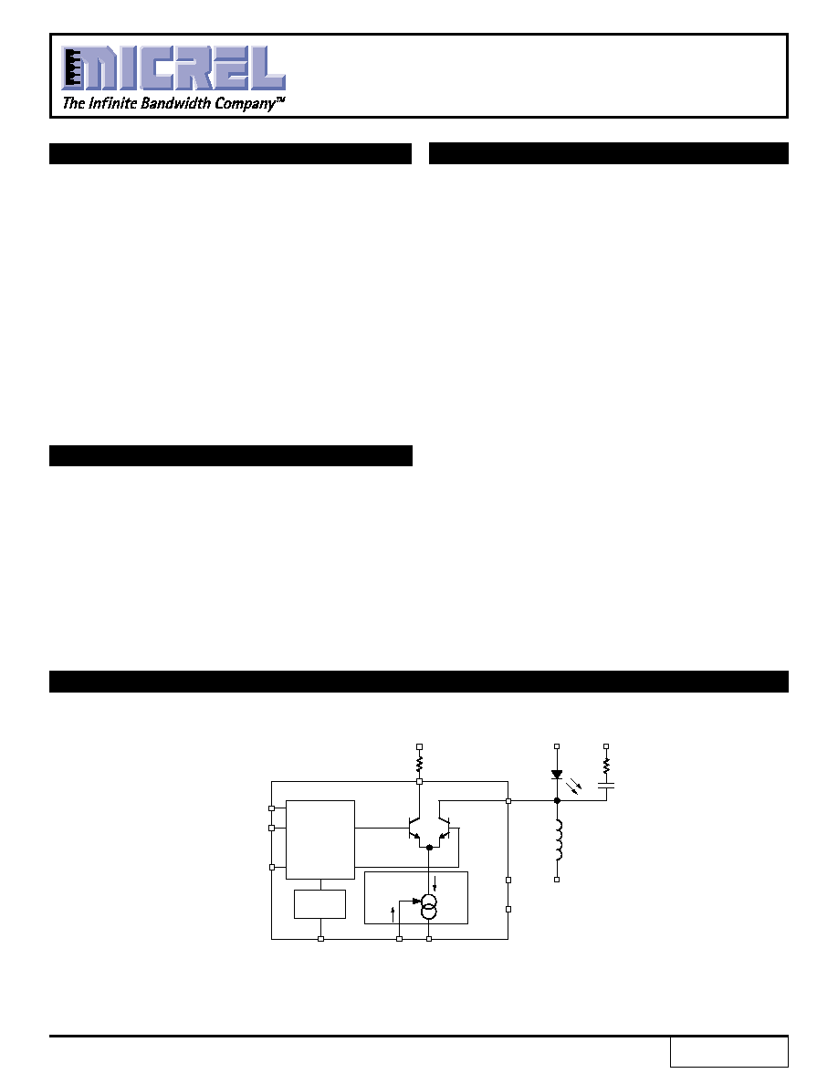
BLOCK DIAGRAM
D
IN
/D
IN
/EN
Internal
Logic
V
REF
GND
V
CC
OUT
/OUT
R
EXT
V
CC
GND
I
BIAS
V
CC
V
CC
V
CNTRL
V
REF
Generator
I
MOD
Modulation
Control
MLF and
MicroLeadFrame are trademarks of Amkor Technology, Inc.
2
SY88932L
Micrel
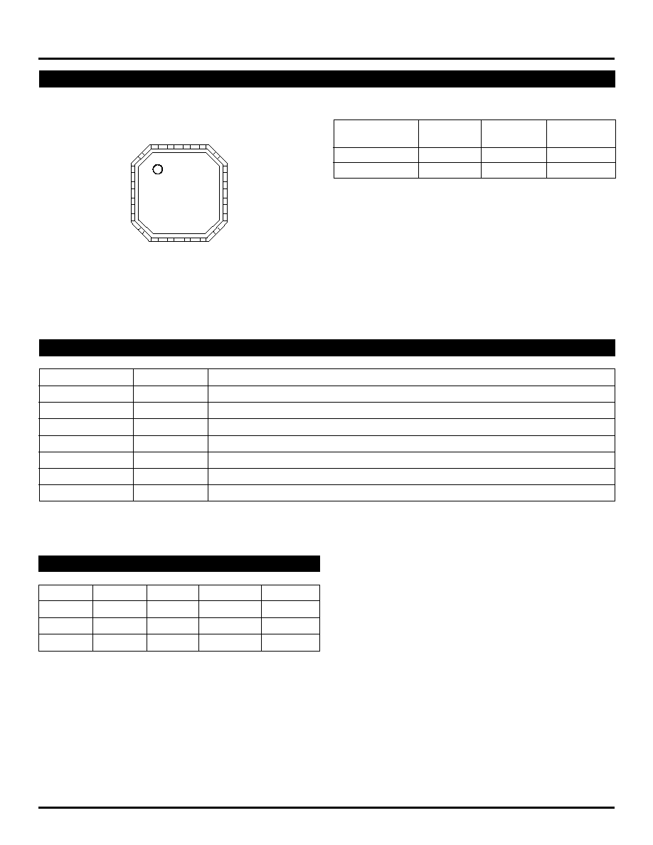
PACKAGE/ORDERING INFORMATION
Ordering Information
Package
Operating
Package
Part Number
Type
Range
Marking
SY88932LMI
MLF-16
Industrial
932L
SY88932LMITR*
MLF-16
Industrial
932L
*Tape and Reel
Pin Number
Pin Name
Pin Function
2, 3
DIN, /DIN
NRZ differential data (inputs), CML terminated interface with 50
to V
CC
.
1, 4, 7, 8, 13
GND
Ground.
5, 6,
VCC
Positive power supply.
9, 10, 11, 12,
OUT, /OUT
Open collector (outputs) from the modulation driver.
14
VREF
Voltage reference, nominally 1.25V.
`
15
VCNTRL
Voltage control of I
MOD
. 5k
input impedance. See
"Typical Operating Characteristics."
16
/EN
Enable: TTL compatible active low input with 75k
pull-down resistor.
PIN DESCRIPTION
1
2
3
4
12
11
10
9
16 15 14 13
5
6
7
8
GND
DIN
/DIN
GND
OUT
OUT
/OUT
/OUT
GND
VREF
VCNTRL
/EN
GND
GND
VCC
VCC
16-Pin MLFTM
D
/D
/EN
OUT
(NOTE 2)
/OUT
L
H
L
H
L
H
L
L
L
H
X
X
H
H
L
TRUTH TABLE
(NOTE 1)
Note 1.
L = LOW, H = HIGH, X = don't care.
Note 2.
I
OUT
I
MOD_OFF
when /EN is HIGH.
3
SY88932L
Micrel
V
CC
= 3.0 to 3.6V, GND = 0V, T
A
= ≠40
∞
C to +85
∞
C; Typical values at V
CC
= 3.3V, T
A
= 25
∞
C.
Symbol
Parameter
Condition
Min
Typ
Max
Units
I
CC
Power Supply Current
Note 1
65
90
mA
I
MOD
Modulation Current Range
10
60
mA
I
MOD_OFF
Modulation Off Current
/EN
= V
IHEN
200
µ
A
V
IDDIN
Input Differential Voltage (D
IN
, /D
IN
)
Note 2
400
800
1600
mVpp
V
IHEN
Input HIGH Voltage (/EN)
2.0
V
V
ILEN
Input LOW Voltage (/EN)
0.8
V
V
OUT
Voltage (OUT, /OUT)
Note 3
V
CC
≠1.5
V
CC
V
V
REF
Reference Voltage
Note 4
1.2
1.25
1.3
V
Note 1.
Excluding I
MOD
. I
MOD
set for 60mA.
Note 2.
V
IDDIN
is the voltage required to guarantee a stable logic level. For logic "1", D
IN
must be
V
2
IDDIN
above /D
IN
. For stable logic "0", D
IN
must
be
V
2
IDDIN
below /D
IN
.
Note 3.
OUT and /OUT are current outputs. This specification defines the voltage range that the user must guarantee these pins remain within for
proper operation.
Note 4.
V
REF
intended to source/sink
|5mA|.
DC ELECTRICAL CHARACTERISTICS
Absolute Maximum Ratings
(Note 1)
Supply Voltage (V
CC
) .................................. ≠0.5V to +4.0V
CML Input Voltage (V
IN
) ............... V
CC
≠1.0V to V
CC
+0.5V
TTL Control Input Voltage (V
IN
) .......................... 0V to V
CC
Lead Temperature (soldering, 10 sec.) ................... +300
∞
C
Storage Temperature (T
S
) ....................... ≠65
∞
C to +150
∞
C
Operating Ratings
(Note 2)
Supply Voltage (V
CC
) .................................. +3.0V to +3.6V
Ambient Temperature (T
A
) ......................... ≠40
∞
C to +85
∞
C
Junction Temperature (T
J
) ........................................ 120
∞
C
Package Thermal Resistance
MLFTM
(
JA
) still air ...................................................... 59
∞
C/W
(
JB
) still air ..................................................... 32
∞
C/W
Note 1.
Permanent device damage may occur if ABSOLUTE MAXIMUM RATINGS are exceeded. This is a stress rating only and functional operation
is not implied at conditions other than those detailed in the operational sections of this data sheet. Exposure to ABSOLUTE MAXIMUM
RATlNG conditions for extended periods may affect device reliability.
Note 2.
The data sheet limits are not guaranteed if the device is operated beyond the operating ratings.
4
SY88932L
Micrel
V
CC
= 3.0 to 3.6V, GND = 0V, T
A
= ≠40
∞
C to +85
∞
C; Typical values at V
CC
= 3.3V, T
A
= 25
∞
C.
Symbol
Parameter
Condition
Min
Typ
Max
Units
D
J
Deterministic Jitter
Notes 2, 3
20
ps
p-p
t
r
,
t
f
Output Rise/Fall Times
Note 2
65
100
ps
(20% to 80%)
Note 1.
AC characteristics are guaranteed by design and characterization.
Note 2.
I
MOD
= 40mA, 25
resistors each tied from OUT and /OUT to V
CC
.
Note 3.
I
MOD
= 40mA, 2.5Gbps, 0-1 pattern, BW = 12KHz to 20MHz.
AC ELECTRICAL CHARACTERISTICS
(NOTE 1)
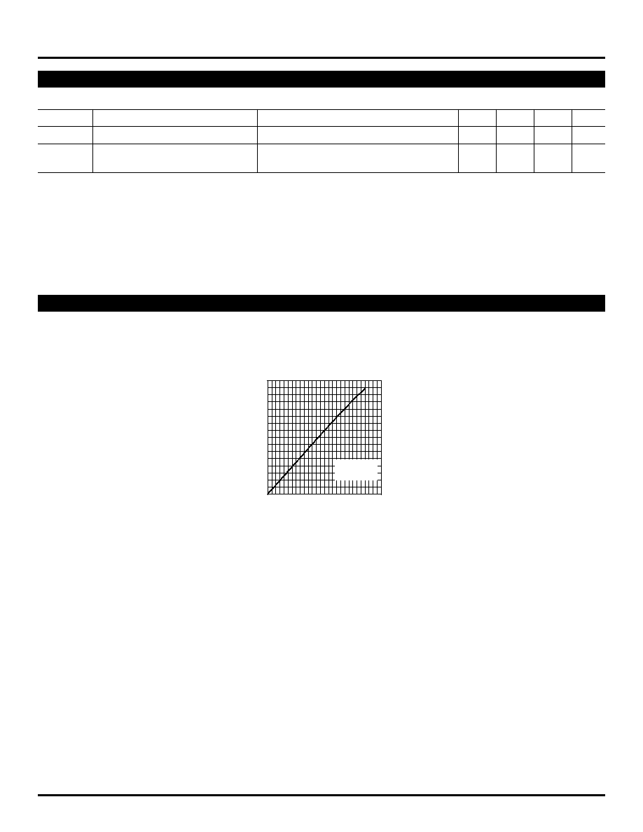
TYPICAL OPERATING CHARACTERISTICS
0
10
20
30
40
50
60
70
80
0
0.2 0.4 0.6 0.8
1
1.2 1.4
I
MOD
(mA)
V
CNTRL
(V)
I
MOD
vs. V
CNTRL
V
CC
= 3.3V
T
A
= 25
∞
C
5
SY88932L
Micrel
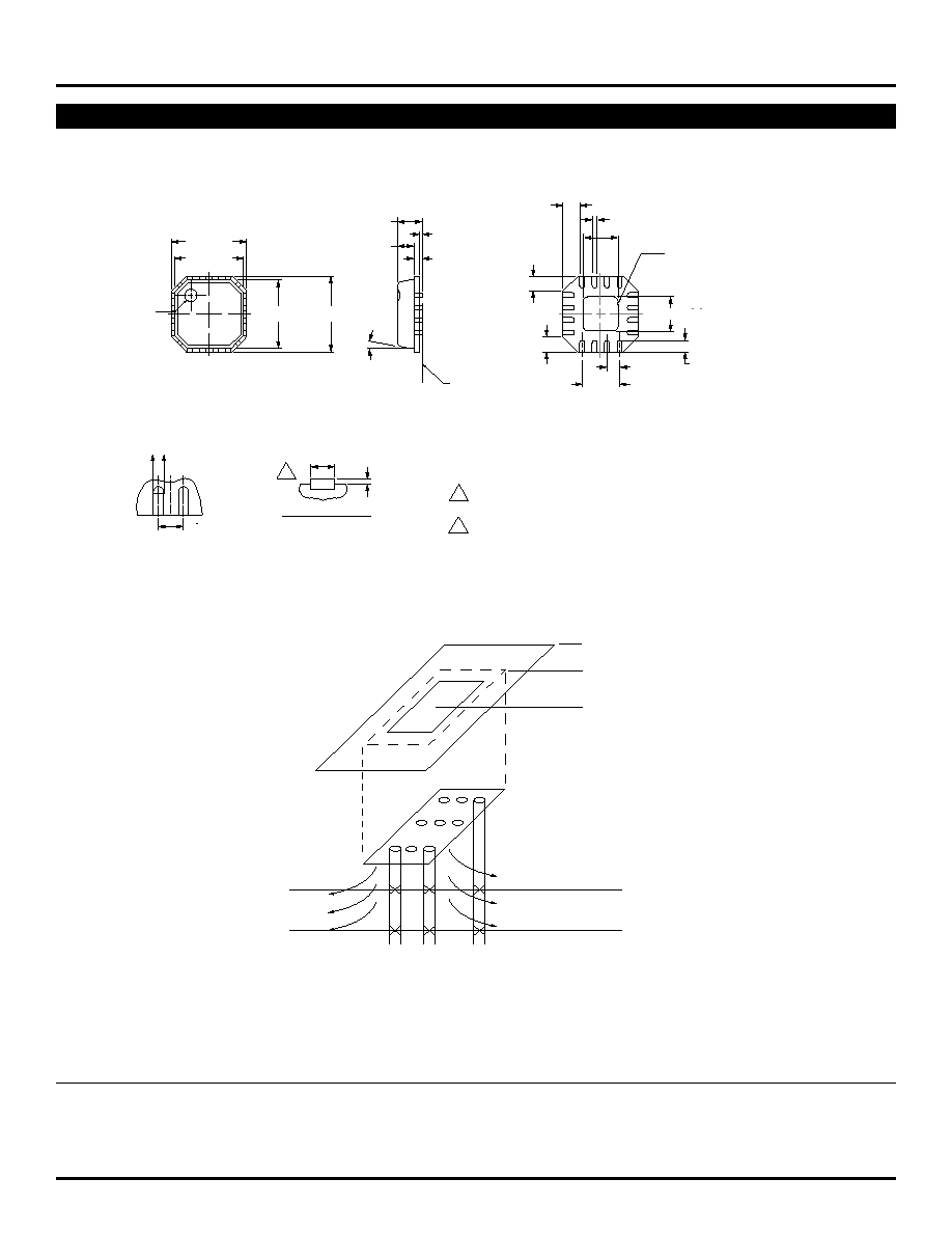
16 LEAD EPAD-
MicroLeadFrameTM (MLF-16)
3.00BSC
2.75BSC
0.50 DIA
3.00BSC
12
∞
max
SEATING
PLANE
2.75BSC
16
1
1
2
3
4
N
2
3
4
0.85
+0.15
≠0.65
0.65
+0.15
≠0.65
0.01
+0.04
≠0.01
0.23
+0.07
≠0.05
0.01
+0.04
≠0.01
0.42
+0.18
≠0.18
0.42
+0.18
≠0.18
0.23
+0.07
≠0.05
1.60
+0.10
≠0.10
PIN 1 ID
0.5 BSC
1.5 REF
0.42
+0.18
≠0.18
1.60
+0.10
≠0.10
0.40
+0.05
≠0.05
0.20 REF.
0.5BSC
SECTION "C-C"
SCALE: NONE
FOR EVEN TERMINAL/SIDE
TOP VIEW
BOTTOM VIEW
1. DIMENSIONS ARE IN mm.
2. DIE THICKNESS ALLOWABLE IS 0.305mm MAX.
3. PACKAGE WARPAGE MAX 0.05mm.
4. THIS DIMENSION APPLIES TO PLATED TERMINAL AND IS MEASURED
BETWEEN 0.20mm AND 0.25mm FROM TIP.
5. APPLIES ONLY FOR TERMINALS
C C
CL
4
Rev. 02
Rev. 01
Package
EP- Exposed Pad
Die
CompSide Island
Heat Dissipation
Heavy Copper Plane
Heavy Copper Plane
V
EE
V
EE
Heat Dissipation
PCB Thermal Consideration for 16-Pin MLFTM Package
MICREL, INC.
1849 FORTUNE DRIVE
SAN JOSE, CA 95131
USA
TEL
+ 1 (408) 944-0800
FAX
+ 1 (408) 944-0970
WEB
http://www.micrel.com
This information is believed to be accurate and reliable, however no responsibility is assumed by Micrel for its use nor for any infringement of patents or
other rights of third parties resulting from its use. No license is granted by implication or otherwise under any patent or patent right of Micrel, Inc.
© 2002 Micrel, Incorporated.