1
SY88983V
Micrel, Inc.
M9999-020205
hbwhelp@micrel.com or (408) 955-1690
February 2005
DESCRIPTION
s
Multi-Rate up to 3.2Gbps operation
s
Wide gain-bandwidth product
∑ 38dB differential gain
∑ 2.2GHz 3dB bandwidth
s
Low noise 50
CML data outputs
∑ 800mV
pp
output swing
∑ 60ps edge rates
∑ 5ps
rms
typ. random jitter
∑ 15ps
pp
typ. deterministic jitter
s
Chatter-free Signal Detect (SD) output
∑ 4.6dB electrical hysteresis
∑ OC-TTL output with internal 5k
pull-up resistor
s
Programmable SD sensitivity using single external
resistor
s
Internal 50
data input termination
s
TTL EN input allows feedback from SD
s
Wide operating range
∑ Single 3.3V
±
10% or 5V
±
10% power supply
∑ ≠40
∞
C to +85
∞
C industrial temperature range
s
Available in tiny 10-pin MSOP (3mm) and 16-pin MLFTM
(3mm
◊◊
◊◊
◊
3mm) packages
s
NOT RECOMMENDED for New Designs!
FEATURES
3.3V/5V 3.2Gbps CML
LOW-POWER LIMITING
POST AMPLIFIER w/TTL SD
SY88983V
APPLICATIONS
s
1.25Gbps and 2.5Gbps Gigabit Ethernet
s
1.062Gbps and 2.125Gbps Fibre Channel
s
155Mbps, 622Mbps, 1.25Gbps and 2.5Gbps
SONET/SDH
s
Gigabit interface converter (GBIC)
s
Small form factor (SFF) and small form factor pluggable
(SFP) transceivers
s
Parallel 10G Ethernet
s
High-gain line driver and line receiver
MLF and
MicroLeadFrame are trademarks of Amkor Technology, Inc.
The SY88983V low-power limiting post amplifier is
designed for use in fiber optic receivers. The device connects
to typical transimpedance amplifiers (TIAs). The linear signal
output from TIAs can contain significant amounts of noise
and may vary in amplitude over time. The SY88983V
quantizes these signals and outputs typically 800mV
pp
voltage-limited waveforms.
The SY88983V operates from a single +3.3V
±
10% or
+5V
±
10% power supply, over the industrial temperature of
≠40
∞
C to +85
∞
C. With its wide bandwidth and high gain,
signals with data rates up to 3.2Gbps and as small as
10mV
pp
can be amplified to drive devices with CML inputs
or AC-coupled PECL inputs.
The SY88983V generates a signal detect (SD) open-
collector TTL output with internal 5k
pull-up resistor. A
programmable signal detect level set pin (SD
LVL
) sets the
sensitivity of the input amplitude detection. SD asserts high
if the input amplitude rises above the threshold set by SD
LVL
and de-asserts low otherwise. SD can be fed back to the
enable (EN) input to maintain output stability under a loss-
of-signal condition. EN de-asserts the true output signal
without removing the input signal. Typically, 4.6dB SD
hysteresis is provided to prevent chattering.
All support documentation can be found on Micrel's web
site at www.micrel.com.
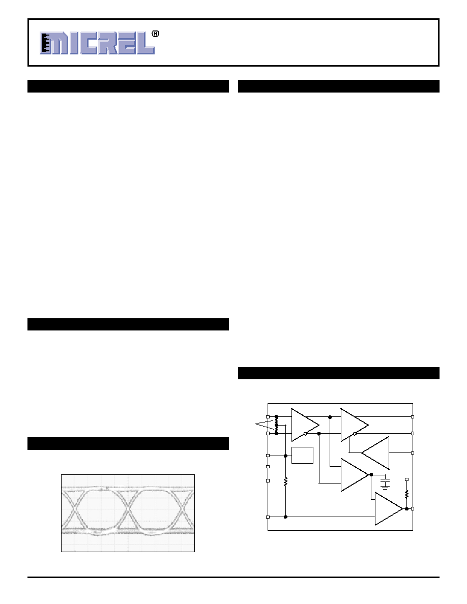
FUNCTIONAL BLOCK DIAGRAM
3.3V, 25∞C, 10mV
PP
Input
@2.5Gbps 2
23
≠1 PRBS, R
LOAD
= 50
to V
CC
TIME (100ps/div.)
Output Swing
(75mV/div
.
)
TYPICAL PERFORMANCE
Limiting
Amplifer
CML
Buffer
GND
2.8k
50
TTL
Buffer
Level
Detect
EN
SD
D
IN
/D
IN
V
REF
V
CC
V
CC
SD
LVL
D
OUT
/D
OUT
5k
OC-TTL
Buffer
V
CC
--1.3V
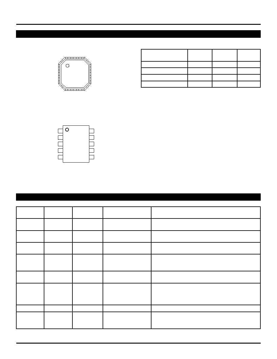
2
SY88983V
Micrel, Inc.
M9999-020205
hbwhelp@micrel.com or (408) 955-1690
February 2005
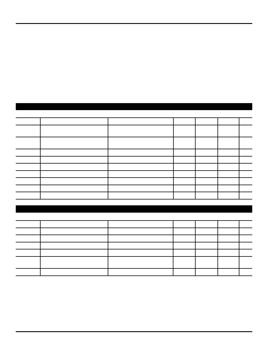
PACKAGE/ORDERING INFORMATION
Ordering Information
Package
Operating
Package
Part Number
Type
Range
Marking
SY88983VKI
K10-1
Industrial
983V
SY88983VKITR
(1)
K10-1
Industrial
983V
SY88983VMI
MLF-16
Industrial
983V
SY88983VMITR
(1)
MLF-16
Industrial
983V
Note:
1. Tape and Reel.
1
EN
DIN
/DIN
VREF
SDLVL
10 VCC
DOUT
/DOUT
SD
GND
9
8
7
6
2
3
4
5
10-Pin MSOP (K10-1)
1
2
3
4
12
11
10
9
16 15 14 13
5
6
7
8
DIN
GND
GND
/DIN
DOUT
GND
GND
/DOUT
VCC
SDL
VL
EN
VCC
VCC
SD
VREF
VCC
16-Pin MLFTM (MLF-16)
PIN DESCRIPTION
Pin Number
Pin Number
(MSOP)
(MLFTM)
Pin Name
Type
Pin Function
1
15
EN
TTL Input:
Enable: De-asserts true data output when low.
Default is high.
2, 3
1, 4
DIN, /DIN
Differential Data Input
Differential data input. Each pin internally terminates to
V
REF
through 50
.
4
6
VREF
Reference Voltage: Bypass with 0.01
µ
F low ESR
capacitor from V
REF
to V
CC
to stabilize SD
LVL
and V
REF
.
5
14
SDLVL
Input:
Signal Detect Level Set: A resistor from this pin to V
CC
Default is
sets the threshold for the data input amplitude at which
maximum sensitivity.
the SD output will be asserted.
6
2, 3, 10, 11,
GND
Ground
Device ground. Exposed pad must be connected to same
Exposed Pad
potential as ground pins for MLF-16.
7
7
SD
Open-Collector:
Signal Detect: Asserts high when the data input
TTL Output with
amplitude rises above the threshold set by SD
LVL
.
internal 5k
pull-up
resistor.
8, 9
9, 12
DOUT, /DOUT
Differential CML Output
Differential data output.
10
5, 8, 13, 16
VCC
Power Supply
Positive power supply. Bypass with 0.1
µ
F
0.01
µ
F low
ESR capacitors. 0.01
µ
F capacitors should be as close to
V
CC
pins as possible.
3
SY88983V
Micrel, Inc.
M9999-020205
hbwhelp@micrel.com or (408) 955-1690
February 2005
Absolute Maximum Ratings
(1)
Supply Voltage (V
CC
) ....................................... 0V to +7.0V
EN, SD
LVL
Voltage ................................................. 0 to V
CC
D
IN
, /D
IN
Current ......................................................
±
10mA
D
OUT
, /D
OUT
Current ................................................
±
25mA
SD Current .................................................................
±
5mA
V
REF
Current ..............................................................
±
1mA
Storage Temperature (T
S
) ....................... ≠65
∞
C to +150
∞
C
Lead Temperature (soldering, 10 sec.) ..................... 220
∞
C
Operating Ratings
(2)
Supply Voltage (V
CC
) .............................. +3.0V to +3.6V or
............................................................ +4.5V to +5.5V
Ambient Temperature (T
A
) ......................... ≠40
∞
C to +85
∞
C
Junction Temperature (T
J
) ....................... ≠40
∞
C to +120
∞
C
Package Thermal Resistance
(3)
MLFTM
(
JA
) Still-Air .................................................... 61
∞
C/W
(
JB
) ................................................................ 38
∞
C/W
MSOP
(
JA
) Still-Air .................................................. 113
∞
C/W
(
JB
) ................................................................ 74
∞
C/W
V
CC
= 3.0V to 3.6V or 4.5V to 5.5V; R
LOAD
= 50
to V
CC
; T
A
= ≠40
∞
C to +85
∞
C; typical values at V
CC
= 3.3V, T
A
= 25
∞
C.
Symbol
Parameter
Condition
Min
Typ
Max
Units
I
CC
Power Supply Current
(4)
3.3V
19
28
mA
5V
21
31
mA
I
CC
Power Supply Current
(5)
3.3V
32
53
mA
5V
38
58
mA
V
REF
V
REF
Voltage
V
CC
≠1.3
V
SD
LVL
SD
LVL
Level
V
REF
V
CC
V
V
OH
Output HIGH Voltage
Note 6
V
CC
≠0.020 V
CC
≠0.005
V
CC
V
V
OL
Output LOW Voltage
Note 6
V
CC
≠0.400 V
CC
≠0.275
V
V
OFFSET
Differential Output Offset
±
80
mV
Z
O
Single-Ended Output Impedance
40
50
60
Z
I
Single-Ended Input Impedance
40
50
60
DC ELECTRICAL CHARACTERISTICS
V
CC
= 3.0V to 3.6V or 4.5V to 5.5V; R
LOAD
= 50
to V
CC
; T
A
= ≠40
∞
C to +85
∞
C; typical values at V
CC
= 3.3V, T
A
= 25
∞
C.
Symbol
Parameter
Condition
Min
Typ
Max
Units
V
OH
SD Output HIGH Level
Sourcing 100
µ
A
2.4
V
CC
V
V
OL
SD Output LOW Level
Sinking 2mA
0.5
V
V
IH
EN Input HIGH Voltage
2.0
V
V
IL
EN Input LOW Voltage
0.8
V
I
IH
EN Input HIGH Current
V
IN
= 2.7V
20
µ
A
V
IN
= V
CC
100
µ
A
I
IL
EN Input LOW Current
V
IN
= 0.5V
≠0.3
mA
Notes:
1. Permanent device damage may occur if
"Absolute Maximum Ratings" are exceeded. This is a stress rating only and functional operation is not
implied at conditions other than those detailed in the operational sections of this data sheet. Exposure to
"Absolute Maximum Ratings" conditions for
extended periods may affect device reliability.
2. The data sheet limits are not guaranteed if the device is operated beyond the operating ratings.
3. Thermal performance assumes use of 4-layer PCB. If applicable, exposed pad must be soldered (or equivalent) to the device's most negative
potential on the PCB.
4. Excludes current of CML output stage. See
"Detailed Description."
5. Total device current with no output load.
6. Output levels are based on a 50
to V
CC
load impedance. If the load impedance is different, the output level will be changed.
TTL DC ELECTRICAL CHARACTERISTICS
4
SY88983V
Micrel, Inc.
M9999-020205
hbwhelp@micrel.com or (408) 955-1690
February 2005
V
CC
= 3.0V to 3.6V or 4.5V to 5.5V; R
LOAD
= 50
to V
CC
; T
A
= ≠40
∞
C to +85
∞
C; typical values at V
CC
= 3.3V, T
A
= 25
∞
C.
Symbol
Parameter
Condition
Min
Typ
Max
Units
HYS
SD Hysteresis
Note 7
2
4.6
8
dB
PSRR
Power Supply Rejection Ratio
35
dB
t
OFF
SD Release Time
0.1
0.5
µ
s
t
ON
SD Assert Time
0.2
0.5
µ
s
t
r
, t
f
Differential Output Rise/Fall Time
60
120
ps
(20% to 80%)
Note 8
t
JITTER
Deterministic
Note 9
15
ps
p-p
Random
5
ps
rms
V
ID
Differential Input Voltage Swing
10
1800
mV
p-p
V
OD
Differential Output Voltage Swing
Note 10
550
800
mV
p-p
V
SR
SD Sensitivity Range
Note 11
10
50
mV
p-p
A
V(Diff)
Differential Voltage Gain
32
38
dB
B
≠3dB
3dB Bandwidth
2.2
GHz
S
21
Single-Ended Small Signal-Gain
26
32
dB
Notes:
7. Electrical signal.
8. With input signal V
ID
> 50mV
p-p
and 50
load.
9. Deterministic jitter measured using K28.5 pattern at 2.488Gbps, V
ID
= 10mV
p-p
. Random jitter measured using K28.7 pattern at 2.488Gbps, V
ID
=
10mV
p-p
.
10. Input is a 200MHz square wave, t
r
< 300ps, 50
load. V
ID
14mV
p-p
.
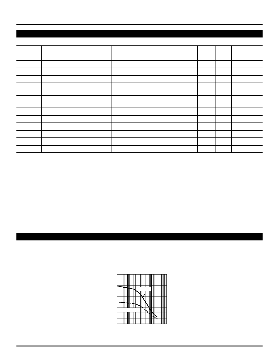
11. This is the detectable range of input amplitudes that can de-assert SD. The input amplitude to assert SD is 2≠8dB higher than the de-assert
amplitude. See
"Typical Operating Characteristics" for a graph showing how to choose a particular R
SDLVL
for a particular SD de-assert, and its
associated assert, amplitude.
AC ELECTRICAL CHARACTERISTICS
TYPICAL OPERATING CHARACTERISTICS
0
10
20
30
40
50
60
70
80
90
10
100
1000
10000 100000
V
ID
(mV
P-P
)
R
SDLVL
SD Assert/Deassert Level
vs. R
SDLVL
ASSERT
DEASSERT
V
CC
= 3.3V, GND = 0V, T
A
= 25
∞
C unless otherwise stated.

5
SY88983V
Micrel, Inc.
M9999-020205
hbwhelp@micrel.com or (408) 955-1690
February 2005
DETAILED DESCRIPTION
The SY88983V low power limiting post amplifier operates
from a single +3.3V or +5V power supply, over temperatures
from ≠40
∞
C to +85
∞
C. Signals with data rates up to 3.2Gbps
and as small as 10mV
p-p
can be amplified. Figure 1 shows
the allowed input voltage swing. The SY88983V generates
an SD output, allowing feedback to EN for output stability.
SD
LVL
sets the sensitivity of the input amplitude detection.
Input Amplifier/Buffer
The SY88983V's inputs are internally terminated with 50
to V
REF
. Unless they are not affected by this internal
termination scheme, upstream devices need to be
AC-coupled to the SY88983V's inputs. Figure 2 shows a
simplified schematic of the input stage.
The high sensitivity of the input amplifier allows signals
as small as 10mV
p-p
to be detected and amplified. The
input amplifier allows input signals as large as 1800mV
p-p
.
Input signals are linearly amplified with a typically 38dB
differential voltage gain. Since it is a limiting amplifier, the
SY88983V outputs typically 800mV
p-p
voltage-limited
waveforms for input signals that are greater than 10mV
p-p
.
Applications requiring the SY88983V to operate with high-
gain should have the upstream TIA placed as close as
possible to the SY88983V's input pins to ensure the best
performance of the device.
Output Buffer
The SY88983V's CML output buffer is designed to drive
50
lines. The output buffer requires appropriate termination
for proper operation. An external 50
resistor to V
CC
or
equivalent for each output pin provides this. Figure 3 shows
a simplified schematic of the output stage and includes an
appropriate termination method. Of course, driving a
downstream device with a CML input that is internally
terminated with 50
to V
CC
eliminates the need for external
termination. As noted in the previous section, the amplifier
outputs typically 800mV
p-p
waveforms across 25
total
loads. The output buffer, thus, switches typically 16mA tail-
current. Figure 4 shows the power supply current
measurement, which excludes the 16mA tail-current.
Signal Detect
The SY88983V generates a chatter-free signal detect
(SD) open-collector TTL output with internal 5k
pull-up
resistor as shown in Figure 5. SD is used to determine that
the input amplitude is large enough to be considered a
valid input. SD asserts high if the input amplitude rises
above the threshold set by SD
LVL
and de-asserts low
otherwise. SD can be fed back to the enable (EN) input to
maintain output stability under a loss-of-signal condition.
EN de-asserts low the true output signal without removing
the input signals. Typically, 4.6dB SD hysteresis is provided
to prevent chattering.
Signal Detect-Level Set
A programmable signal detect-level set pin (SD
LVL
) sets
the threshold of the input amplitude detection. Connecting
an external resistor between V
CC
and SD
LVL
sets the voltage
at SD
LVL
. This voltage ranges from V
CC
to V
REF
. The
external resistor creates a voltage divider between V
CC
and
V
REF
as shown in Figure 6. If desired, an appropriate
external voltage may be applied rather than using a resistor.
The smaller the external resistor, implying a smaller voltage
difference from SD
LVL
to V
CC
, lowers the SD sensitivity.
Hence, larger input amplitude is required to assert SD.
"Typical Operating Characteristics" shows the relationship
between the input amplitude detection sensitivity and the
SD
LVL
setting resistor.
Hysteresis
The SY88983V provides typically 4.6dB SD electrical
hysteresis. By definition, a power ratio measured in dB is
10log(power ratio). Power is calculated as V
2
IN
/R for an
electrical signal. Hence, the same ratio can be stated as
20log(voltage ratio). While in linear mode, the electrical
voltage input changes linearly with the optical power and
hence, the ratios also change linearly. Therefore, the optical
hysteresis in dB is half the electrical hysteresis in dB given
in the data sheet. The SY88983V provides typically 2.3dB
SD optical hysteresis. As the SY88983V is an electrical
device, this data sheet refers to hysteresis in electrical terms.
With 4.6dB SD hysteresis, a voltage factor of 1.7 is required
to assert SD from its de-assert value.