 | –≠–ª–µ–∫—Ç—Ä–æ–Ω–Ω—ã–π –∫–æ–º–ø–æ–Ω–µ–Ω—Ç: SY89112U | –°–∫–∞—á–∞—Ç—å:  PDF PDF  ZIP ZIP |

SY89113U
2.5V Low Jitter, Low Skew 1:12 LVDS Fanout
Buffer with 2:1 Input MUX and Internal Termination
Precision Edge is a registered trademark of Micrel, Inc.
MLF and
Micro
LeadFrame are trademarks of Amkor Technology, Inc.
Micrel Inc. ∑ 2180 Fortune Drive ∑ San Jose, CA 95131 ∑ USA ∑ tel +1 (408) 944-0800 ∑ fax + 1 (408) 474-1000 ∑ http://www.micrel.com
March 2005
M9999-032905
hbwhelp@micrel.com
or (408) 955-1690
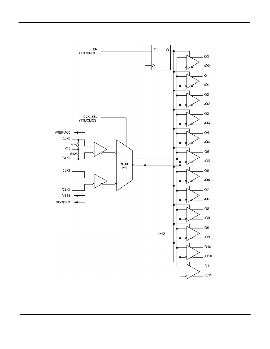
General Description
The SY89113U is a 2.5V low jitter, low skew, 1:12
LVDS fanout buffer optimized for precision telecom
and enterprise server distribution applications. The
input includes a 2:1 MUX for clock switchover
applications. Unlike other multiplexers, this input
includes a unique isolation design that minimizes
channel-to-channel crosstalk. The SY89113U
distributes clock frequencies from DC to >1GHz
guaranteed over temperature and voltage. The
SY89113U incorporates a synchronous output enable
(EN) so that the outputs will only be enabled/disabled
when they are already in the LOW state.
CLK0 differential input includes Micrel's unique, 3-pin
input termination architecture that directly interfaces to
any differential signal (AC- or DC-coupled) as small as
100mV (200mV
PP
) without any level shifting or
termination resistor networks in the signal path.
CLK1 differential input includes a new version of
Micrel's unique, Any-Input architecture that directly
interfaces with single-ended TTL/CMOS logic
(including 3.3V logic), single-ended LVPECL,
differential (AC- or DC-coupled) LVDS, HSTL, CML,
and LVPECL logic levels as small as 200mV
(400mV
PP
). CLK1 input requires external termination.
LVDS output swing 325mV into 100 with extremely
fast rise/fall time guaranteed to be less than 250ps.
The SY89113U operates from a 2.5V±5% supply and
is guaranteed over the full industrial temperature
range of -40∞C to +85∞C. The SY89113U is part of
Micrel's high-speed, Precision Edge
Æ
product line.
All support documentation can be found on Micrel's
web site at:
www.micrel.com.
Precision Edge
Æ
Features
∑ Selects between 1 of 2 inputs, and provides 12
precision, low skew LVDS output copies
∑ Guaranteed AC performance over temperature and
voltage:
≠ DC to >1GHz throughput
≠ <975ps propagation delay CLK0-to-Q
≠ <250ps rise/fall time
≠ <25ps output-to-output skew
∑ Ultra-low jitter design:
≠ <1ps
RMS
random jitter
≠ <10ps
PP
total jitter (clock)
≠ <1ps
RMS
cycle-to-cycle jitter
≠ <0.7ps
RMS
crosstalk induced jitter
∑ Unique, patent-pending 2:1 input MUX provides
superior isolation to minimize channel-to-channel
crosstalk
∑ CLK0 input features a unique, patent-pending input
termination and VT pin that accepts AC- and DC-
coupled inputs (CML, LVPECL, LVDS)
∑ CLK1 accepts virtually any logic standard:
≠ Single-ended: TTL/CMOS (including 3.3V logic),
LVPECL
≠ Differential: LVPECL, LVDS, CML, HSTL
∑ 325mV LVDS-compatible output swing
∑ Power supply: 2.5V +5%
∑ Industrial temperature range ≠40∞C to +85∞C
∑ Available in 44-pin (7mm x 7mm) MLFTM package
Applications
∑ Multi-processor
server
∑ SONET/SDH clock/data distribution
∑ Fibre
Channel
distribution
∑ Gigabit Ethernet clock distribution
Micrel, Inc.
SY89113U
March 2005
M9999-032905
hbwhelp@micrel.com
or (408) 955-1690
2
Functional Block Diagram
Micrel, Inc.
SY89113U
March 2005
M9999-032905
hbwhelp@micrel.com
or (408) 955-1690
3
Ordering Information
(1)
Part Number
Package Type
Operating
Range
Package Marking
Lead
Finish
SY89113UMG
MLF-44
Industrial
SY89113U with Pb-Free bar-line indicator
NiPdAu
Pb-Free
SY89113UMGTR
(2)
MLF-44
Industrial
SY89113U with Pb-Free bar-line indicator
NiPdAu
Pb-Free
Notes:
1. Contact factory for die availability. Dice are guaranteed at T
A
= 25∞C, DC Electricals only.
2. Tape
and
Reel.
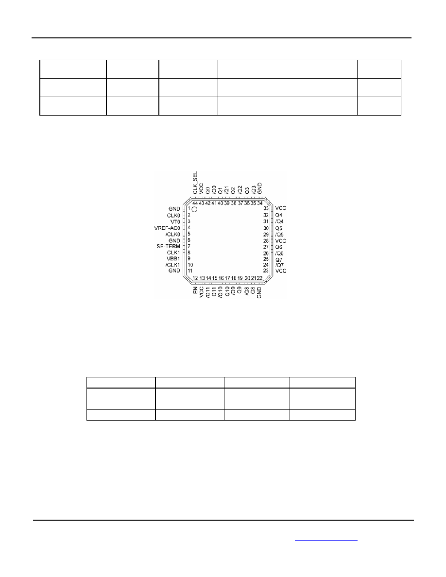
Pin Configuration
44-Pin MLF
TM
(MLF-44)
Truth Table
EN CLK_SEL Q
/Q
H L
CLK0
/CLK0
H H
CLK1
/CLK1
L X
L
(1)
H
(1)
Note:
1. Transition occurs on next negative transition of the non-inverted input.
Micrel, Inc.
SY89113U
March 2005
M9999-032905
hbwhelp@micrel.com
or (408) 955-1690
4
Pin Description
Pin Number
Pin Name
Pin Function
1, 6, 11, 22, 34
GND,
Exposed Pad
Ground. GND pins and exposed pad must both be connected to the most negative
potential of chip the ground.
2, 5
CLK0, /CLK0
Differential Inputs: This input pair is a differential signal input to the device. Input
accepts AC- or DC-coupled signals as small as 100mV (200mV
PP
). Each pin of the
pair internally terminates to a VT pin through 50. Note that this input defaults to an
indeterminate state if left open. Please refer to the "CLK0 Input Interface
Applications" section for more details.
3 VT0
Input Termination Center-Tap: Each side of the differential input pair CLK0, /CLK0
terminates to the VT pin. The VT pin provides a center-tap to a termination network
for maximum interface flexibility. See "CLK0 Input Interface Applications" section for
more details. For DC-coupled CML or LVDS inputs, the VT pin is left floating.
4 VREF-AC0
Reference Voltage: This output biases to V
CC
≠1.2V. It is used when AC-coupling the
input CLK0. For AC-coupled applications, connect VREF-AC0 to the VT0 pin and
bypass with 0.01µF low ESR capacitor to V
CC
. See "CLK0 Input Interface
Applications" section for more details. Maximum sink/source current is ±1.5mA. Due
to the limited drive capability, the VREF-AC0 pin is only intended to drive its
respective input pin.
7 SE-TERM
Input Termination Pin: When CLK1 is driven by a single-ended TTL/CMOS signal, tie
this pin to GND. In all other modes, let this pin float. See "CLK1 Interface
Applications" section for more details.
8, 10
CLK1, /CLK1
Differential Inputs: This input pair is a differential signal input to the device. This input
accepts Any-Logic standard as small as 200mV (400mV
PP
). Note that this input
defaults to an indeterminate state if left open. Tie either the true or the complement
input to ground while the other input is floating. This input can be used for single-
ended signals (including TTL/CMOS signals from a 3.3V driver). See "CLK1 Input
Interface Applications" section for more details.
9 VBB1
Reference Voltage: This output biases to V
CC
≠1.425V. VBB1 is designed to act as a
switching reference for the CLK1 and /CLK1 inputs when configured in single-ended
PECL input mode. VBB1 can be used for AC-coupling of CLK1, see Figure 4d for
details. Maximum sink/source current is ±1.5mA. Due to the limited drive capability,
the VBB1 pin is only intended to drive its respective input pin.
12 EN
This single-ended, TTL/CMOS-compatible input functions as a synchronous output
enable. The synchronous enable ensures that enable/disable will only occur when
the outputs are in a logic LOW state. Note that this input is internally connected to a
25k pull-up resistor and will default to logic HIGH state (enable) if left open.
13, 23, 28,
33, 43
VCC
Positive power supply. Bypass with 0.1µF//0.01µF low ESR capacitors and place as
close to the VCC pins as possible.
44 CLK_SEL
This single-ended, TTL/CMOS-compatible input selects the inputs to the multiplexer.
Note that this input is internally connected to a 25k pull-up resistor and will default
to logic HIGH state if open.
42, 41
40, 39
38, 37
36, 35
32, 31
30, 29
27, 26
25, 24
21, 20
19, 18
17, 16
15, 14
Q0, /Q0
Q1, /Q1
Q2, /Q2
Q3, /Q3
Q4, /Q4
Q5, /Q5
Q6, /Q6
Q7, /Q7
Q8, /Q8
Q9, /Q9
Q10, /Q10
Q11, /Q11
Differential LVDS Outputs: These LVDS output pairs are the precision, low skew
copies of the selected input. Please refer to the, "Truth Table" below for details.
Unused output pairs should be terminated with 100 across the pair. Each output is
designed to drive 325mV into 100. See the "LVDS Output Interface Applications"
section for more details.
Micrel, Inc.
SY89113U
March 2005
M9999-032905
hbwhelp@micrel.com
or (408) 955-1690
5
Absolute Maximum Ratings
(1)
Supply Voltage (V
CC
) .......................... ≠0.5V to +4.0V
Input Voltage
(Differential Input CLK0, CLK1
(4, 5)
).. ≠0.5V to V
CC
Current on Reference Voltage Outputs
Source or sink current on VREF-AC0, VBB1.....±2mA
Termination Current
Source or sink current on VT0................±100mA
Input Current
Source or sink current on CLK0, /CLK0 ...±50mA
Lead Temperature (soldering, 20 sec.) .......... +260∞C
Storage Temperature (T
s
) ................. ≠65∞C to 150∞C
Operating Ratings
(2)
Supply Voltage (V
CC
).................. +2.375V to +2.625V
Ambient Temperature (T
A
)................ ≠40∞C to +85∞C
Package Thermal Resistance
(3)
MLFTM
(
JA
)
Still-Air ................................................ 24∞C/W
MLFTM
(
JB
)
Junction-to-Board ................................. 8∞C/W
DC Electrical Characteristics
(6)
T
A
= ≠40∞C to +85∞C, unless otherwise stated.
Symbol Parameter
Condition
Min
Typ
Max
Units
V
CC
Power
Supply
2.375
2.625 V
I
CC
Power Supply Current
No load, max. V
CC
240
330
mA
R
IN
Input
Resistance
(CLK0-to-V
T
)
45 50 55
R
DIFF_IN
Differential Input Resistance
(CLK0-to-/CLK0)
90 100 110
Input High Voltage
(CLK0, /CLK0)
1.2
V
CC
V
(CLK1, /CLK1)
Note 4
0.2
V
CC
V
V
IH
Note
5
1.2
3.6
Input Low Voltage
(CLK0, /CLK0)
0.1
V
CC
V
(CLK1, /CLK1)
Note 4
0.2
V
V
IL
Note
5
0
V
Input Voltage Swing
(CLK0, /CLK0)
See Figure 1a.
0.1 V
CC
V
V
IN
(CLK1, /CLK1)
See Figure 1a.
0.2
V
Differential Input Voltage Swing
|CLK0-to-/CLK0|
See Figure 1b.
0.2
V
V
DIFF_IN
|CLK1-to-/CLK1|
See Figure 1b.
0.4
V
V
T0
CLK0-to-V
T0
(CLK0, /CLK0)
1.28
V
V
REF-AC0
Output Reference Voltage
V
CC
≠1.3 V
CC
≠1.2 V
CC
≠1.1 V
V
BB1
Output Reference Voltage
V
CC
≠1.525 V
CC
≠1.425 V
CC
≠1.325 V
Notes:
1. Permanent device damage may occur if absolute maximum ratings are exceeded. This is a stress rating only and functional operation is not
implied at conditions other than those detailed in the operational sections of this data sheet. Exposure to absolute maximum ratings
conditions for extended periods may affect device reliability.
2. The data sheet limits are not guaranteed if the device is operated beyond the operating ratings.
3. Package thermal resistance assumes exposed pad is soldered (or equivalent) to the devices most negative potential on the PCB.
JA
and
JB
values are determined for a 4-layer board in still-air, unless otherwise stated.
4. SE-TERM not connected.
5. Using single-ended TTL/CMOS input signals, SE-TERM connects to GND. See Figure 4f.
6. The circuit is designed to meet the DC specifications shown in the above table after thermal equilibrium has been established.