 | –≠–ª–µ–∫—Ç—Ä–æ–Ω–Ω—ã–π –∫–æ–º–ø–æ–Ω–µ–Ω—Ç: SY89200U | –°–∫–∞—á–∞—Ç—å:  PDF PDF  ZIP ZIP |
1
SY89200U
Micrel
M9999-061704
hbwhelp@micrel.com or (408) 955-1690
ULTRA-PRECISION 1:8 LVDS
FANOUT WITH THREE
˜
1/
˜
2/
˜
4
CLOCK DIVIDER OUTPUT BANKS
Precision Edge
SY89200U
Rev.: A
Amendment: /0
Issue Date:
June 2004
DESCRIPTION
s
Three low-skew LVDS output banks with
programmable
˜
1,
˜
2 and
˜
4 divider options
s
Three independently programmable output banks
s
Guaranteed AC performance over temperature and
voltage:
∑ Accepts a clock frequency up to 1.5GHz
∑ <900ps IN-to-OUT propagation delay
∑ <150ps rise/fall time
∑ <50ps bank-to-bank phase offset
s
Ultra-low jitter design:
∑ <1ps
rms
random jitter
∑ <10ps
pp
total jitter (clock)
s
Patent-pending input termination and VT pin accepts
DC- and AC-coupled inputs (CML, PECL, LVDS)
s
LVDS-compatible outputs
s
CMOS/TTL-compatible output enable (EN) and
divider select control
s
2.5V
±
5% power supply
s
≠40
∞
C to +85
∞
C temperature range
s
Available in 32-pin (5mm
◊◊
◊◊
◊
5mm) MLFTM package
FEATURES
APPLICATIONS
s
All SONET/SDH applications
s
All Fibre Channel applications
s
All Gigabit Ethernet applications
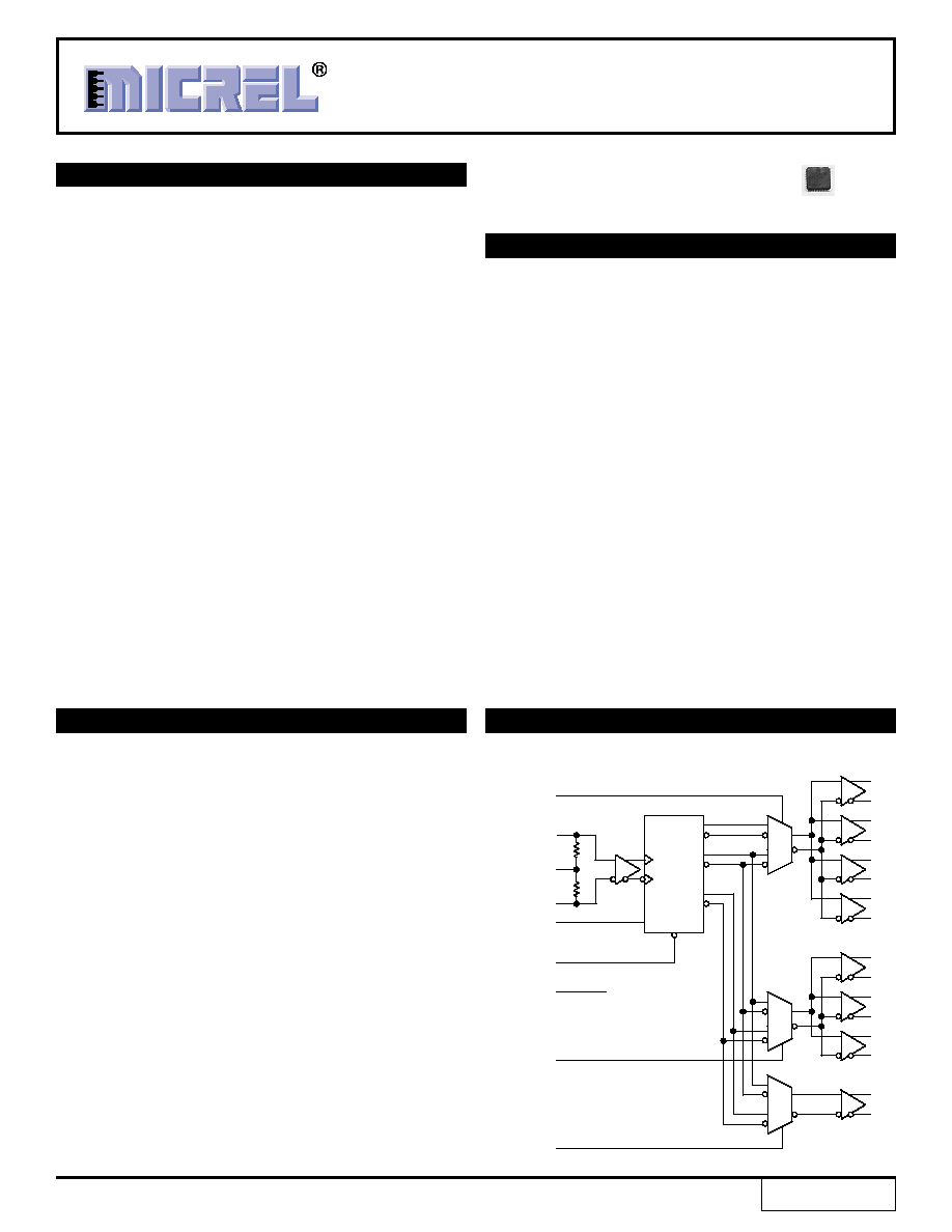
The SY89200U is a 2.5V precision, high-speed, integrated
clock divider and LVDS fanout buffer capable of handling
clocks up to 1.5GHz. Optimized for communications
applications, the three independently controlled output banks
are phase matched and can be configured for pass through
(
˜
1),
˜
2 or
˜
4 divider ratios.
The differential input includes Micrel's unique, 3-pin input
termination architecture that allows the user to interface to
any differential signal (AC or DC-coupled) as small as
200mV
pp
without any level shifting or termination resistor
networks in the signal path. The low-skew, low-jitter outputs
are LVDS compatible with extremely fast rise/fall times
guaranteed to be less than 150ps.
The EN (enable) input guarantees that the
˜
1,
˜
2 and
˜
4
outputs will start from the same state without any runt pulse
after an asynchronous master reset (MR) is asserted. This
is accomplished by enabling the outputs after a four-clock
delay to allow the counters to synchronize.
The SY89200U is part of a Micrel's Precision EdgeTM
product family. All support documentation can be found at
Micrel's web site at www.micrel.com.
FUNCTIONAL BLOCK DIAGRAM
Precision EdgeTM
MicroLead MLF is a trademark of Amkor Technology
Precision Edge is a trademark of Micrel, Inc.
2:1
MUX
2:1
MUX
2:1
MUX
1:4 LVDS
Fanout
1:3 LVDS
Fanout
LVDS
Output
˜1
˜2
˜4
DIVSEL1
(TTL/CMOS)
DIVSEL2
(TTL/CMOS)
DIVSEL3
(TTL/CMOS)
Select ˜2 or ˜4
Select ˜2 or ˜4
/MR
(TTL/CMOS)
EN
(TTL/CMOS)
V
REF-AC
IN
/IN
V
T
Q0
/Q0
Q1
/Q1
Q2
/Q2
Q3
/Q3
Q4
/Q4
Q5
/Q5
Q6
/Q6
Q7
/Q7
50
50
Select ˜1 or ˜2
2
SY89200U
Micrel
M9999-061704
hbwhelp@micrel.com or (408) 955-1690
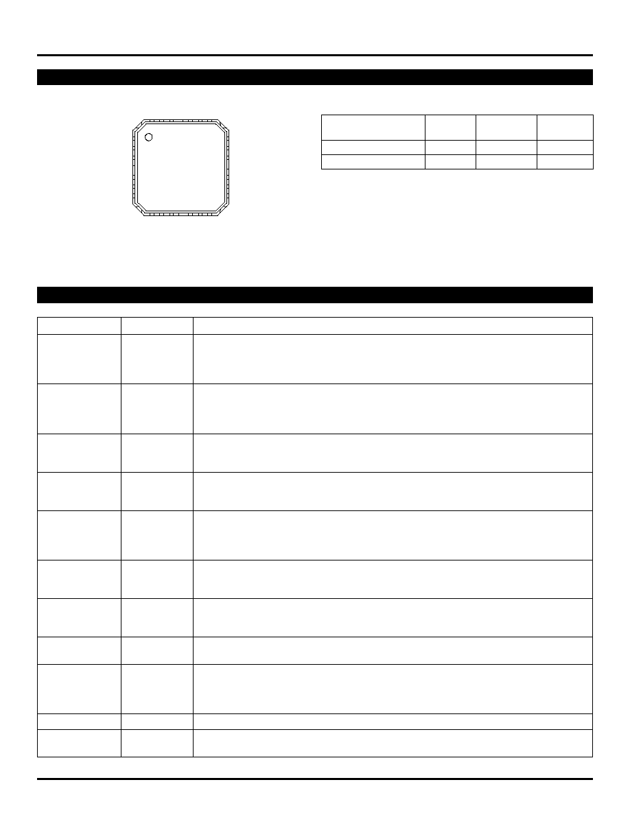
PACKAGE/ORDERING INFORMATION
Ordering Information
(1)
Package
Operating
Package
Part Number
Type
Range
Marking
SY89200U
MLF-32
Industrial
SY89200U
SY89200UTR
(2)
MLF-32
Industrial
SY89200U
Notes:
1. Contact factory for die availability. Dice are guaranteed at T
A
= 25
∞
C,
DC Electricals Only.
2. Tape and Reel.
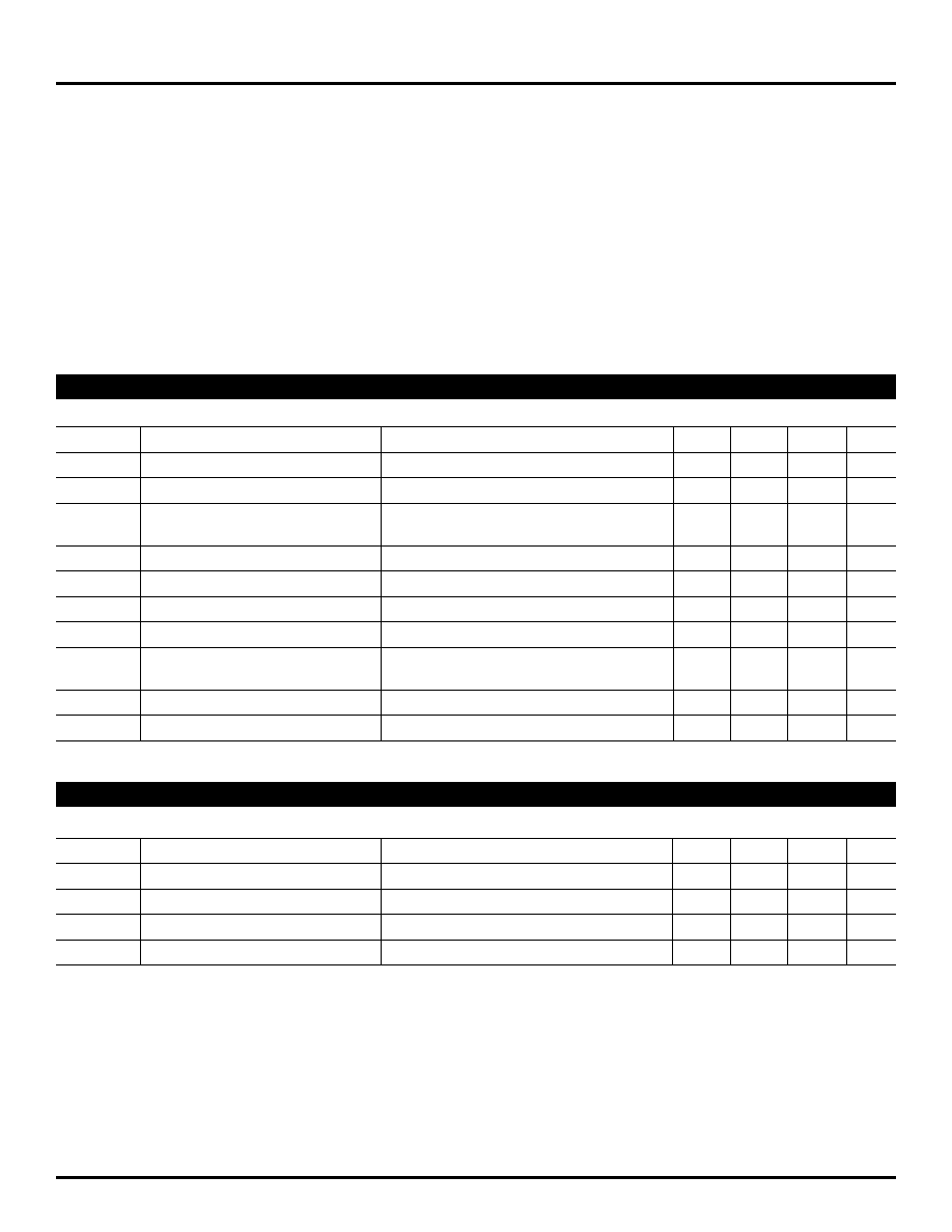
Pin Number
Pin Name
Pin Function
3, 6
IN, /IN
Differential Input: This input pair is the differential signal input to the device. This input
accepts AC- or DC-coupled signals as small as 100mV. The input pair internally terminates
to a VT pin through 50
. Note that these inputs will default to an indeterminate state if left
open. Please refer to the "Input Interface Applications" section for more details.
2
DIVSEL1
Single-Ended Inputs: These TTL/CMOS inputs select the divide ratio for each of the three
7
DIVSEL2
banks of outputs. Note that each of these inputs is internally connected to a 25k
pull-up
8
DIVSEL3
resistor and will default to a logic HIGH state if left open. The input switching threshold is
V
CC
/2.
4
VT
Input Termination Center-Tap: Each side of the differential input pair terminates to the VT
pin. The VT pin provides a center-tap to a termination network for maximum interface
flexibility. See "Input Interface Applications" section for more details.
5
VREF-AC
Reference Voltage: This output biases to V
CC
≠1.2V. It is used for AC-coupling inputs IN
and /IN. For AC-coupled applications, connect VREF-AC directly to the VT pin. Bypass with
0.01
µ
F low ESR capacitor to V
CC
. Maximum sink/source capability is 0.5mA.
9
EN
Single-Ended Input: This TTL/CMOS input disables and enables the Q0 ≠ Q7 outputs. This
input is internally connected to a 25k
pull-up resistor and will default to a logic HIGH state
if left open.The input switching threshold is V
CC
/2. For the input enable and disable func-
tional description, refer to Figures 2a through 2c.
30, 29, 28,
Q0, /Q0, Q1,
Bank 1 LVDS differential output pairs controlled by DIVSEL1: LOW, Q0 ≠ Q3 =
˜
1, HIGH,
27, 26, 25,
/Q1, Q2, /Q2,
Q0 ≠ Q3 =
˜
2. Unused output pairs should be terminated with 100
across the differential
24, 23
Q3, /Q3
pair.
16, 15, 14,
Q4, /Q4, Q5,
Bank 2 LVDS differential output pairs controlled by DIVSEL2: LOW, Q4 ≠ Q6 =
˜
2, HIGH,
13, 12, 11
/Q5, Q6, /Q6
Q4 ≠ Q6 =
˜
4. Unused output pairs should be terminated with 100
across the differential
pair.
18, 17
Q7, /Q7
Bank 3 LVDS differential output pair controlled by DIVSEL3: LOW, Q7 =
˜
2, HIGH,
Q7 =
˜
4. Unused output pair should be terminated with 100
across the differential pair.
32
/MR
Single-Ended Input: This TTL/CMOS-compatible master reset function asynchronously sets
Q0 ≠ Q7 outputs LOW, /Q0 ≠ /Q7 outputs HIGH, and holds them in that state as long as
/MR remains LOW. This input is internally connected to a 25k
pull-up resistor and will
default to a logic HIGH state if left open. The input switching threshold is V
CC
/2.
10, 19, 22, 31
VCC
Positive power supply. Bypass with 0.1
µ
F
0.01
µ
F low ESR capacitors.
1, 20, 21
GND,
Ground and exposed pad must be connected to the same GND plane on the board.
Exposed Pad
PIN DESCRIPTION
1
2
3
4
5
6
7
8
24
23
22
21
20
19
18
17
9 10 11 12 13 14 15 16
32 3130 29 28 27 26 25
GND
DIVSEL1
IN
VT
VREF-AC
/IN
DIVSEL2
DIVSEL3
Q3
/Q3
VCC
GND
GND
VCC
Q7
/Q7
Q1
/Q0
Q0
VCC
/MR
/Q1
Q2
/Q2
/Q5
Q6
/Q6
VCC
EN
Q5
/Q4
Q4
32-Pin MLFTM (MLF-32)

3
SY89200U
Micrel
M9999-061704
hbwhelp@micrel.com or (408) 955-1690
TRUTH TABLE
/MR
(1)
EN
(2, 3)
DIVSEL1
DIVSEL2
DIVSEL3
Q0 ≠ Q3
Q4 ≠ Q6
Q7
0
X
X
X
X
0
0
0
1
0
X
X
X
0
0
0
1
1
0
0
0
˜
1
˜
2
˜
2
1
1
1
1
1
˜
2
˜
4
˜
4
Notes:
1. /MR asynchronously forces Q0 ≠ Q7 LOW (/Q0 ≠ /Q7 HIGH).
2. EN forces Q0 ≠ Q7 LOW between 2 and 6 input clock cycles after the falling edge of EN. Refer to "Timing Diagram" section.
3. EN synchronously enables the outputs between two and six input clock cycles after the rising edge of EN. Refer to "Timing Diagram" section.
4
SY89200U
Micrel
M9999-061704
hbwhelp@micrel.com or (408) 955-1690
Absolute Maximum Ratings
(1)
Supply Voltage (V
CC
) ................................ ≠0.5V to + 4.0V
Input Voltage (V
IN
) ....................................... ≠0.5V to VCC
Termination Current
(3)
Source or sink current on V
T .....................................
±
100mA
Output Current
Source or sink current on IN, /IN ..........................
±
50mA
V
REF
-AC Current
(3)
Source or sink current on V
REF
-AC ........................
±
2mA
Lead Temperature (soldering, 10 sec.) ................... +265
∞
C
Storage Temperature (T
S
) ...................... ≠65
∞
C to +150
∞
C
Operating Ratings
(2)
Supply Voltage (V
CC
) .......................... +2.375V to +2.625V
Ambient Temperature (T
A
) ......................... ≠40
∞
C to +85
∞
C
Package Thermal Resistance
(4)
MLFTM (
JA
)
Still-Air ................................................................ 35
∞
C/W
MLFTM (
JB
)
Junction-to-board ............................................... 20
∞
C/W
T
A
= ≠40
∞
C to +85
∞
C; Unless otherwise stated.
Symbol
Parameter
Condition
Min
Typ
Max
Units
V
CC
Power Supply
2.375
2.5
2.625
V
I
CC
Power Supply Current
No load, max. V
CC
(6)
350
mA
R
DIFF_IN
Differential Input Resistance
80
100
120
(IN-to-/IN)
R
IN
Input Resistance (IN-toV
T
, /IN-to-V
T
)
40
50
60
V
IH
Input High Voltage; (IN, /IN)
1.2
V
CC
V
V
IL
Input Low Voltage; (IN, /IN)
0
V
IH
≠0.1
V
V
IN
Input Voltage Swing; (IN, /IN)
See Figure 1a.
100
V
CC
mV
V
DIFF_IN
Differential Input Voltage Swing
See Figure 1b.
200
2
◊
V
CC
mV
|IN - /IN|
VREF_AC
Reference Voltage
V
CC
≠1.3 V
CC
≠1.2 V
CC
≠1.1
V
IN-to-V
T
Voltage from Input to V
T
1.8
V
DC ELECTRICAL CHARACTERISTICS
V
CC
= 2.5V
±
5% ; T
A
= ≠40
∞
C to +85
∞
C; Unless otherwise stated
Symbol
Parameter
Condition
Min
Typ
Max
Units
V
IH
Input HIGH Voltage
2.0
V
V
IL
Input LOW Voltage
0.8
V
I
IH
Input HIGH Current
≠125
30
µ
A
I
IL
Input LOW Current
≠300
µ
A
Notes:
1. Permanent device damage may occur if ratings in the "Absolute Maximum Ratings" section are exceeded. This is a stress rating only and functional
operation is not implied for conditions other than those detailed in the operational sections of this data sheet. Exposure to absolute maximum ratings
conditions for extended periods may affect device reliability.
2. The data sheet limits are not guaranteed if the device is operated beyond the operating ratings.
3. Due to the limited drive capability use for input of the same package only.
4. Package thermal resistance assumes exposed pad is soldered (or equivalent) to the device's most negative potential on the PCB.
JB
uses 4-layer
JA
in still air unless otherwise noted.
5. The circuit is designed to meet the DC specifications shown in the above table after thermal equilibrium has been established.
6. Includes current through internal 50
pull-ups.
LVTTL/CMOS DC ELECTRICAL CHARACTERISTICS
(5)
5
SY89200U
Micrel
M9999-061704
hbwhelp@micrel.com or (408) 955-1690
V
CC
= 2.5V
±
5%; T
A
= ≠40
∞
C to +85
∞
C; R
L
= 100
across all outputs (Q and /Q), unless otherwise stated.
Symbol
Parameter
Condition
Min
Typ
Max
Units
f
MAX
Maximum Operating Frequency
V
OUT
>200mV
Clock
1.5
GHz
t
pd
Differential Propagation Delay
IN-to-Q
500
700
900
ps
/MR-to-Q
900
ps
t
RR
Reset Recovery Time
/MR(L-H)-to-(L-H)
900
ps
t
pd
Tempco
Differential Propagation Delay
Temperature Coefficient
115
fs/
∞
C
t
SKEW
Within-Bank Skew
Within same fanout bank, Note 9
10
25
ps
Bank-to-Bank Skew
Same divide setting, Note 10
15
35
ps
Bank-to-Bank Skew
Dfferent divide setting, Note 10
25
50
ps
Part-to-Part Skew
Note 11
200
ps
t
JITTER
Random Jitter (RJ)
Note 12
1
ps
rms
Total Jitter (TJ)
Note 13
10
ps
pp
Cycle-to-Cycle Jitter
Note 14
1
ps
rms
t
r
, t
f
Rise/Fall Time
20% to 80%, at full output swing.
40
80
150
ps
Notes:
7. The circuit is designed to meet the DC specifications shown in the above table after thermal equilibrium has been established.
8. Measured with 100mV input swing. See "Timing Diagrams" section for definition of parameters. High-frequency AC-parameters are guaranteed by
design and characterization.
9. Within-bank is the difference in propagation delays among the outputs within the same bank.
10. Bank-to-bank skew is the difference in propagation delays between outputs from different banks. Bank-to-bank skew is also the phase offset
between each bank, after MR is applied.
11. Part-to-part skew is defined for two parts with identical power supply voltages at the same temperature and with no skew of the edges at the
respective inputs.
12. RJ is measured with a K28.7 comma detect character pattern.
13. Total jitter definition: with an ideal clock input of frequency
f
MAX
, no more than one output edge in 10
12
output edges will deviate by more than the
specified peak-to-peak jitter value.
14. Cycle-to-cycle jitter definition: The variation of periods between adjacent cycles, T
n
≠ T
n≠1
where T is the time between rising edges of the output
signal.
V
CC
= 2.5V
±
5%; T
A
= ≠40
∞
C to +85
∞
C; R
L
= 100
across Q and /Q, unless otherwise stated.
Symbol
Parameter
Condition
Min
Typ
Max
Units
V
OH
Output HIGH Voltage; (Q, /Q)
See Figure 5a.
1.475
V
V
OL
Output LOW Voltage; (Q, /Q)
See Figure 5a.
0.925
V
V
OUT
Output Voltage Swing; (Q, /Q)
See Figure 1a.
250
350
mV
V
DIFF-OUT
Differential Output Voltage Swing
See Figure 1b.
500
700
mV
|Q - /Q|
V
OCM
Output Common Mode Voltage
See Figure 5b.
1.125
1.275
V
(Q, /Q)
V
OCM
Change in Common Mode Voltage
See Figure 5b.
≠50
+50
mV
(Q, /Q)
LVDS OUTPUT DC ELECTRICAL CHARACTERISTICS
(7)
AC ELECTRICAL CHARACTERISTICS
(8)