1
Precision EdgeTM
SY89250V
Micrel
The SY89250V is a differential PECL/ECL receiver/buffer
in a space saving (2mm
◊
2mm) MLFTM package. The device
is functionally equivalent to the SY100EL16VC, but features
a 70% smaller footprint. It provides a V
BB
output for either
single-ended application or as a DC bias for AC-coupling to
the device.
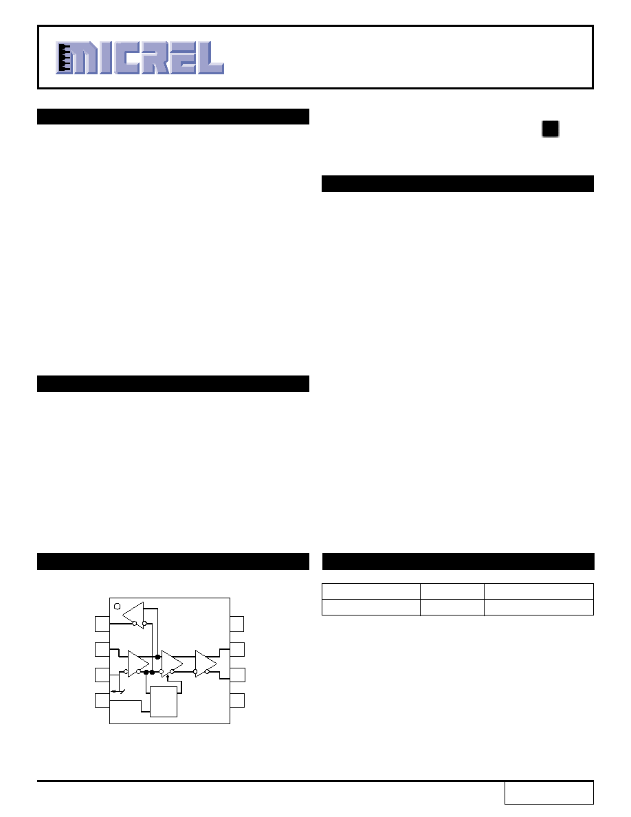
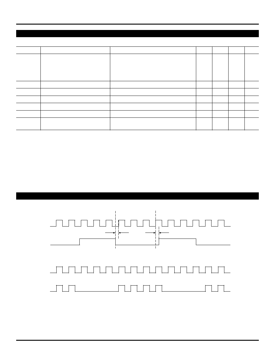
The SY89250V provides an /EN input which is synchro-
nized with the data input (D) signal in a way that provides
glitchless gating of the Q
HG
and /Q
HG
outputs. When the /EN
signal is LOW, the input is passed to the outputs and the data
output equals the data input. When the data input is HIGH and
the /EN goes HIGH, it will force the Q
HG
LOW and the /Q
HG
HIGH on the next negative transition of the data input. If the
data input is LOW when the /EN goes HIGH, the next data
transition to a HIGH is ignored and Q
HG
remains LOW and
/Q
HG
remains HIGH. The next positive transition of the data
input is not passed on to the data outputs under these
conditions. The Q
HG
and /Q
HG
outputs remain in their dis-
abled state as long as the /EN input is held HIGH. The /EN
input has no influence on the /Q output and the data input is
passed on (inverted) to this output whether /EN is HIGH or
LOW. This configuration is ideal for crystal oscillator applica-
tions, where the oscillator can be free running and gated on
and off synchronously without adding extra counts to the
output.
All support documentation can be found on Micrel's web
site at www.micrel.com.
DESCRIPTION
s
3.3V and 5V power supply options
s
250ps propagation delay
s
Very high voltage gain
s
Ideal for Pulse Amplifier and Limiting Amplifier
applications
s
Data synchronous Enable/Disable (/EN) on Q
HG
and
/Q
HG
provides for complete glitchless gating of the
outputs
s
Ideal for gating timing signals
s
Complete solution for high quality, high frequency
crystal oscillator applications
s
Available in an ultra-small 8-pin (2mm
◊◊
◊◊
◊
2mm)
MLFTM package
FEATURES
Precision EdgeTM
SY89250V
ENHANCED DIFFERENTIAL
RECEIVER
Rev.: A
Amendment: /0
Issue Date:
Oct. 2003
Precision EdgeTM
Precision Edge is a trademark of Micrel, Inc.
Micro
LeadFrame and MLF are trademarks of Amkor Technology, Inc.
Micrel Part Number
PECL/ECL
Functional Cross
SY89250V
100k
SY100EL16VC
FUNCTIONAL CROSS REFERENCE
APPLICATIONS
s
Oscillator modules
BLOCK DIAGRAM
1
2
3
4
5
6
8
LEN Q
D
V
BB
LATCH
OE
7
V
CC
Q
HG
/Q
HG
V
EE
/Q
D
V
BB
/EN
2
Precision EdgeTM
SY89250V
Micrel
PACKAGE/ORDERING INFORMATION
Ordering Information
Package PECL/ECL Operating
Package
Part Number
Type
Logic
Range
Marking
SY89250VMI
MLF-8
100KEL
Industrial
250
SY89250VMITR
(1)
MLF-8
100KEL
Industrial
250
Note:
1. Tape and Reel.
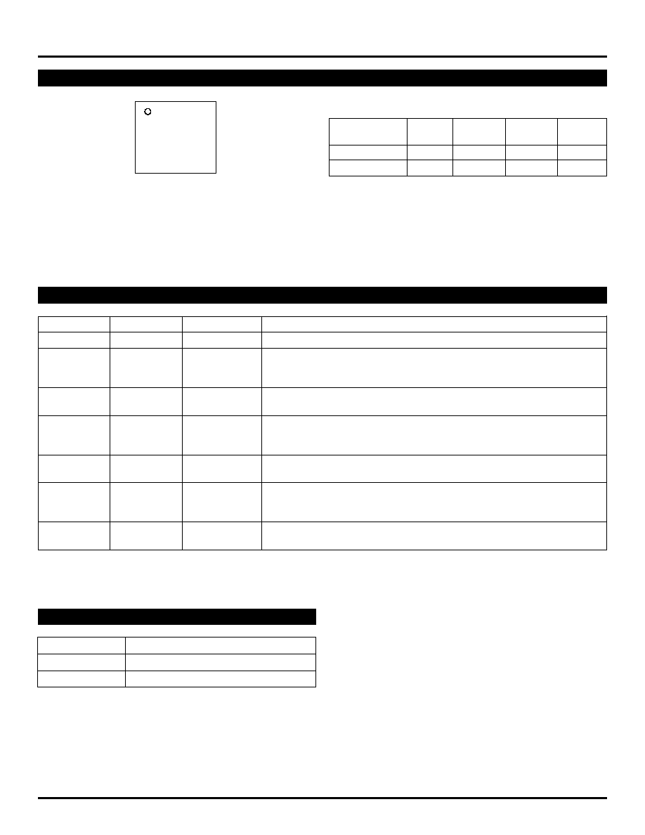
/Q
D
VBB
/EN
VCC
QHG
/QHG
VEE
1
2
3
4
8
7
6
5
8-Pin MLFTM
(Ultra-Small Outline)
/EN
Q
HG
Output
0
Data
1
Logic Low
TRUTH TABLE
PIN DESCRIPTION
Pin Number
Pin Name
Type
Pin Function
1
/Q
100k
Single-Ended PECL/ECL Feedback Output.
2
D
100k
Single-Ended PECL/ECL Input: The signal input includes an internal 75k
pull-down ECL Input resistor. If input is left open, Q output will default to
LOW. See "Input
Interface Applications"
section for single-ended inputs.
3
VBB
Reference
Bias Voltage: VCC≠1.3V. Used as reference voltage when AC-coupling to
Output Voltage
the D input. Max sink/source is
±
0.5mA.
4
/EN
Enable Input
/EN Input which is synchronized with data input (D) signal in a way that
provides glitchless gating of Q
HG
and /Q
HG
outputs. Includes internal 75k
pull-down resistor. Default is LOW
5
VEE,
Negative
Negative Power Supply: V
EE
and exposed pad must be tied to most
Exposed Pad
Power Supply
negative supply. For PECL/LVPECL connect to ground.
6, 7
/QHG, QHG
100k
Differential PECL/ECL Output: Defaults to LOW if D inputs left open.
ECL Output
See
"Output
Interface Applications"
section for recommendations on
terminations.
8
VCC
Positive
Positive Power Supply: Bypass with 0.1
µ
F//0.01
µ
F low ESR capacitors.
Power Supply
3
Precision EdgeTM
SY89250V
Micrel
Absolute Maximum Ratings
(1)
Power Supply Voltage (V
CC
) ....................... ≠0.5V to +6.0V
ECL Input Voltage (V
IN
) ............................ 0V to V
CC
+0.5V
Voltage Applied to Output at HIGH State
(V
OUT
) ........................................................ ≠0.5V to V
CC
Current Applied to Output at LOW State
(I
OUT
) .......................................... Twice the rated I
OL
mA
Lead Temperature (soldering, 10 sec.) ..................... 220
∞
C
Storage Temperature (T
S
) ....................... ≠65
∞
C to +150
∞
C
Operating Ratings
(2)
Power Supply Voltage
|
V
CC
≠V
EE
| ....
3.3V
±
10% or 5V
±
10%
Ambient Temperature (T
A
) ......................... ≠40
∞
C to +85
∞
C
Package Thermal Resistance,
(3)
MLFTM
(
JA
)
Still-Air ............................................................. 93
∞
C/W
MLFTM
(
JB
), ....................................................... 60
∞
C/W
T
A
= ≠40
∞
C to +85
∞
C; unless otherwise stated.
Symbol
Parameter
Condition
Min
Typ
Max
Units
V
EE
Power Supply
|
V
CC
≠V
EE
|
3.0
3.3
3.6
V
|
V
CC
≠V
EE
|
4.5
5.0
5.5
V
I
EE
Power Supply Current
46
mA
I
IH
Input HIGH Current
150
µ
A
V
BB
Output Reference Voltage
V
CC
≠1.38 V
CC
≠1.32 V
CC
≠1.26
V
DC ELECTRICAL CHARACTERISTICS
V
CC
= +3.3V
±
10% or +5V
±
10% and V
EE
= 0V; V
CC
= 0V and V
EE
= ≠3.3V
±
10% or ≠5V
±
10%; T
A
= ≠40
∞
C to +85
∞
C; unless otherwise stated.
Symbol
Parameter
Condition
Min
Typ
Max
Units
V
OH
Output HIGH Voltage
Note 4
V
CC
≠1.085
V
CC
≠0.880
V
V
OL
Output LOW Voltage
Note 4
V
CC
≠1.830
V
CC
≠1.555
V
V
IH
Input HIGH Voltage
V
CC
≠1.165
V
CC
≠0.880
V
V
IL
Input LOW Voltage
V
CC
≠1.810
V
CC
≠1.475
V
V
BB
Output Reference Voltage
V
CC
≠1.38
V
CC
≠1.26
V
V
PP
Minimum Input Swing
150
mV
I
IH
Input HIGH Current
150
µ
A
I
IL
Input LOW Current
0.5
µ
A
Notes:
1. Permanent device damage may occur if ABSOLUTE MAXIMUM RATINGS are exceeded. This is a stress rating only and functional operation is not
implied at conditions other than those detailed in the operational sections of this data sheet. Exposure to ABSOLUTE MAXIMUM RATlNG conditions
for extended periods may affect device reliability.
2. The data sheet limits are not guaranteed if the device is operated beyond the operating ratings.
3. Package thermal resistance assumes exposed pad is soldered (or equivalent) to the devices most negative potential on the PCB.
4. Output loaded with 50
to V
CC
≠2V.
DC ELECTRICAL CHARACTERISTICS
4
Precision EdgeTM
SY89250V
Micrel
V
EE
= V
EE
(min) to V
EE
(max); V
CC
= GND; T
A
= ≠40
∞
C to +85
∞
C; unless otherwise stated.
Symbol
Parameter
Condition
Min
Typ
Max
Units
t
pd
Propagation Delay to:
Q, /Q Output
D (Diff)
380
ps
D (SE)
430
ps
QHG, /QHG Output
D (Diff)
730
ps
D (SE)
780
ps
t
S
Set-Up Time
/EN
150
ps
t
H
Hold Time
/EN
150
ps
t
SKEW
Duty Cycle Skew
(Diff)
(5)
5
20
ps
V
PP
Minimum Input Swing
/EN
(6)
150
mV
V
CMR
Common Mode Range
/EN
(7)
≠1.3
≠0.4
V
t
r
, t
f
Output Q Rise/Fall Times
At full output swing
100
225
350
ps
(20% to 80%)
Notes:
5. Duty cycle skew is the difference between a t
pd
propagation delay through a device.
6. Minimum input swing for which AC parameters are guaranteed. The device has a DC gain of
40 to Q, /Q outputs and a DC gain of
200 or higher
to /Q
HG
, Q
HG
outputs.
7. The CMR range is referenced to the most positive side of the differential input signal. Normal operation is obtained if the HIGH level falls within the
specified range and the peak-to-peak voltage lies between V
PP
(min) and 1V. The lower end of the CMR range varies 1:1 with V
EE
. The numbers in
the spec table assume a nominal V
EE
= ≠3.3V. Note for PECL operation, the V
CMR
(min) will be fixed at 3.3V ≠ |V
CMR
(min)|.
AC ELECTRICAL CHARACTERISTICS
TIMING DIAGRAM
D
Q
Q
HG
/EN
t
S
t
H
5
Precision EdgeTM
SY89250V
Micrel
Part Number
Function
Data Sheet Link
SY89306/316V
3.3V/5V 2.5GHz PECL/ECL
www.micrel.com/product-info/products/sy89306-316v.shtml
Differential Receiver/Buffer
SY89206/216V
3.3V/5V 1GHz PECL/ECL
www.micrel.com/product-info/products/sy89206-216v.shtml
Differential Receiver/Buffer
HBW Solutions
New Products and Applications
www.micrel.com/product-info/products/solutions.shtml
RELATED PRODUCT AND SUPPORT DOCUMENTATION
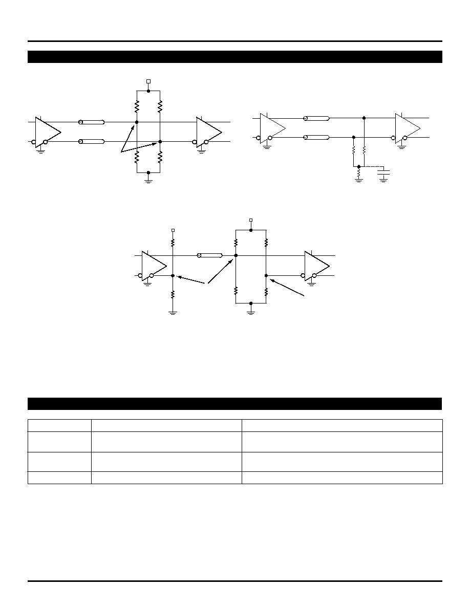
OUTPUT INTERFACE APPLICATIONS
Z
O
= 50
R2
R1
R1
R2
R3
R4
V
CC
--2V
V
CC
--1.3V
V
CC
V
CC
V
CC
V
CC
V
CC
= 3.3V; R1 = 130
, R2 = 82
, R3 = 1k
, R4 = 1.6k
,
V
CC
= 5V; R1 = 83
, R2 = 125
, R3 = 1k
, R4 = 2.8k
,
Figure 1c. Terminating Unused I/O
R2
R2
Z
O
= 50
Z
O
= 50
R1
R1
V
CC
--2V
V
CC
V
CC
V
CC
V
CC
= 3.3V; R1 = 130
, R2 = 82
V
CC
= 5V; R1 = 83
, R2 = 125
Figure 1a. Parallel Thevenin-Equivalent Termination
Z
O
= 50
Z
O
= 50
R
pd
50
50
C (Optional)
0.01
µ
F
V
CC
V
CC
V
CC
= 3.3V; Rpd = 50
V
CC
= 5V; Rpd = 100
Figure 1b. Three Resistor "Y Termination"