1
Precision Edge
Æ
SY89311U
Micrel, Inc.
M9999-072005
hbwhelp@micrel.com or (408) 955-1690
DESCRIPTION
s
2.5V, 3.3V and 5V power supply
s
Guaranteed AC parameters over temperature:
∑ f
MAX
> 3.0GHz
∑ < 20ps output-to-output skew
∑ < 200ps t
r
/ t
f
∑ < 300ps propagation delay
s
100K compatible I/O
s
Wide temperature range: ≠40
∞
C to +85
∞
C
s
Available in ultra-small 8-pin MLFTM
(2mm
◊◊
◊◊
◊
2mm) package
FEATURES
Precision Edge
Æ
SY89311U
Rev.: B
Amendment: /0
Issue Date:
July 2005
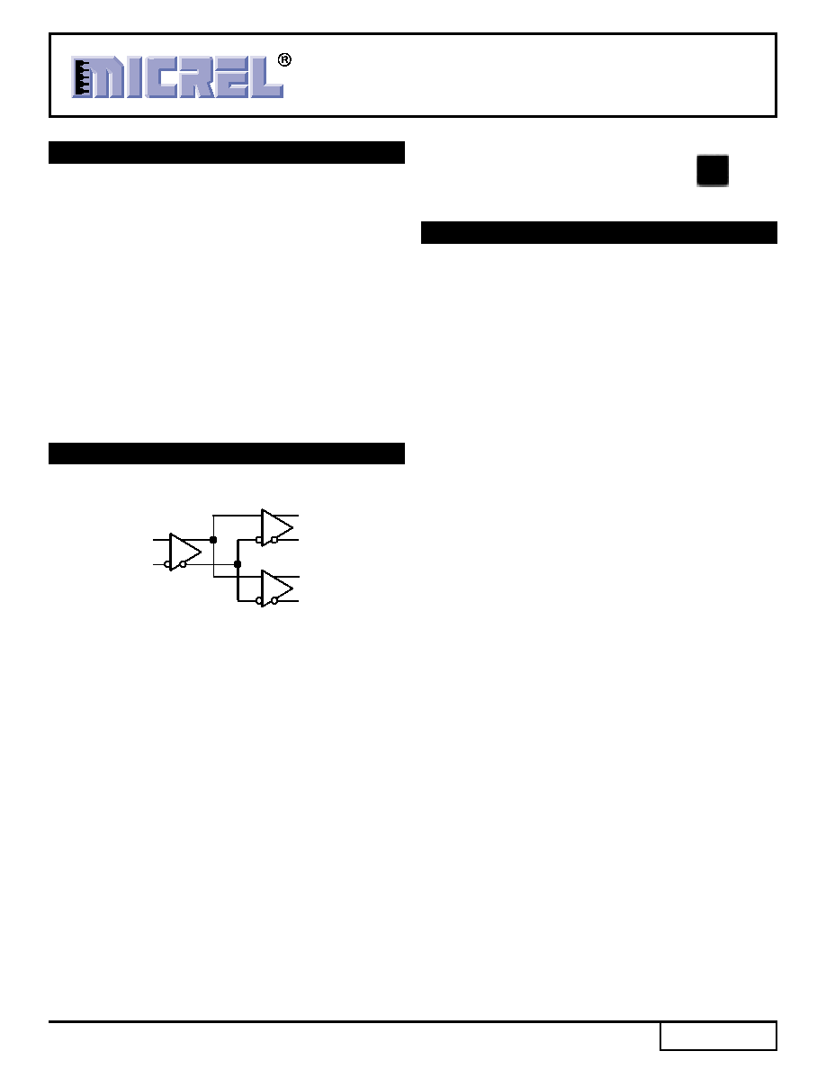
The SY89311U is a precision, high-speed 1:2 differential
fanout buffer. Having within-device skews and output
transition times significantly improved over the EL11V, the
SY89311U is ideally suited for those applications which
require the ultimate in AC performance in a small package.
The differential inputs of the SY89311U employ clamping
circuitry to maintain stability under open input conditions. If
the inputs are left open, the Q outputs will be LOW.
The differential inputs can accept 10/100K ECL/PECL
signals (external termination required) and the outputs are
100K ECL/PECL compatible.
Precision Edge
Æ
Precision Edge is a registered trademark of Micrel, Inc.
MicroLeadFrame and MLF are trademarks of Amkor Technology, Inc.
2.5V/3.3V/5V 1:2 DIFFERENTIAL
PECL/LVPECL/ECL FANOUT BUFFER
BLOCK DIAGRAM
Q0
/Q0
Q1
/Q1
IN
/IN
PECL
PECL
2
Precision Edge
Æ
SY89311U
Micrel, Inc.
M9999-072005
hbwhelp@micrel.com or (408) 955-1690
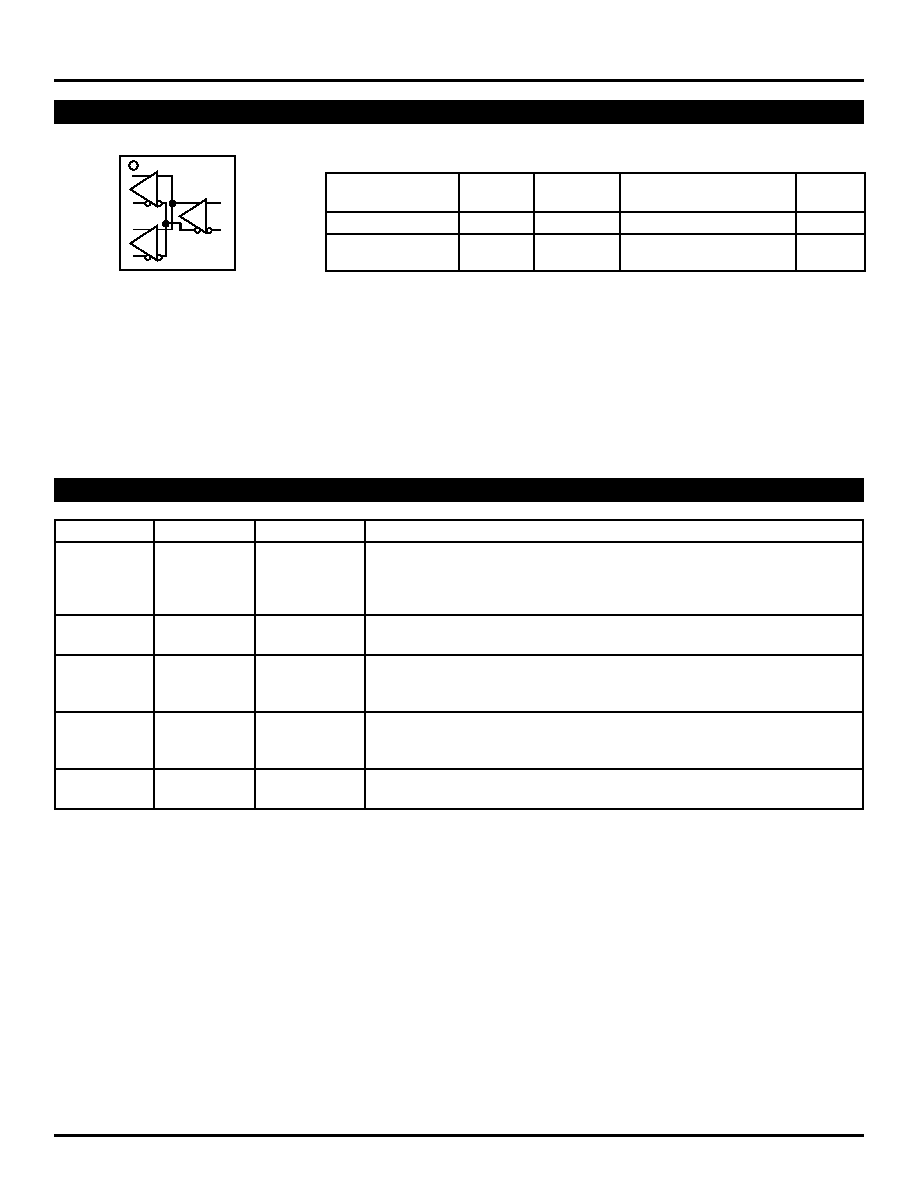
PIN DESCRIPTION
Pin Number
Pin Name
Type
Pin Function
1, 2, 3, 4
Q0, /Q0,
100K Output
Differential PECL/ECL Outputs: Default to LOW if IN inputs are left open.
Q1, /Q1
See"Output Interface Applications" section for recommendations on
terminations. Unused output pairs may be left floating without any inpact on
skew or jitter.
5
VEE,
Negative
Negative Power Supply: V
EE
and exposed pad must be tied to most negative
Exposed Pad
Power Supply
supply. For PECL/LVPECL connect to ground.
6
/IN
100K Input
Differential PECL/ECL Input: Internal 75k
pull-up and pull-down resistors.
If left floating, pin defaults to V
CC
/2. When not used, this input can be left
open. See "Input Interface Applications" section for single-ended inputs.
7
IN
100K Input
Differential PECL/ECL Input: Internal 75k
pull-down resistor. If left open,
pin defaults LOW. Q output will be LOW. Accepts differential 10K and 100K
ECL/PECL. See "Input Interface Applications" section for single-ended inputs.
8
VCC
Positive
Positive Power Supply: Bypass with 0.1
µ
F//0.01
µ
F low ESR capacitors.
Power Supply
PACKAGE/ORDERING INFORMATION
Q0
/Q0
Q1
/Q1
VCC
IN
/IN
VEE
1
2
3
4
8
7
6
5
8-Pin MLFTM
Ultra-Small Outline (2mm
◊◊
◊◊
◊
2mm)
Ordering Information
Package
Operating
Package
Lead
Part Number
Type
Range
Marking
Finish
SY89311UMITR
MLF-8
Industrial
HP11
Sn-Pb
SY89311UMGTR
MLF-8
Industrial
HP11 with
Pb-Free
Pb-Free bar-line indicator
NiPdAu
3
Precision Edge
Æ
SY89311U
Micrel, Inc.
M9999-072005
hbwhelp@micrel.com or (408) 955-1690
Absolute Maximum Ratings
(1)
Supply Voltage (V
CC
) .................................. ≠0.5V to +6.0V
Input Voltage (V
IN
) ......................................... ≠0.5V to V
CC
LVPECL Output Current (I
OUT
)
Continuous ............................................................. 50mA
Surge .................................................................... 100mA
Input Current
Source or sink current on IN, /IN ..........................
±
50mA
Lead Temperature (soldering, 20 sec.) ................... +260
∞
C
Storage Temperature (T
S
) ....................... ≠65
∞
C to +150
∞
C
Operating Ratings
(2)
Supply Voltage |V
CC
≠V
EE
| .................. +2.375V to +2.625V
............................................................ +3.0V to +3.6V
............................................................ +4.5V to +5.5V
Ambient Temperature (T
A
) ......................... ≠40
∞
C to +85
∞
C
Package Thermal Resistance, Note 3
MLFTM (
JA
)
Still-Air ................................................................. 93
∞
C/W
500lfpm ............................................................... 87
∞
C/W
MLFTM (
JB
)
Junction-to-Board ................................................ 60
∞
C/W
Symbol
Parameter
Condition
Min
Typ
Max
Units
V
CC
Power Supply Voltage
LVPECL
2.375
2.5
2.625
V
LVPECL
3.0
3.3
3.6
V
PECL
4.5
5.0
5.5
V
ECL
≠5.5
≠5.0
≠4.5
V
LVECL
≠3.6
≠3.3
≠3.0
V
LVECL
≠2.625
≠2.5
≠2.375
V
I
EE
Power Supply Current
Max. V
CC
, no load
30
44
mA
I
IH
Input HIGH Current
V
IN
= V
IH
150
µ
A
I
IL
Input LOW Current
IN
V
IN
= V
IL
0.5
µ
A
/IN
V
IN
= V
IL
≠150
µ
A
C
IN
Input Capacitance
1.0
pF
DC ELECTRICAL CHARACTERISTICS
(4)
T
A
= ≠40
∞
C to +85
∞
C
V
CC
= +2.5V
±
5% or +3.3V
±
10% or +5.0V
±
10% and V
EE
= 0V; V
CC
= 0V and V
EE
= ≠2.5V
±
5% or ≠3.3V
±
10% or ≠5.0V
±
10%;
R
L
= 50
to V
CC
≠2V; T
A
= ≠40
∞
C to +85
∞
C, unless otherwise noted.
Symbol
Parameter
Condition
Min
Typ
Max
Units
V
OH
Output HIGH Voltage
V
CC
≠1.145
V
CC
≠0.895
V
V
OL
Output LOW Voltage
V
CC
≠1.945
V
CC
≠1.695
V
V
IH
Input HIGH Voltage
V
CC
≠1.225
V
CC
≠0.88
V
V
IL
Input LOW Voltage
V
CC
≠1.945
V
CC
≠1.625
V
V
IHCMR
Input HIGH Voltage Common
Note 5
V
EE
+1.2
V
CC
V
Mode Range
I
IH
Input HIGH Current
V
IN =
V
IH
150
µ
A
I
IL
Input LOW Current (IN)
V
IN =
V
IL
0.5
µ
A
Input LOW Current (/IN)
V
IN =
V
IL
≠150
µ
A
Notes:
1. Permanent device damage may occur if ABSOLUTE MAXIMUM RATINGS are exceeded. This is a stress rating only and functional operation is not
implied at conditions other than those detailed in the operational sections of this data sheet. Exposure to ABSOLUTE MAXIMUM RATlNG conditions
for extended periods may affect device reliability.
2. The data sheet limits are not guaranteed if the device is operated beyond the operating ratings.
3. Package Thermal Resistance values assume exposed pad is soldered (or equivalent) to the device's most negative potential on the PCB.
4. This circuit is designed to meet the DC specifications shown in the above table after thermal equilibrium has been established.
5. V
IHCMR
(min) varies 1:1 with V
EE
, (max) varies 1:1 with V
CC
.
(100K) ECL/LVECL DC ELECTRICAL CHARACTERISTICS
4
Precision Edge
Æ
SY89311U
Micrel, Inc.
M9999-072005
hbwhelp@micrel.com or (408) 955-1690
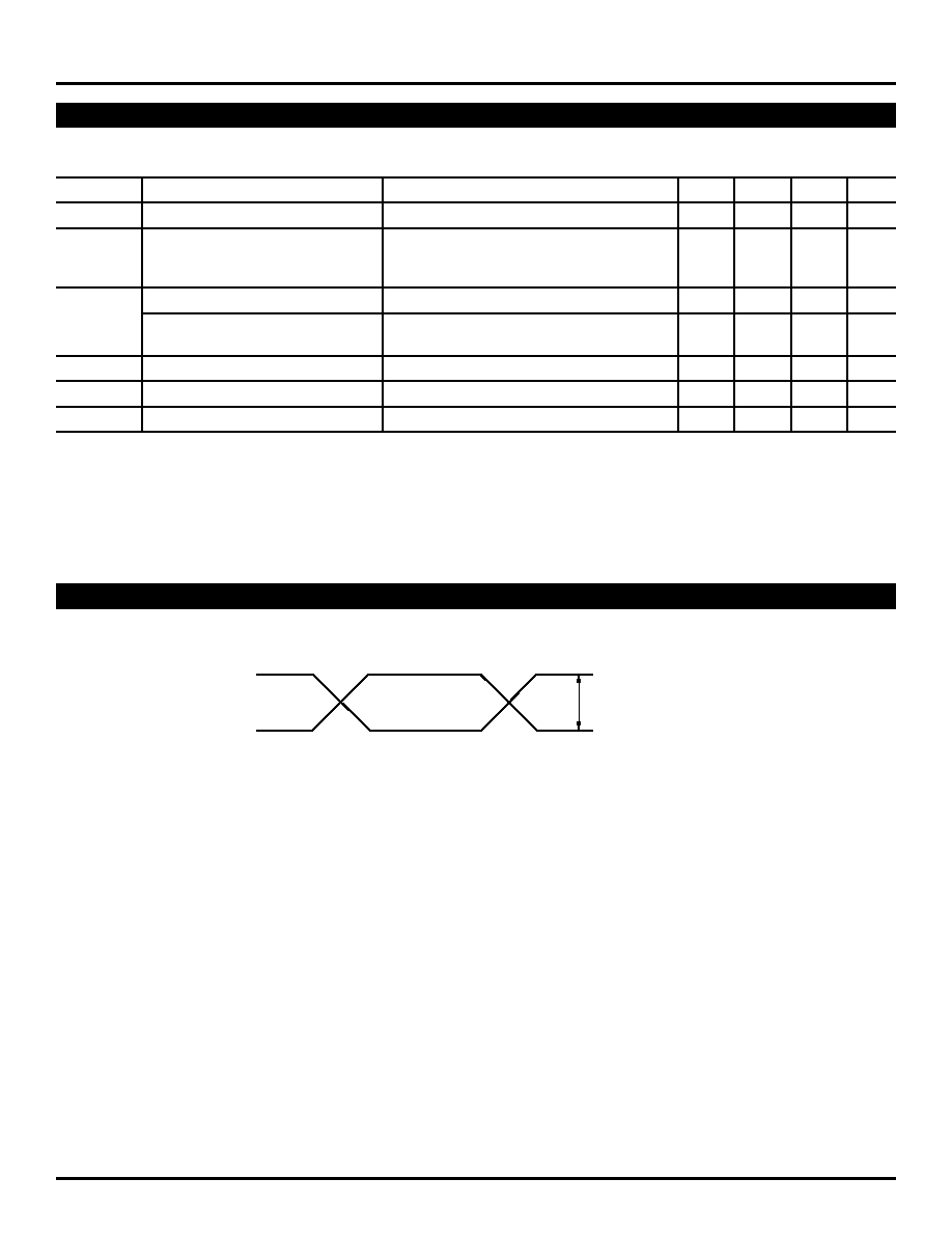
INPUT WAVEFORM
IN
V
IHCMR
/IN
V
DIFF
= 150mV to 1200mV
V
CC
= +2.5V
±
5% or +3.3V
±
10% or +5.0V
±
10% and V
EE
= 0V; V
CC
= 0V and V
EE
= ≠2.5V
±
5% or ≠3.3V
±
10% or or ≠5.0V
±
10%;
R
L
= 50
to V
CC
≠2V; T
A
= ≠40
∞
C to +85
∞
C, unless otherwise noted.
Symbol
Parameter
Condition
Min
Typ
Max
Units
f
MAX
Maximum Toggle Frequency
3
GHz
t
pd
Propagation Delay (Differential)
IN to Q, /Q
V
CC
= 3.3V/5V
140
220
300
ps
IN to Q, /Q
V
CC
= 2.5V
170
240
360
ps
t
SKEW
Within-Device Skew
Q, /Q
Note 7
5
20
ps
Part-to-Part Skew
V
CC
= 3.3V/5V, Note 7
150
ps
V
CC
= 2.5V, Note 7
120
ps
t
JITTER
Cycle-to-Cycle Jitter (rms)
1
ps
(rms)
V
DIFF
Input Swing
Note 8
150
800
1200
mV
t
r,
t
f
Output Rise/Fall Time (20% to 80%)
70
120
200
ps
Notes:
6. Measured with 750mV input signal, 50% duty cycle. V
DIFF_OUT
is
400mV.
7. Skew is measured between outputs under identical transitions. Duty cycle skew is defined only for differential operation when the delays are
measured from the cross point of the inputs to the cross point of the outputs.
8. See "Input Waveform."
AC ELECTRICAL CHARACTERISTICS
(6)
5
Precision Edge
Æ
SY89311U
Micrel, Inc.
M9999-072005
hbwhelp@micrel.com or (408) 955-1690
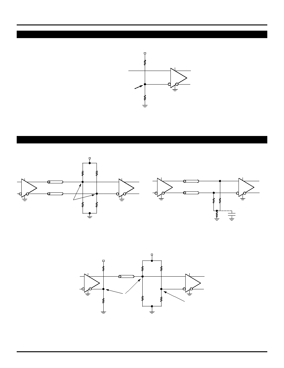
INPUT INTERFACE APPLICATIONS
IN
V
CC
V
CC
--1.3V
V
CC
= 2.5V; R1 = 1k
, R2 = 900
V
CC
= 3.3V; R1 = 1k
, R2 = 1.6k
V
CC
= 5V; R1 = 1k
, R2 = 2.8k
V
CC
R1
R2
Figure 1. Single-Ended Input
(Terminating unused input)
LVPECL OUTPUT INTERFACE APPLICATIONS
Z
O
= 50
R2
R1
R1
R2
R3
R4
V
CC
--2V
V
CC
--1.3V
V
CC
V
CC
V
CC
V
CC
V
CC
= 2.5V; R1 = 250
, R2 = 62.5
, R3 = 1k
, R4 = 900
,
V
CC
= 3.3V; R1 = 130
, R2 = 82
, R3 = 1k
, R4 = 1.6k
,
V
CC
= 5V; R1 = 83
, R2 = 125
, R3 = 1k
, R4 = 2.8k
,
Figure 2c. Terminating Unused I/O
R2
R2
Z
O
= 50
Z
O
= 50
R1
R1
V
CC
--2V
V
CC
V
CC
V
CC
V
CC
= 2.5V; R1 = 250
, R2 = 62.5
V
CC
= 3.3V; R1 = 130
, R2 = 82
V
CC
= 5V; R1 = 83
, R2 = 125
Figure 2a. Parallel Thevenin-Equivalent
Termination
Z
O
= 50
Z
O
= 50
R
pd
50
50
C (Optional)
0.01
µ
F
V
CC
V
CC
V
CC
= 2.5V; Rpd = 39
V
CC
= 3.3V; Rpd = 50
V
CC
= 5V; Rpd = 100
Figure 2b. Three Resistor
"Y Termination"
6
Precision Edge
Æ
SY89311U
Micrel, Inc.
M9999-072005
hbwhelp@micrel.com or (408) 955-1690
MICREL, INC.
2180 FORTUNE DRIVE
SAN JOSE, CA 95131
USA
TEL
+ 1 (408) 944-0800
FAX
+ 1 (408) 474-1000
WEB
http://www.micrel.com
The information furnished by Micrel in this datasheet is believed to be accurate and reliable. However, no responsibility is assumed by Micrel for its use.
Micrel reserves the right to change circuitry and specifications at any time without notification to the customer.
Micrel Products are not designed or authorized for use as components in life support appliances, devices or systems where malfunction of a product can
reasonably be expected to result in personal injury. Life support devices or systems are devices or systems that (a) are intended for surgical implant into
the body or (b) support or sustain life, and whose failure to perform can be reasonably expected to result in a significant injury to the user. A Purchaser's
use or sale of Micrel Products for use in life support appliances, devices or systems is at Purchaser's own risk and Purchaser agrees to fully indemnify
Micrel for any damages resulting from such use or sale.
© 2005 Micrel, Incorporated.
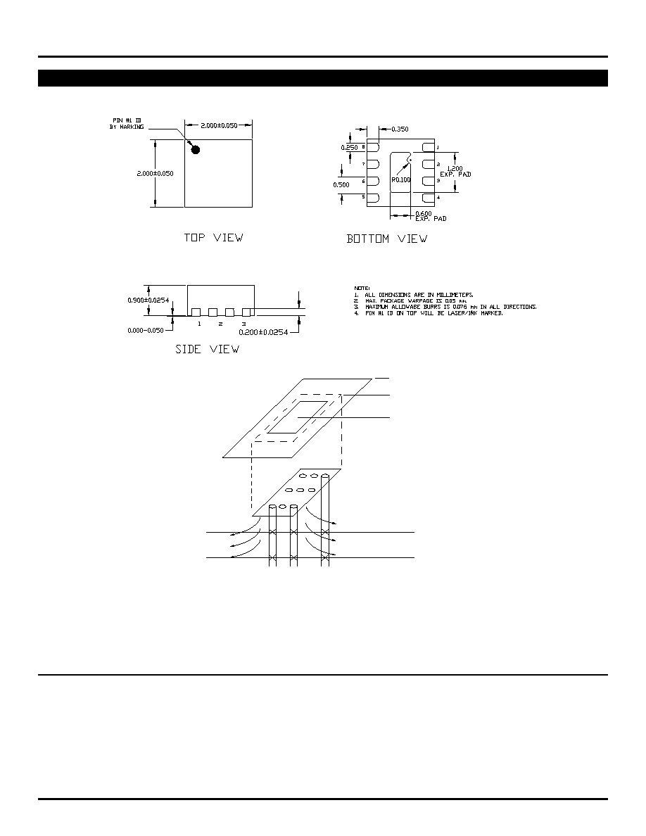
8 LEAD ULTRA-SMALL EPAD-
MicroLeadFrameTM (MLF-8)
Package
EP- Exposed Pad
Die
CompSide Island
Heat Dissipation
Heavy Copper Plane
Heavy Copper Plane
V
EE
V
EE
Heat Dissipation
PCB Thermal Consideration for 8-Pin MLFTM Package
Package Notes:
1. Package meets Level 2 qualification.
2. All parts are dry-packaged before shipment.
3. Exposed pads must be soldered to a ground for proper thermal management.