1
Precision EdgeTM
SY89312V
Micrel
DESCRIPTION
s
Guaranteed AC performance over temperature and
voltage
∑ > 4GHz f
MAX
input
∑ < 160ps t
r
/t
f
∑ < 440ps t
pd
s
3.3V and 5V power supply operation
s
100k ECL/PECL compatible I/O
s
Internal 75K
input pull-down resistors
s
Wide operating temperature range: ≠40
∞
C to +85
∞
C
s
Available in ultra-small 8-pin MLFTM
(2mm x 2mm)
package
FEATURES
Precision EdgeTM
SY89312V
Rev.: A
Amendment: /0
Issue Date:
June 2003
The SY89312V is an integrated
˜
2 divider with differential
clock inputs. It is functionally equivalent to the SY100EP32V
but in an ultra-small 8-lead MLFTM package that features a
70% smaller footprint.
The V
BB
pin, an internally generated voltage supply, is
available for this device only. For single-ended input
conditions, the unused differential input is connected to VBB
as a switching reference voltage. V
BB
may also bias
AC-coupled inputs. When used, decouple V
BB
and V
CC
via
a 0.01
µ
F capacitor and limit current sourcing or sinking to
0.5mA. When not used, V
BB
should be left open.
The reset pin is asynchronous and is asserted when it is
high. Upon power-up, the internal flip-flops will be in a
random state; the reset allows for the synchronous use of
multiple SY89312Vs in a system.
Precision EdgeTM
Precision Edge is a trademark of Micrel, Inc.
Micro
LeadFrame and MLF are trademarks of Amkor Technology, Inc.
3.3V/5V, 4GHz PECL/ECL
˜
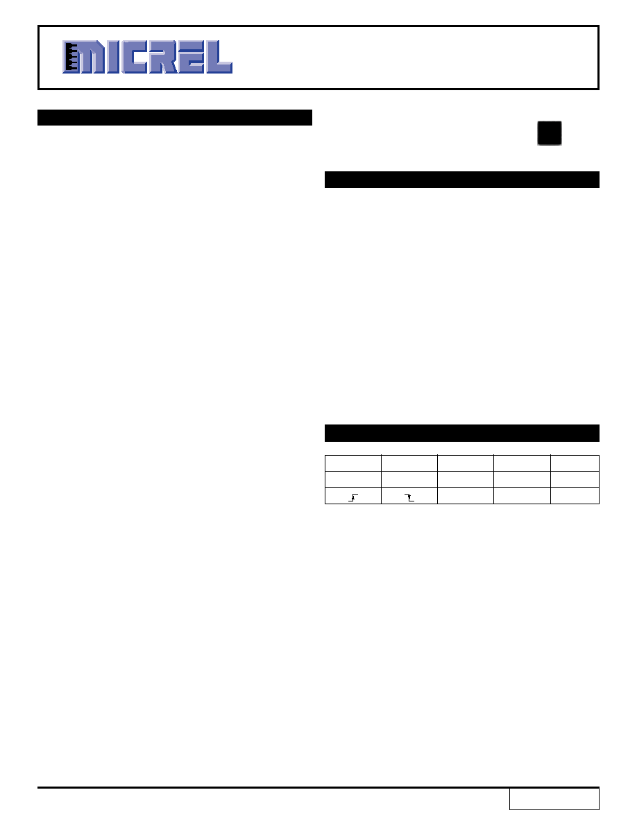
2 CLOCK GENERATOR
CLK
/CLK
RESET
Q
/Q
X
X
H
L
H
L
F
F
TRUTH TABLE
(Note 1)
Note 1.
F = Divide by 2 function
2
Precision EdgeTM
SY89312V
Micrel
PACKAGE/ORDERING INFORMATION
Ordering Information
Package
Operating
Package
Part Number
Type
Range
Marking
SY89312VMITR*
MLF-8
Industrial
312
*Tape and Reel
PIN DESCRIPTION
Pin Number
Pin Name
Type
Pin Function
2, 3
CLK, /CLK
100k ECL/PECL
Differential PECL/ECL Input: Internal 75k
pull-down resistor. If left open,
Input
pin defaults LOW. See
"Input Interface Applications"
section for single-
ended inputs.
7, 6
Q, /Q
100k ECL/PECL
Differential PECL/ECL Output: Output CLK input divided by 2. See
"Output
Output
Interface Applications"
section for recommendations on terminations.
8
VCC
Positive
Positive Power Supply: Bypass with 0.1
µ
F//0.01
µ
F low ESR capacitors.
Power Supply
5
VEE,
Negative
Negative Power Supply: V
EE
and Exposed pad must be tied to most
Exposed Pad
Power Supply
negative supply. For PECL/LVPECL connect to ground.
4
VBB
Reference
Bias Reference Voltage: VCC≠1.4V. Used as reference voltage for single-
Voltage Output
ended inputs or AC-coupling to the CLK, /CLK inputs. Max sink/source is
±
0.5mA. See
"Input Interface Applications"
section.
1
Reset
100k ECL/PECL
Single-ended Input: PECL/ECL Asynchronous reset.
Input
RESET
CLK
˜
2
R
/CLK
VBB
VCC
Q
/Q
VEE
1
2
3
4
8
7
6
5
TOP VIEW
8-Pin MLFTM
Ultra-Small Outline (2mm x 2mm)
3
Precision EdgeTM
SY89312V
Micrel
Absolute Maximum Ratings
(Note 1)
Supply Voltage (|V
CC
≠V
EE
|) ......................................... 6.0V
Input Voltage (V
IN
) ......................................... ≠0.5V to V
CC
LVPECL Output Current (I
OUT
)
Continuous ............................................................. 50mA
Surge .................................................................... 100mA
Current (V
BB
)
Source or sink current on V
BB
, Note 3 ................
±
1.5mA
Lead Temperature (soldering, 10 sec.) ................... +220
∞
C
Storage Temperature (T
S
) ....................... ≠65
∞
C to +150
∞
C
Operating Ratings
(Note 2)
Supply Voltage (|V
CC
≠V
EE
|) ............................ 3.0V to 3.6V
................................................................ 4.5V to 5.5V
Ambient Temperature (T
A
) ......................... ≠40
∞
C to +85
∞
C
Package Thermal Resistance (Note 4)
MLFTM (
JA
)
Still-Air ................................................................. 93
∞
C/W
500lfpm ............................................................... 87
∞
C/W
MLFTM (
JB
)
Junction-to-Board ................................................ 56
∞
C/W
V
CC
= +3.3V
±
10% or +5V
±
10% and V
EE
= 0V; V
CC
= 0V and V
EE
= ≠3.3V
±
10% or ≠5V
±
10%; R
L
= 50
to V
CC
≠2V; T
A
= ≠40
∞
C to +85
∞
C
unless otherwise stated.
Symbol
Parameter
Condition
Min
Typ
Max
Units
I
EE
Power Supply Current
Max V
CC
, no load
--
30
42
mA
V
OH
Output HIGH Voltage
V
CC
≠1.145
--
V
CC
≠0.895
V
V
OL
Output LOW Voltage
V
CC
≠1.945
--
V
CC
≠1.695
V
V
IH
Input HIGH Voltage
V
CC
≠1.225
--
V
CC
≠0.88
V
V
IL
Input LOW Voltage
V
CC
≠1.945
--
V
CC
≠1.625
V
V
IHCMR
Input HIGH Voltage
Note 5
V
EE
+2.0
--
V
CC
V
Common Mode Range
V
BB
Bias Voltage
V
CC
≠1.525 V
CC
≠1.425 V
CC
≠1.325
V
I
IH
Input HIGH Current
--
--
150
µ
A
I
IL
Input LOW Current CLK
0.5
--
--
µ
A
Input LOW Current /CLK
≠150
--
--
µ
A
Note 1.
Permanent device damage may occur if ABSOLUTE MAXIMUM RATINGS are exceeded. This is a stress rating only and functional operation
is not implied at conditions other than those detailed in the operational sections of this data sheet. Exposure to ABSOLUTE MAXIMUM
RATlNG conditions for extended periods may affect device reliability.
Note 2.
The data sheet limits are not guaranteed if the device is operated beyond the operating ratings.
Note 3.
Due to the limited drive capability use for input of the same package only.
Note 4.
Package thermal resistance assumes exposed pad is soldered (or equivalent) to the devices most negative potential on the PCB.
Note 5.
V
IHCMR
(min) varies 1:1 with V
EE
, (max) varies 1:1 with V
CC
.
PECL/ECL (100K) DC ELECTRICAL CHARACTERISTICS
4
Precision EdgeTM
SY89312V
Micrel
TIMING DIAGRAM
Q
CLK
t
RR
RESET
PECL: V
CC
= +3.3V
±
10% or +5V
±
10% and V
EE
= GND; ECL: V
EE
= ≠3.3V
±
10% or ≠5V
±
10% and V
CC
= GND; R
L
= 50
to V
CC
≠2V;
T
A
= ≠40
∞
C to +85
∞
C unless otherwise stated.
Symbol
Parameter
Condition
Min
Typ
Max
Units
f
MAX
Maximum Input Frequency
4
--
--
GHz
t
pd
Propagation Delay to Output
ps
Differential
RESET, CLK
Q, /Q
250
275
440
t
RR
Set/Reset Recovery
200
100
--
ps
t
PW
Minimum Pulse Width
RESET
550
200
--
ps
t
JITTER
Cycle-to-Cycle RMS Jitter
--
--
1
ps(rms)
V
PP
Input Voltage Swing
150
800
1200
mV
(Differential)
t
r
Output Rise/Fall Times
Q, /Q
50
100
160
ps
t
f
(20% to 80%)
Note 1.
Measured using a 750mV source, 50% duty cycle clock source.
AC ELECTRICAL CHARACTERISTICS
(Note 1)

5
Precision EdgeTM
SY89312V
Micrel
INPUT INTERFACE APPLICATIONS
Single-Ended
CLK
/CLK
SY89312V
0.01
µ
F
V
BB
V
CC
Figure 1. Single-Ended LVPECL Input
(Terminating Unused Input)
LVPECL OUTPUT INTERFACE APPLICATIONS
Z
O
= 50
R2
R1
R1
R2
R3
R4
V
CC
--2V
V
CC
--1.3V
V
CC
V
CC
V
CC
V
CC
V
CC
= 3.3V; R1 = 130
, R2 = 82
, R3 = 1k
, R4 = 1.6k
,
V
CC
= 5V; R1 = 83
, R2 = 125
, R3 = 1k
, R4 = 2.8k
,
Figure 2c. Terminating Unused I/O
R2
R2
Z
O
= 50
Z
O
= 50
R1
R1
V
CC
--2V
V
CC
V
CC
V
CC
V
CC
= 3.3V; R1 = 130
, R2 = 82
V
CC
= 5V; R1 = 83
, R2 = 125
Figure 2a. Parallel Thevenin-Equivalent
Termination
Z
O
= 50
Z
O
= 50
R
pd
50
50
C (Optional)
0.01
µ
F
V
CC
V
CC
V
CC
= 3.3V; Rpd = 50
V
CC
= 5V; Rpd = 100
Figure 2b. Three Resistor
"Y Termination"

6
Precision EdgeTM
SY89312V
Micrel
MICREL, INC.
1849 FORTUNE DRIVE
SAN JOSE, CA 95131
USA
TEL
+ 1 (408) 944-0800
FAX
+ 1 (408) 944-0970
WEB
http://www.micrel.com
The information furnished by Micrel in this datasheet is believed to be accurate and reliable. However, no responsibility is assumed by Micrel for its use.
Micrel reserves the right to change circuitry and specifications at any time without notification to the customer.
Micrel Products are not designed or authorized for use as components in life support appliances, devices or systems where malfunction of a product can
reasonably be expected to result in personal injury. Life support devices or systems are devices or systems that (a) are intended for surgical implant into
the body or (b) support or sustain life, and whose failure to perform can be reasonably expected to result in a significant injury to the user. A Purchaser's
use or sale of Micrel Products for use in life support appliances, devices or systems is at Purchaser's own risk and Purchaser agrees to fully indemnify
Micrel for any damages resulting from such use or sale.
© 2003 Micrel, Incorporated.
8 LEAD ULTRA-SMALL EPAD-
MicroLeadFrameTM (MLF-8)
Package
EP- Exposed Pad
Die
CompSide Island
Heat Dissipation
Heavy Copper Plane
Heavy Copper Plane
V
EE
V
EE
Heat Dissipation
PCB Thermal Consideration for 8-Pin MLFTM Package
Package Notes:
Note 1.
Package meets Level 2 qualification.
Note 2.
All parts are dry-packaged before shipment.
Note 3.
Exposed pads must be soldered to the most negative plane, equivalent to device V
EE
, for proper
thermal management.