1
Precision Edge
ģ
SY89327L
Micrel, Inc.
M9999-072005
hbwhelp@micrel.com or (408) 955-1690
DESCRIPTION
s
Input accepts virtually all logic standards:
∑ Single-ended: SSTL, TTL, CMOS
∑ Differential: LVDS, HSTL, CML
s
Guaranteed AC performance over temp and voltage:
∑ DC-to >2.5Gbps data rate throughput
∑ DC-to >2.5GHz clock f
MAX
∑ < 400ps In-to-Out t
pd
∑ < 200ps t
r
/t
f
s
Ultra-low jitter design:
∑ <1ps
RMS
random jitter
∑ <10ps
PP
deterministic jitter
∑ <1ps
RMS
cycle-to-cycle jitter
∑ <10ps
PP
total jitter (clock)
s
Low power: 46mW (typ)
s
100k LVPECL output
s
Flow-through pinout and fully differential design
s
Power supply 3.3V
Ī
10%
s
≠40
į
C to +85
į
C temperature range
s
Available in ultra-small 8-lead 2mm
◊◊
◊◊
◊
2mm MLFTM
package
FEATURES
3.3V 2.5Gbps
ANY INPUT-to-LVPECL
DIFFERENTIAL TRANSLATOR
Precision Edge
ģ
SY89327L
APPLICATIONS
s
High-speed logic
s
Data communications systems
s
Wireless communications systems
s
Telecom systems
Rev.: B
Amendment: /0
Issue Date:
July 2005
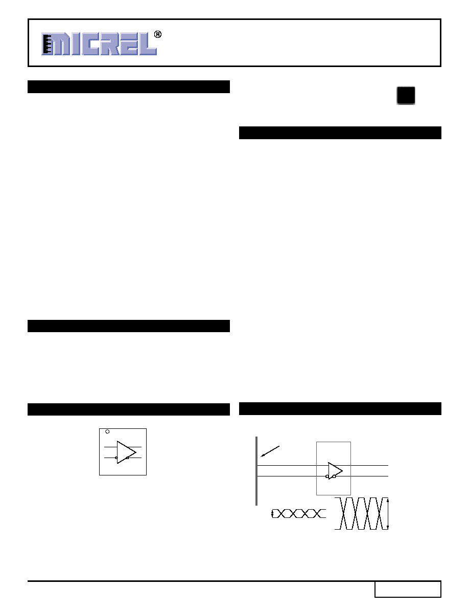
The SY89327L is a fully differential, high-speed translator
optimized to accept any logic standard from single-ended
TTL/CMOS to differential LVDS, HSTL, or CML and translate
it to LVPECL. Translation is guaranteed for speeds up to
2.5Gbps (2.5GHz toggle frequency). The SY89327L does
not internally terminate its inputs because different interfacing
standards have different termination requirements.
The SY89327L is a member of Micrel's Precision Edge
ģ
family of high-speed logic devices. This family features ultra-
small packaging, as well as high signal integrity and
operation at many different supply voltages.
All support documentation can be found on Micrel's web
site at www.micrel.com.
TYPICAL APPLICATIONS CIRCUIT
FUNCTIONAL BLOCK DIAGRAM
Precision Edge
ģ
NC
ANY IN
IN
/IN
NC
VCC
LVPECL OUT
Q
/Q
VEE
1
2
3
4
8
7
6
5
8-Lead MLFTM (2mm
◊◊
◊◊
◊
2mm)
100mV Input Swing
100mV
Input Waveform
Output Waveform
SY89327L
Backplane
800mV Output Swing (LVPECL)
800mV
LVPECL
Precision Edge is a registered trademark of Micrel, Inc.
MicroLeadFrame and MLF are trademarks of Amkor Technology, Inc.
2
Precision Edgeģ
SY89327L
Micrel, Inc.
M9999-072005
hbwhelp@micrel.com or (408) 955-1690
PACKAGE/ORDERING INFORMATION
Pin Number
Pin Name
Pin Function
2, 3
IN, /IN
Differential inputs: This input is the differential signal input to the device. This input
accepts AC- or DC-coupled signals as small as 100mV. External termination is required.
Please refer to the "Input Interface Applications" section for more details.
8
VCC
Positive power supply. Bypass with 0.1
Ķ
F
0.01
Ķ
F low ESR capacitors.
7, 6
Q, /Q
Differential LVPECL Output: Terminate with 50
to V
CC
≠2V. See "Output Interface
Applications" section. Output pair is 100k temperature compensated LVPECL compatible.
5
GND,
Ground: Ground pin and exposed pad must be connected to the same ground plane.
Exposed Pad
1, 4
NC
No connect.
PIN DESCRIPTION
NC
IN
/IN
NC
VCC
Q
/Q
GND
1
2
3
4
8
7
6
5
8-Lead MLFTM
FUNCTIONAL DESCRIPTION
Establishing Static Logic Inputs
Do not leave unused inputs floating. Tie either the true or
complement input to ground. A logic zero is achieved by
connecting the complement input to ground with the true
input floating. For a TTL input, tie a 2.5k
resistor between
the complement input and ground. See "Input Interface"
section.
Input Levels
LVDS, CML, and HSTL differential signals may be
connected directly to the D inputs. Depending on the actual
worst case voltage seen, the SY8327L's performance varies
as per the following table:
Input Voltage
Minimum
Maximum
Range
Voltage Swing
Translation Speed
0 to 2.4V
100mV
2.5Gbps
0 to V
CC
+0.3V
200mV
1.25Gbps
For LVDS applications, only point-to-point interfaces are
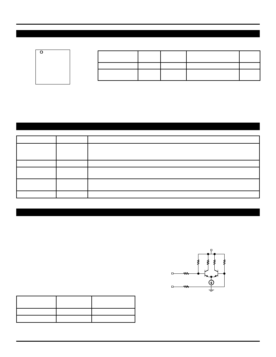
supported. Due to the current required by the input structure
shown in Figure 1, multi-drop and multi-point architectures
are not supported.
R2
1.5k
R2
1.5k
R1
1.05k
R1
1.05k
GND
D
IN
/D
IN
V
CC
Figure 1. Simplified Input Structure
Ordering Information
Package
Operating
Package
Lead
Part Number
Type
Range
Marking
Finish
SY89327LMITR
MLF-8
Industrial
327
Sn-Pb
SY89325LMGTR
MLF-8
Industrial
327 with
Pb-Free
Pb-Free bar-line indicator
NiPdAu
3
Precision Edge
ģ
SY89327L
Micrel, Inc.
M9999-072005
hbwhelp@micrel.com or (408) 955-1690
Absolute Maximum Ratings
(1)
Supply Voltage (V
CC
) ................................ ≠-0.5V to + 4.0V
Input Voltage (VIN) ......................................... ≠0.5V to V
CC
Input Current
Source or sink current on IN, /IN ..........................
Ī
50mA
Lead Temperature (soldering, 20 sec.) ................... +260
į
C
Storage Temperature (T
S
) ...................... ≠65
į
C to +150
į
C
Operating Ratings
(2)
Supply Voltage (V
CC
) ..................................... 3.0V to 3.6V
Ambient Temperature (T
A
) ......................... ≠40
į
C to +85
į
C
Package Thermal Resistance
(3)
MLFTM (
JA
)
Still-Air ................................................................. 93
į
C/W
500lfpm ............................................................... 87
į
C/W
MLFTM (
JB
)
Junction-to-Board ............................................... 32
į
C/W
T
A
= ≠40
į
C to +85
į
C; unless stated.
Symbol
Parameter
Condition
Min
Typ
Max
Units
V
CC
Power Supply
3.0
3.3
3.6
V
I
CC
Power Supply Current
No load, max. V
CC
(5)
28
45
mA
DC ELECTRICAL CHARACTERISTICS
(4)
V
CC
= 3.3V
Ī
10%; T
A
= ≠40
į
C to +85
į
C; R
L
= 50
to V
CC
≠2V, or equivalent, unless otherwise stated.
Symbol
Parameter
Condition
Min
Typ
Max
Units
V
OL
Output HIGH Voltage
V
CC
≠1.945
V
CC
≠1.695
V
Q, /Q
V
OH
Output Common Mode Range
V
CC
≠1.145
V
CC
≠0.895
V
Q, /Q
V
OUT
Output Voltage Swing
See Figure 2a
550
800
mV
Q, /Q
V
DIFF-OUT
Differential Output Voltage Swing
See Figure 2b
1100
1600
mV
PP
Q, /Q
Notes:
1. Permanent device damage may occur if the "Absolute Maximum Ratings" are exceeded. This is a stress rating only and functional operation is not
implied at conditions other than those detailed in the operational sections of this data sheet. Exposure to the
absolute maximum ratings conditions
for extended periods may affect device reliability.
2. The data sheet limits are not guaranteed if the device is operated beyond the operating ratings.
3. Package Thermal Resistance assumes exposed pad is soldered (or equivalent) to the devices' most negative potential on the PCB.
JB
uses 4-layer
JA
in still-air unless otherwise stated.
4. The circuit is designed to meet the DC specifications shown in the above table after thermal equilibrium has been established.
LVPECL OUTPUT DC ELECTRICAL CHARACTERISTICS
(4)
V
CC
= 3.3V
Ī
10%; T
A
= ≠40
į
C to +85
į
C; R
L
= 50
to V
CC
≠2V, or equivalent, unless otherwise stated.
Symbol
Parameter
Condition
Min
Typ
Max
Units
V
IH
Input HIGH Voltage
V
IH
min must be
1.2V
V
CC
+0.3
V
V
IL
Input LOW Voltage
≠0.3
V
V
IN
Input Voltage Swing
See Figure 2a, V
IH
< 2.4V
100
mV
See Figure 2a, V
IH
< V
CC
+0.3V
200
mV
INPUT ELECTRICAL CHARACTERISTICS
(4)
4
Precision Edgeģ
SY89327L
Micrel, Inc.
M9999-072005
hbwhelp@micrel.com or (408) 955-1690
V
CC
= 3.3V
Ī
10%; T
A
= ≠40
į
C to +85
į
C; R
L
= 50
to V
CC
≠2V, or equivalent, unless otherwise stated.
Symbol
Parameter
Condition
Min
Typ
Max
Units
f
MAX
Maximum Operating Frequency
NRZ Data
2.5
Gbps
V
OUT
200mV
Clock
2.5
GHz
t
pd
Propagation Delay
IN-to-Q, /IN-to-/Q
V
IN
100mV
400
ps
t
JITTER
Random Jitter (RJ)
Note 6
1
ps
RMS
Deterministic Jitter (DJ)
Note 7
10
ps
PP
Total Jitter (TJ)
Note 8
10
ps
PP
t
r
, t
f
Rise / Fall Time (20% to 80%)
At full output swing
200
ps
Q, /Q
Notes:
5. See "Timing Diagrams" section for definition of parameters. High frequency AC-parameters are guaranteed by design and characterization.
6. RJ is measured with a K28.7 comma detect character pattern, measured at f
MAX
.
7. DJ is measured at 2.5Gbps, with both K28.5 and 2
23
≠1 PRBS pattern.
8. Total jitter definition: with an ideal clock input of frequency
f
MAX
, no more than one output edge in 10
12
output edges will deviate by more than the
specified peak-to-peak jitter value.
AC ELECTRICAL CHARACTERISTICS
(5)
5
Precision Edge
ģ
SY89327L
Micrel, Inc.
M9999-072005
hbwhelp@micrel.com or (408) 955-1690
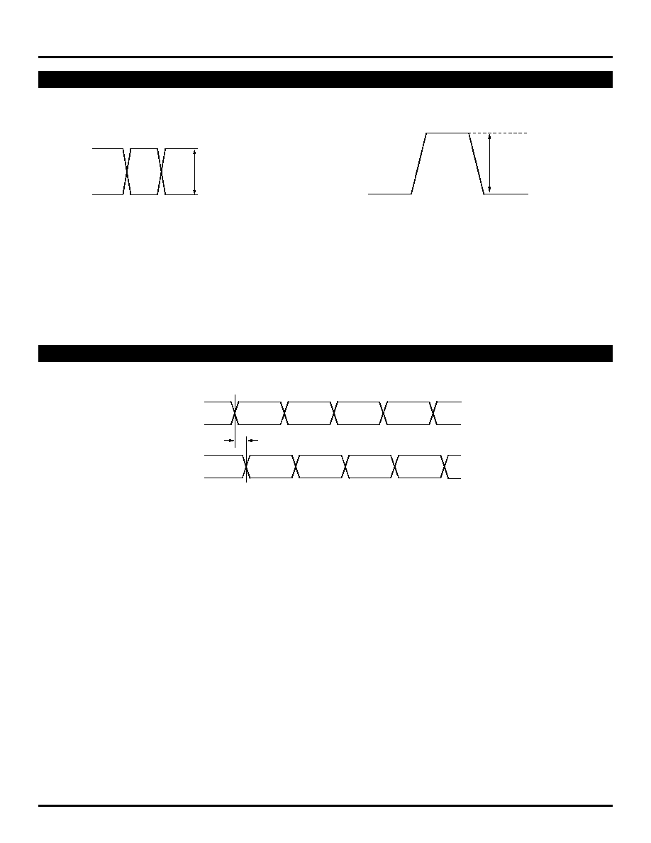
SINGLE-ENDED AND DIFFERENTIAL SWINGS
V
OUT
800mV (Typ.)
Figure 2a. Single-Ended Voltage Swing
V
DIFF_OUT
1600mV (Typ.)
Figure 2b. Differential Voltage Swing
TIMING DIAGRAM
IN
/IN
Q
/Q
t
pd
Figure 3. Timing Diagram
6
Precision Edgeģ
SY89327L
Micrel, Inc.
M9999-072005
hbwhelp@micrel.com or (408) 955-1690
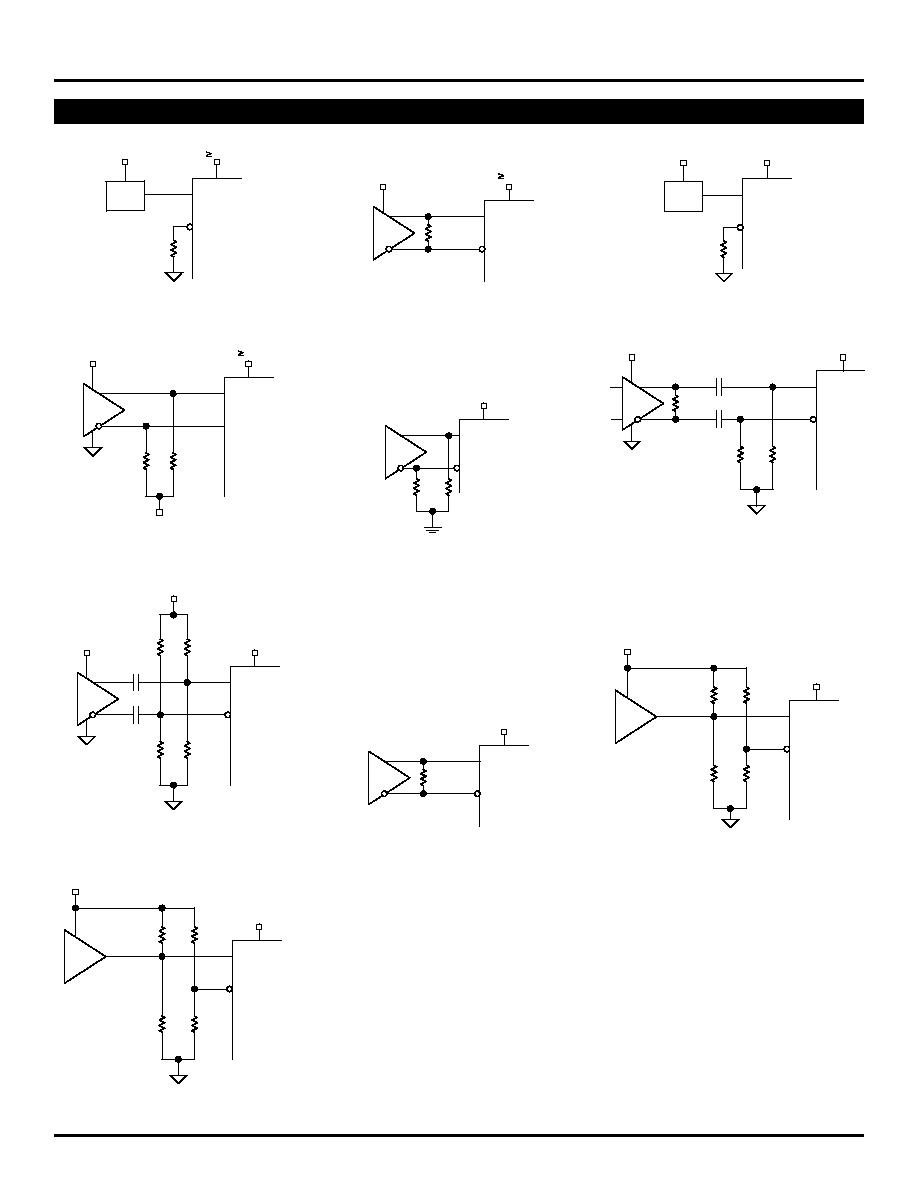
INPUT INTERFACE APPLICATIONS
IN
/IN SY89327L
LVTTL
2.5k
1%
V
CC(DRIVER)
V
CC(327)
V
CC(DRIVER)
Figure 4. 3.3V "TTL"
CML
IN
/IN
V
CC(DRIVER)
V
CC(327)
V
CC(DRIVER)
102
1%
SY89327L
Figure 5. CML-DC Coupled
IN
/IN
SY89327L
2.5V
LVTTL
2.5k
1%
2.3V to 2.7V
V
CC
Figure 6. 2.5V "TTL"
PECL
IN
/IN
51
1%
51
1%
V
CC(DRIVER)
V
CC(327)
V
CC(DRIVER)
SY89327L
V
CC
--2V
Figure 7. PECL-DC Coupled
HSTL
IN
/IN
SY89327L
V
CC
50
50
Figure 8. HSTL
CML
IN
/IN
3.92k
1%
3.92k
1%
102
1%
V
CC(DRIVER)
V
CC
SY89327L
Figure 9. CML-AC Coupled
Short Lines
CML
IN
/IN
130
1%
130
1%
V
CC(DRIVER)
V
CC
SY89327L
82
1%
82
1%
V
CC
Figure 10. CML-AC Coupled
Long Lines
LVDS
IN
/IN
V
CC
102
1%
SY89327L
Figure 11. LVDS
IN
/IN
100
1%
100
1%
V
CC
SY89327L
105
1%
105
1%
SSTL_2
V
DDQ
Figure 12. SSTL_2
IN
/IN
90.9
1%
90.9
1%
V
CC
SY89327L
110
1%
110
1%
SSTL_3
V
DDQ
Figure 13. SSTL_3

7
Precision Edge
ģ
SY89327L
Micrel, Inc.
M9999-072005
hbwhelp@micrel.com or (408) 955-1690
Part Number
Function
Data Sheet Link
SY55857L
3.3V, 2.5Gbps Any Input-to-LVPECL
www.micrel.com/product-info/products/sy55857l.shtml
Dual Translator
MLFTM Application Note
www.amkor.com/products/notes_papers/MLF_AppNote_0902.pdf
HBW Solutions
New Products and Applications
www.micrel.com/product-info/products/solutions.shtml
RELATED PRODUCT AND SUPPORT DOCUMENTATION

8
Precision Edgeģ
SY89327L
Micrel, Inc.
M9999-072005
hbwhelp@micrel.com or (408) 955-1690
8 LEAD
MicroLeadFrame (MLF-8)
Package Notes:
1. Package meets Level 2 qualification.
2. All parts are dry-packaged before shipment.
3. Exposed pads must be soldered to a ground for proper thermal management.
MICREL, INC.
2180 FORTUNE DRIVE
SAN JOSE, CA 95131
USA
TEL
+ 1 (408) 944-0800
FAX
+ 1 (408) 474-1000
WEB
http://www.micrel.com
The information furnished by Micrel in this data sheet is believed to be accurate and reliable. However, no responsibility is assumed by Micrel for its use.
Micrel reserves the right to change circuitry and specifications at any time without notification to the customer.
Micrel Products are not designed or authorized for use as components in life support appliances, devices or systems where malfunction of a product can
reasonably be expected to result in personal injury. Life support devices or systems are devices or systems that (a) are intended for surgical implant into
the body or (b) support or sustain life, and whose failure to perform can be reasonably expected to result in a significant injury to the user. A Purchaser's
use or sale of Micrel Products for use in life support appliances, devices or systems is at Purchaser's own risk and Purchaser agrees to fully indemnify
Micrel for any damages resulting from such use or sale.
© 2005 Micrel, Incorporated.