1
Precision Edge
Æ
SY89328L
Micrel, Inc.
M9999-072005
hbwhelp@micrel.com or (408) 955-1690
DESCRIPTION
s
3.3V
±
10% power supply
s
Guaranteed AC parameters over temperature:
f
MAX
> 275MHz (LVTTL)
s
< 2ns LVPECL-to-LVTTL propagation delay
s
< 600ps LVTTL-to-LVPECL propagation delay
s
Internal 75k
input pull-up and pull-down resistors
s
Industrial temperature range:
≠40
∞
C to +85
∞
C
s
Available in ultra-small 8-pin MLFTM
(2mm
◊◊
◊◊
◊
2mm)
package
FEATURES
Precision Edge
Æ
SY89328L
Rev.: B
Amendment: /0
Issue Date:
July 2005
The SY89328L is a differential LVPECL-to-LVTTL
translator and an LVTTL-to-differential LVPECL translator
in a single package. Because LVPECL (Positive ECL) levels
are used, only +3.3V and ground are required. The
SY89328L is functionally equivalent to the SY100EPT28L,
but in an ultra-small 8-lead MLFTM package that features a
70% smaller footprint. This ultra-small package and the dual
translation design of the SY89328L make it ideal for
applications that are sending and receiving signals across
a backplane.
Precision Edge
Æ
Precision Edge is a registered trademark of Micrel, Inc.
MicroLeadFrame and MLF are trademarks of Amkor Technology, Inc.
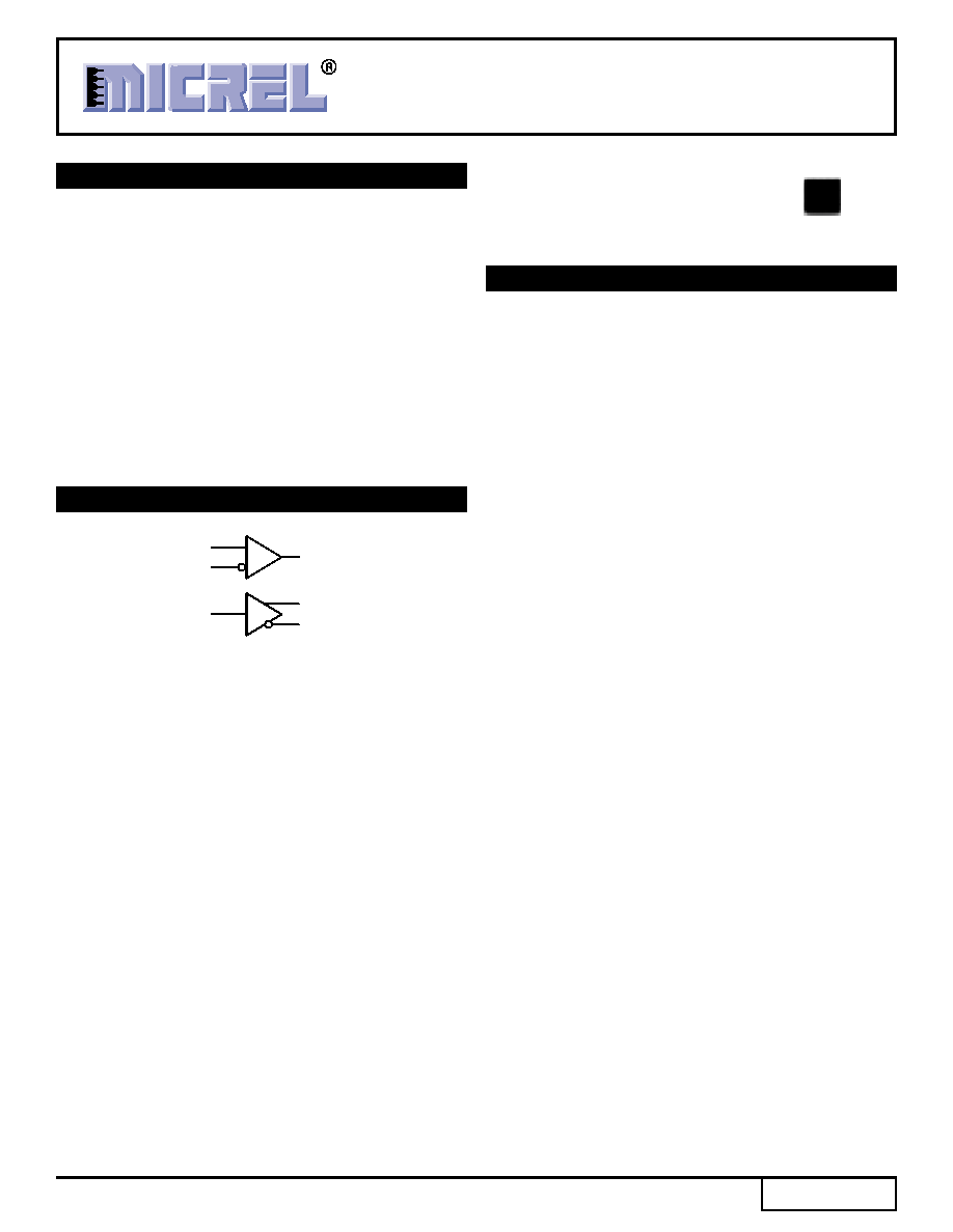
3V LVTTL-TO-DIFFERENTIAL
LVPECL AND DIFFERENTIAL
LVPECL-TO-LVTTL TRANSLATOR
BLOCK DIAGRAM
IN_LVPECL
/IN_LVPECL
Q_LVTTL
Q_LVPECL
/Q_LVPECL
IN_LVTTL
2
Precision Edge
Æ
SY89328L
Micrel, Inc.
M9999-072005
hbwhelp@micrel.com or (408) 955-1690
PIN DESCRIPTION
Pin Number
Pin Name
Type
Pin Function
1, 2
IN_LVPECL,
100k ECL Input
Differential LVPECL Input: Includes internal 75k
pull-down resistor on
`
/IN_LVPECL
internal 75k
pull-up and pull-down resistors on /IN.
See "Input Interface Applications" section for single-ended inputs.
7
Q_LVTTL
LVTTL Output
Single-ended LVTTL Output: Translated from LVPECL input. Q_LVTTL
output will default LOW with IN_LVPECL and /IN_LVPECL inputs left open.
6
IN_LVTTL
LVTTL Input
Single-ended LVTTL Input.
3, 4
Q_LVPECL,
100k ECL Output
Differential LVPECL Output: Translated from LVTTL input. See "Output
/Q_LVPECL
Interface Applications" section for recommendations on terminations.
8
VCC
VCC Power
Positive Power Supply: Bypass with 0.1
µ
F//0.01
µ
F low ESR capacitors.
5
GND,
Ground
GND and exposed pad must be tied to ground plane.
Exposed Pad
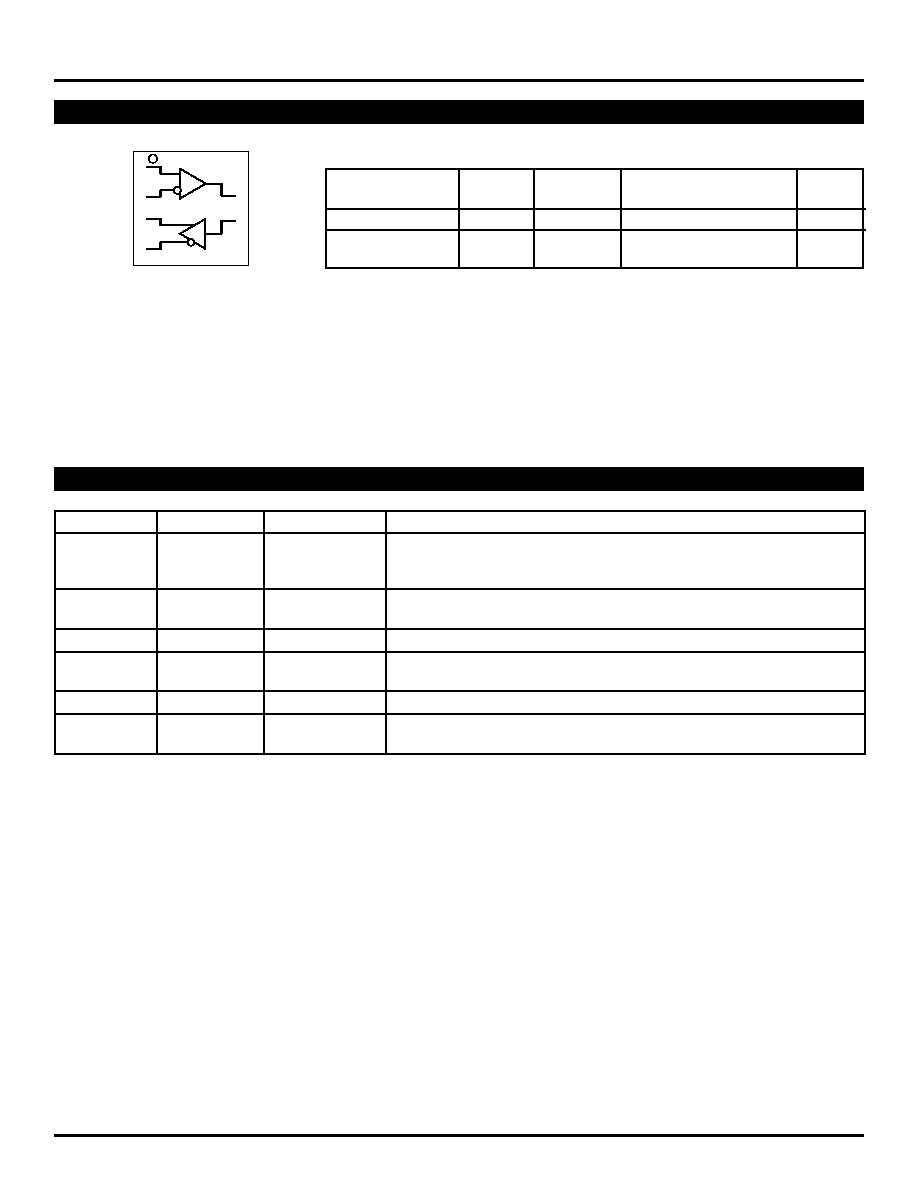
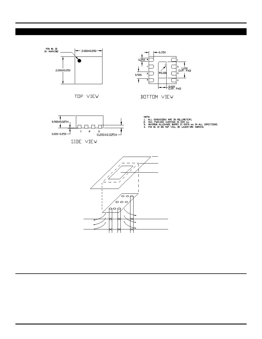
PACKAGE/ORDERING INFORMATION
IN_LVPECL
/IN_LVPECL
Q_LVPECL
/Q_LVPECL
VCC
Q_LVTTL
IN_LVTTL
GND
1
2
3
4
8
7
6
5
8-Pin MLFTM
Ultra-Small Outline (2mm
◊◊
◊◊
◊
2mm)
Ordering Information
Package
Operating
Package
Lead
Part Number
Type
Range
Marking
Finish
SY89328LMITR
MLF-8
Industrial
HEP28
Sn-Pb
SY89328LMGTR
MLF-8
Industrial
HEP28 with
Pb-Free
Pb-Free bar-line indicator
NiPdAu

3
Precision Edge
Æ
SY89328L
Micrel, Inc.
M9999-072005
hbwhelp@micrel.com or (408) 955-1690
Absolute Maximum Ratings
(Note 1)
Supply Voltage (V
CC
) .................................. ≠0.5V to +3.8V
Input Voltage (V
IN
) ......................................... ≠0.5V to V
CC
LVPECL Output Current (I
OUT
)
Continuous ............................................................. 50mA
Surge .................................................................... 100mA
Input Current
Source or sink current on IN, /IN ..........................
±
50mA
Lead Temperature (soldering, 20 sec.) ................... +260
∞
C
Storage Temperature (T
S
) ....................... ≠65
∞
C to +150
∞
C
Operating Ratings
(Note 2)
Supply Voltage (V
CC
) ...................................... 3.0V to 3.6V
Ambient Temperature (T
A
) ......................... ≠40
∞
C to +85
∞
C
Package Thermal Resistance, Note 3
MLFTM (
JA
)
Still-Air ................................................................. 93
∞
C/W
500lfpm ............................................................... 87
∞
C/W
MLFTM (
JB
)
Junction-to-Board ................................................ 60
∞
C/W
Symbol
Parameter
Condition
Min
Typ
Max
Units
V
CC
Power Supply Voltage
3.0
3.3
3.6
V
I
CC
Power Supply Current
Max V
CC
, No Load
22
40
mA
DC ELECTRICAL CHARACTERISTICS
(Note 4)
V
CC
= +3.3V
±
10% and V
EE
= 0V; R
L
= 50
to V
CC
≠2V; T
A
= ≠40
∞
C to +85
∞
C, unless otherwise noted.
Symbol
Parameter
Condition
Min
Typ
Max
Units
V
OH
Output HIGH Voltage
V
CC
≠1.145 V
CC
≠1.020 V
CC
≠0.895
V
V
OL
Output LOW Voltage
V
CC
≠1.945 V
CC
≠1.820 V
CC
≠1.695
V
V
IH
Input HIGH Voltage
V
CC
≠1.225
V
CC
≠0.880
V
V
IL
Input LOW Voltage
V
CC
≠1.945
V
CC
≠1.625
V
V
CMR
LVPECL Common Mode Range
1.2
V
CC
V
I
IH
Input HIGH Current
V
IN
= 3.46V
150
µ
A
I
IL
Input LOW Current
IN
0.5
µ
A
/IN
≠300
µ
A
Note 4.
The circuit is designed to meet the DC specifications shown in the above table after thermal equilibrium has been established.
LVPECL DC ELECTRICAL CHARACTERISTICS
(Note 4)
Note 1.
Permanent device damage may occur if ABSOLUTE MAXIMUM RATINGS are exceeded. This is a stress rating only and functional operation
is not implied at conditions other than those detailed in the operational sections of this data sheet. Exposure to ABSOLUTE MAXIMUM
RATlNG conditions for extended periods may affect device reliability.
Note 2.
The data sheet limits are not guaranteed if the device is operated beyond the operating ratings.
Note 3.
Package thermal resistance assumes exposed pad is soldered (or equivalent) to the devices most negative potential on the PCB.
4
Precision Edge
Æ
SY89328L
Micrel, Inc.
M9999-072005
hbwhelp@micrel.com or (408) 955-1690
V
CC
= +3.3V
±
10%. T
A
= ≠40
∞
C to +85
∞
C, unless otherwise noted.
Symbol
Parameter
Condition
Min
Typ
Max
Units
f
MAX
Maximum Frequency
LVPECL
Note 6
700
--
--
MHz
LVTTL
Note 7
275
350
--
MHz
t
pd
Propagation Delay
IN_LVPECL-to-Q_LVTTL
Note 7
1.5
--
2.5
ns
IN_LVTTL-to-Q_LVPECL
Note 6
100
400
600
ps
V
PP
LVPECL Input Voltage Swing
Note 8
100
--
--
mV
(Single-Ended)
t
DC
Duty Cycle
45
50
55
%
t
Jitter
Cycle-toCycle Jitter
Note 9
<1
ps
RMS
Total Jitter
Note 10
20
ps
PP
t
r
,
t
f
LVPECL Output Rise/Fall Times
At full output swing, Note 5
200
--
500
ns
(20% to 80%)
LVTTL Output Rise/Fall Times
At full output swing, Note 6
0.5
--
1.0
ns
(10% to 90%)
Note 5.
The circuit is designed to meet the DC specifications shown in the above table after thermal equilibrium has been established.
Note 6.
R
L
= 50
to V
CC
≠2V
Note 7.
C
L
= 20pF
Note 8.
V
PP
(min) is the minimum input swing for which AC parameters are guaranteed.
Note 9.
Cycle-to-cycle jitter definition: the variation of periods between adjacent cycles, T
n
≠ T
n≠1
,where T is the time between rising edges of the
output signal.
Note 10. Total jitter definition: with an ideal clock input of frequency
f
MAX
, no more than one output edge in 10
12
output edge will deviate by more than
the specified peak-to-peak jitter value.
AC ELECTRICAL CHARACTERISTICS
V
CC
= +3.3V
±
10%; C
L
= 20pF, T
A
= ≠40
∞
C to +85
∞
C, unless otherwise noted.
Symbol
Parameter
Condition
Min
Typ
Max
Units
V
OH
Output HIGH Voltage
I
OH
= ≠3mA
2.0
--
--
V
V
OL
Output LOW
Voltage
I
OH
= ≠24mA
--
--
0.5
V
V
IH
Input HIGH Voltage
2.0
--
--
V
V
IL
Input LOW Voltage
--
--
0.8
V
V
IK
Input Clamp Voltage
I
IK
= ≠18mA
--
--
≠1.2
V
I
IH
Input HIGH Current
V
IN
= 2.7V
--
--
20
µ
A
V
IN
= V
CC
--
--
100
µ
A
I
IL
Input LOW Current
V
IN
= 0.5V
--
--
≠0.2
µ
A
I
OUT(SC)
LVTTL Output
V
OUT
= 0V
≠275
--
≠80
mA
Short-Circuit Current
LVTTL DC ELECTRICAL CHARACTERISTICS
(Note 5)
5
Precision Edge
Æ
SY89328L
Micrel, Inc.
M9999-072005
hbwhelp@micrel.com or (408) 955-1690
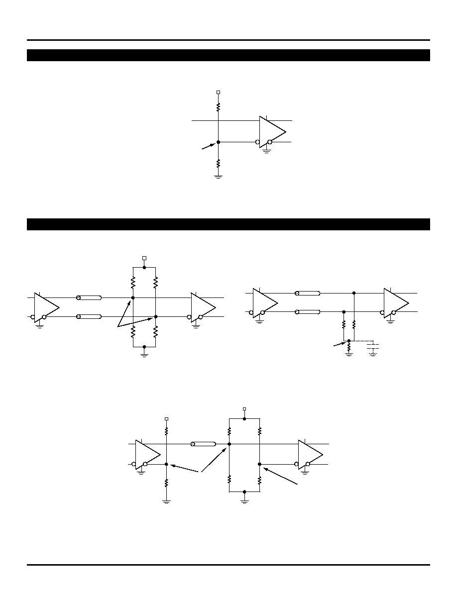
LVPECL INPUT INTERFACE APPLICATIONS
IN
+3.3V
V
CC
--1.3V
+3.3V
1k
1.6k
Figure 1. Single-Ended Input
(Terminating unused input)
LVPECL OUTPUT INTERFACE APPLICATIONS
Z
O
= 50
82
130
130
82
1k
1.6k
V
CC
--2V
V
CC
--1.3V
+3.3V
+3.3V
+3.3V
+3.3V
Figure 2c. Terminating Unused I/O
82
82
Z
O
= 50
Z
O
= 50
130
130
V
CC
--2V
+3.3V
+3.3V
+3.3V
Figure 2a. Parallel Thevenin-Equivalent
Termination
Z
O
= 50
Z
O
= 50
50
50
50
C (Optional)
0.01
µ
F
V
CC
--2V
+3.3V
+3.3V
Figure 2b. Three Resistor
"Y Termination"
6
Precision Edge
Æ
SY89328L
Micrel, Inc.
M9999-072005
hbwhelp@micrel.com or (408) 955-1690
MICREL, INC.
2180 FORTUNE DRIVE
SAN JOSE, CA 95131
USA
TEL
+ 1 (408) 944-0800
FAX
+ 1 (408) 474-1000
WEB
http://www.micrel.com
The information furnished by Micrel in this datasheet is believed to be accurate and reliable. However, no responsibility is assumed by Micrel for its use.
Micrel reserves the right to change circuitry and specifications at any time without notification to the customer.
Micrel Products are not designed or authorized for use as components in life support appliances, devices or systems where malfunction of a product can
reasonably be expected to result in personal injury. Life support devices or systems are devices or systems that (a) are intended for surgical implant into
the body or (b) support or sustain life, and whose failure to perform can be reasonably expected to result in a significant injury to the user. A Purchaser's
use or sale of Micrel Products for use in life support appliances, devices or systems is at Purchaser's own risk and Purchaser agrees to fully indemnify
Micrel for any damages resulting from such use or sale.
© 2005 Micrel, Incorporated.
8 LEAD ULTRA-SMALL EPAD-
MicroLeadFrameTM (MLF-8)
Package
EP- Exposed Pad
Die
CompSide Island
Heat Dissipation
Heavy Copper Plane
Heavy Copper Plane
V
EE
V
EE
Heat Dissipation
PCB Thermal Consideration for 8-Pin MLFTM Package
Package Notes:
Note 1.
Package meets Level 2 qualification.
Note 2.
All parts are dry-packaged before shipment.
Note 3.
Exposed pads must be soldered to a ground for proper thermal management.