
DESCRIPTION
s
Integrated synthesizer plus fanout buffers, clock
drivers, and translator in a single 64-pin package
s
3.3V
±
10% power supply
s
Low jitter: <50ps cycle-to-cycle
s
Low pin-to-pin skew: <50ps
s
33MHz to 500MHz output frequency range
s
Direct interface to crystal: 14MHz to 18MHz
s
LVPECL/HSTL outputs
s
TTL/CMOS compatible control logic
s
3 independently programmable output frequency
banks:
∑ 9 differential output pairs @BankB (HSTL)
∑ 2 differential output pairs @BankA (LVPECL)
∑ 2 differential output pairs @BankC (LVPECL)
s
ExtVCO input allows synthesizer and crystal
interface to be bypassed
s
Available in 64-pin EPAD-TQFP
FEATURES
3.3V, PRECISION, 33MHz to 500MHz
PROGRAMMABLE LVPECL AND HSTL
BUS CLOCK SYNTHESIZER
Precision EdgeTM
SY89531L
APPLICATIONS
s
Servers
s
Workstations
s
Parallel processor-based systems
s
Other high-performance computing
s
Communications
1
Rev.: A
Amendment: /0
Issue Date:
June 2003
The SY89531L programmable clock synthesizer/driver is
part of a 3.3V, high-frequency, precision PLL-based clock
synthesizer family optimized for multi-frequency, multi-
processor server, enterprise networking and other computing
applications that require the highest precision and integration.
The device integrates the following blocks into a single
monolithic IC:
∑ PLL (Phase-Lock-Loop)-based synthesizer
∑ Fanout buffers
∑ Clock generator (dividers)
∑ Logic translation (LVPECL, HSTL)
This level of integration minimizes the additive jitter and
part-to-part skew associated with the discrete alternative,
resulting in superior system-level timing as well as reduced
board space and power. For applications that must interface
to a reference clock, see the SY89536L.
Data sheets and support documentation can be found on
Micrel's web site at www.micrel.com.
PRODUCT SELECTION GUIDE
Input
Output
Device
Crystal
Reference
BankA
BankB
BankC
SY89531L
X
LVPECL
HSTL
LVPECL
SY89532L*
X
LVPECL LVPECL LVPECL
SY89533L*
X
LVPECL
LVDS
LVPECL
SY89534L*
X
LVPECL LVPECL LVPECL
SY89535L*
X
LVPECL
LVDS
LVPECL
SY89536L*
X
LVPECL
HSTL
LVPECL
*Refer to individual data sheet for details.
Precision EdgeTM
Precision Edge is a trademark of Micrel, Inc.
2
SY89531L
Micrel
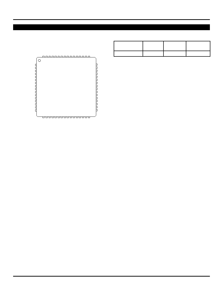
PACKAGE/ORDERING INFORMATION
Ordering Information
Package
Operating
Package
Part Number
Type
Range
Marking
SY89531LHC
H64-1
Commercial
SY89531LHC
VCC_LOGIC
QB0
VCCOB
/QA1
QA1
/QA0
QA0
VCCO
A
FSEL_A2
FSEL_A1
FSEL_A0
OUT_SYNC
VCC_LOGIC
VCCA
GND
NC
NC
NC
NC
VCO_SEL
/EXTVCO
EXTVCO
LOOP_REF
LOOP_FILTER
GND
XTAL2
XTAL1
VBB_REF
M(3)
M(2)
M(1)
M(0)
/QB0
QB1
/QB1
QB2
/QB2
QB3
/QB3
QB4
/QB4
QB5
/QB5
QB6
/QB6
QB7
/QB7
QB8
64
1
2
3
4
5
6
7
8
9
10
11
12
13
14
15
16
48
47
46
45
44
43
42
41
40
39
38
37
36
35
34
33
63 62 61 60 59 58 57 56 55 54 53 52 51 50 49
17 18 19 20 21 22 23 24 25 26 27 28 29 30 31 32
QC0
/QB8
VCCOB
VCCOB
GND
FSEL_B0
FSEL_B1
FSEL_B2
GND
FSEL_C0
FSEL_C1
FSEL_C2
VCCOC
/QC0
QC1
/QC1
64-Pin EPAD-TQFP (H64-1)
3
SY89531L
Micrel
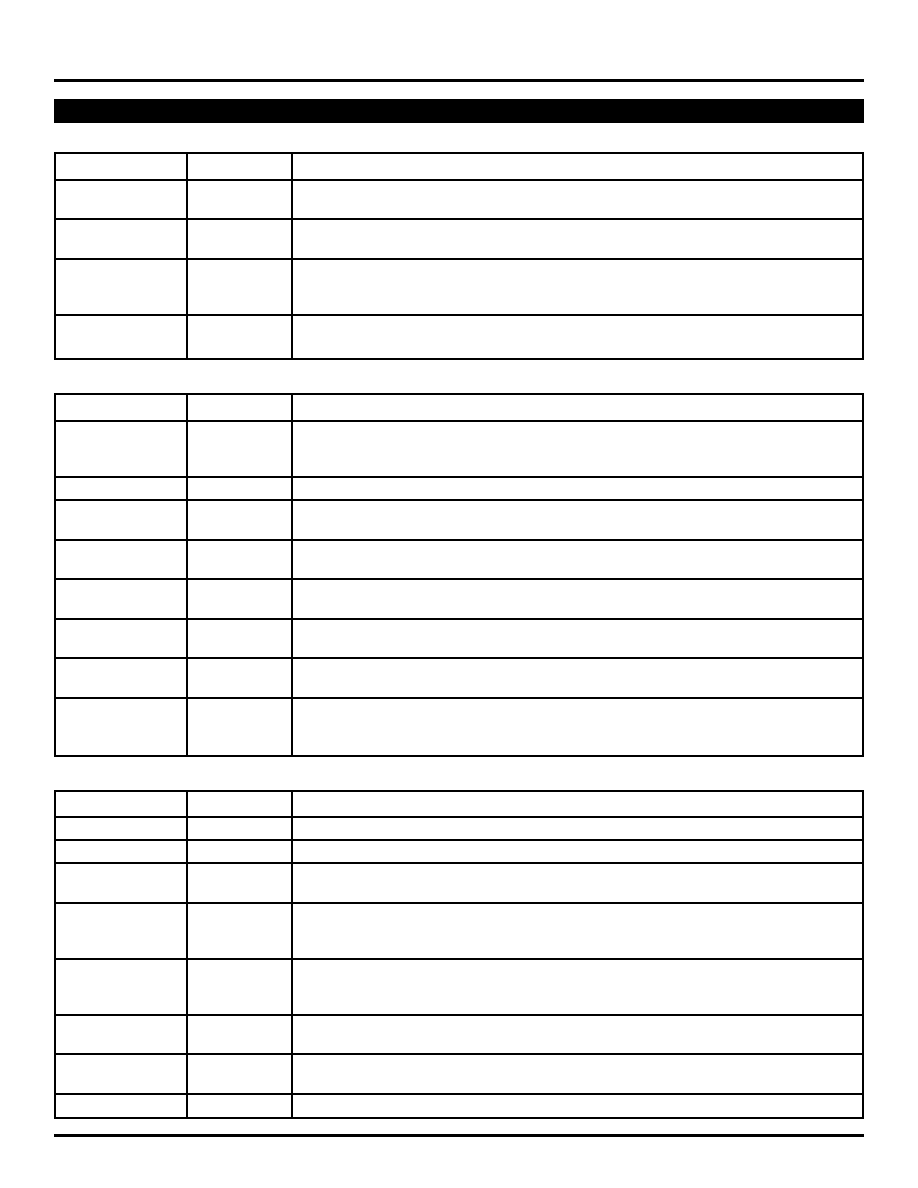
PIN DESCRIPTION
Power
Pin Number
Pin Name
Pin Function
60, 61
V
CC_Logic
Power for Core Logic: Connect to 3.3V supply. 3.3V power pins are not internally
connected on the die, and must be connected together on the PCB.
62
V
CCA
Power for PLL: Connect to "quiet" 3.3V supply. 3.3V power pins are not internally
connected on the die, and must be connected together on the PCB.
55
V
CCO
A
Power for Output Drivers: Connect all V
CCO
A and V
CCO
C pins to 3.3V supply and V
CCO
B
30, 31, 50
V
CCO
B
pins to 1.8V supply.
21
V
CCO
C
9, 25, 63, 29
GND
Ground: Exposed pad must be soldered to a ground plane.
(exposed pad)
Configuration
Pin Number
Pin Name
Pin Function
4
VCO_SEL
LVTTL/CMOS Compatible Input: Selects between internal or external VCO. For
external VCO, leave floating. Default condition is logic HIGH. Internal 25k
pull-up.
When tied LOW, internal VCO is selected.
7
LOOP REF
Analog Input/Output: Provides the reference voltage for PLL loop filter.
8
LOOP FILTER
Analog Input/Output: Provides the loop filter for PLL. See
"External Loop Filter
Considerations"
for loop filter values.
13,14,15,16
M (3:0)
LVTTL/CMOS Compatible Input: Used to change the PLL feedback divider. Internal 25k
pull-up. M0 = LSB. Default is logic HIGH. See
"Feedback Divide Select"
table.
22, 23, 24
FSEL_C (2:0)
LVTTL/CMOS Compatible Input: Bank C post divide select. Internal 25k
pull-up.
Default is logic HIGH. See
"Post-Divide Frequency Select"
table. FSEL_C0 = LSB.
26, 27, 28
FSEL_B (2:0)
LVTTL/CMOS Compatible Input: Bank B post divide select. Internal 25k
pull-up.
Default is logic HIGH. See
"Post-Divide Frequency Select"
table. FSEL_B0 = LSB.
56, 57, 58
FSEL_A (2:0)
LVTTL/CMOS Compatible Input: Bank A post divide select. Internal 25k
pull-up.
Default is logic HIGH. See
"Post-Divide Frequency Select"
table. FSEL_A0 = LSB.
59
OUT_SYNC
Banks A, B, C Output Synchronous Control: (LVTTL/CMOS compatible). Internal 25k
pull-up. After any bank has been programmed, toggle with a HIGH-LOW-HIGH
pulse to resynchronize all output banks.
Input/Output
Pin Number
Pin Name
Pin Function
1, 2, 3
NC
No Connect: Leave floating.
10, 11
XTAL2, XTAL1
Crystal Input. Directly connect a series resonant crystal across inputs.
12
VBB_REF
Reference Output Voltage. Used for single-ended input. Maximum sink/source
current = 0.5mA.
5, 6
/EXT_VCO,
Differential "Any In" Compatible Input Pair. Allows for external VCO connection. The "Any
EXT_VCO
In" input structure accepts many popular logic types. See
"Input Interface for ExtVCO Pins"
section for interface diagrams. Can leave unconnected if using internal VCO.
51, 52, 53, 54
QA1 to QA0
Bank A 100k LVPECL Output Drivers: Output frequency is controlled by FSEL_A
(0:2). Terminate outputs with 50
to V
CC
≠2V. See
"Output Termination
Recommendations"
section.
32≠49
QB8 to QB0
Bank B Output Drivers: Differential HSTL outputs. See
"Output Termination Recommendations"
section. Output frequency is controlled by FSEL_B (0:2).
17, 18, 19, 20
QC1 to QC0
Bank C 100k LVPECL Output Drivers: Output frequency is controlled by FSEL_C (0:2).
Terminate outputs with 50
to V
CC
≠2V. See
"Output Termination Recommendations"
section.
64
NC
No Connect: Leave floating.
4
SY89531L
Micrel
Absolute Maximum Ratings
(Note 1)
Supply Voltage (V
IN
) ................................... ≠0.5V to +4.0V
V
CC
Pin Potential to Ground Pin (All V
CC
) .. ≠0.5V to +4.0V
Input Voltage (except XTAL 1,2 pins) (V
IN
) ... ≠0.5V to V
CCI
XTAL 1, 2 Input Voltage (V
XTAL 1,2
) ...... (V
CC
≠1.9V) to V
CC
DC Output Current (I
OUT
)
≠LVPECL, HSTL outputs ..................................... ≠50mA
Lead Temperature (soldering, 10 sec.) ..................... 220
∞
C
Storage Temperature (T
S
) ....................... ≠65
∞
C to +150
∞
C
Operating Ratings
(Note 2)
Supply Voltage
V
CCO
A and V
CCO
C ...................................... 3.0V to 3.6V
V
CCO
B ......................................................... 1.6V to 2.0V
Ambient Temperature (T
A
) ............................. 0
∞
C to +85
∞
C
Package Thermal Resistance (Junction-to-Ambient)
With Die attach soldered to GND:
TQFP (
JA
) Still-Air .............................................. 23
∞
C/W
TQFP (
JA
) 200lfpm ............................................ 18
∞
C/W
TQFP (
JA
) 500lfpm ............................................ 15
∞
C/W
With Die attach NOT soldered to GND, Note 3
TQFP (
JA
) Still-Air .............................................. 44
∞
C/W
TQFP (
JA
) 200lfpm ............................................ 36
∞
C/W
TQFP (
JA
) 500lfpm ............................................ 30
∞
C/W
Package Thermal Resistance (Junction-to-Case)
TQFP
(
JC
) ......................................................... 4.3
∞
C/W
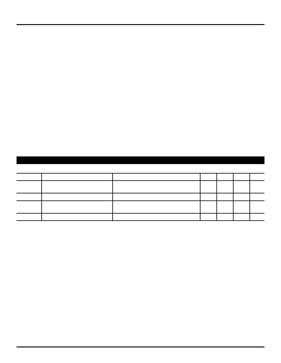
Power Supply
Symbol
Parameter
Condition
Min
Typ
Max
Units
V
CCA
PLL and Logic Supply Voltage
Note 4
3.0
3.3
3.6
V
V
CC_Logic
V
CCO
A/C
Bank A and C V
CC
Output
3.0
3.3
3.6
V
V
CCO
B
Bank B V
CC
Output
LVPECL/HSTL
1.6
1.8
2.0
V
I
CC
Total Supply Current
Note 5
--
230
295
mA
DC ELECTRICAL CHARACTERISTICS
Note 1.
Permanent device damage may occur if ABSOLUTE MAXIMUM RATINGS are exceeded. This is a stress rating only and functional operation is
not implied at conditions other than those detailed in the operational sections of this data sheet. Exposure to ABSOLUTE MAXIMUM RATlNG
conditions for extended periods may affect device reliability.
Note 2.
The data sheet limits are not guaranteed if the device is operated beyond the operating ratings.
Note 3.
It is recommended that the user always solder the exposed die pad to a ground plane for enhanced heat dissipation.
Note 4.
V
CCA
, V
CC_LOGIC
, V
CCO
A/C are
not
internally connected together inside the device. They must be connected together on the PCB. V
CCO
B is a
separate supply.
Note 5.
No load. Outputs floating, Banks A, B, and C enabled.
5
SY89531L
Micrel
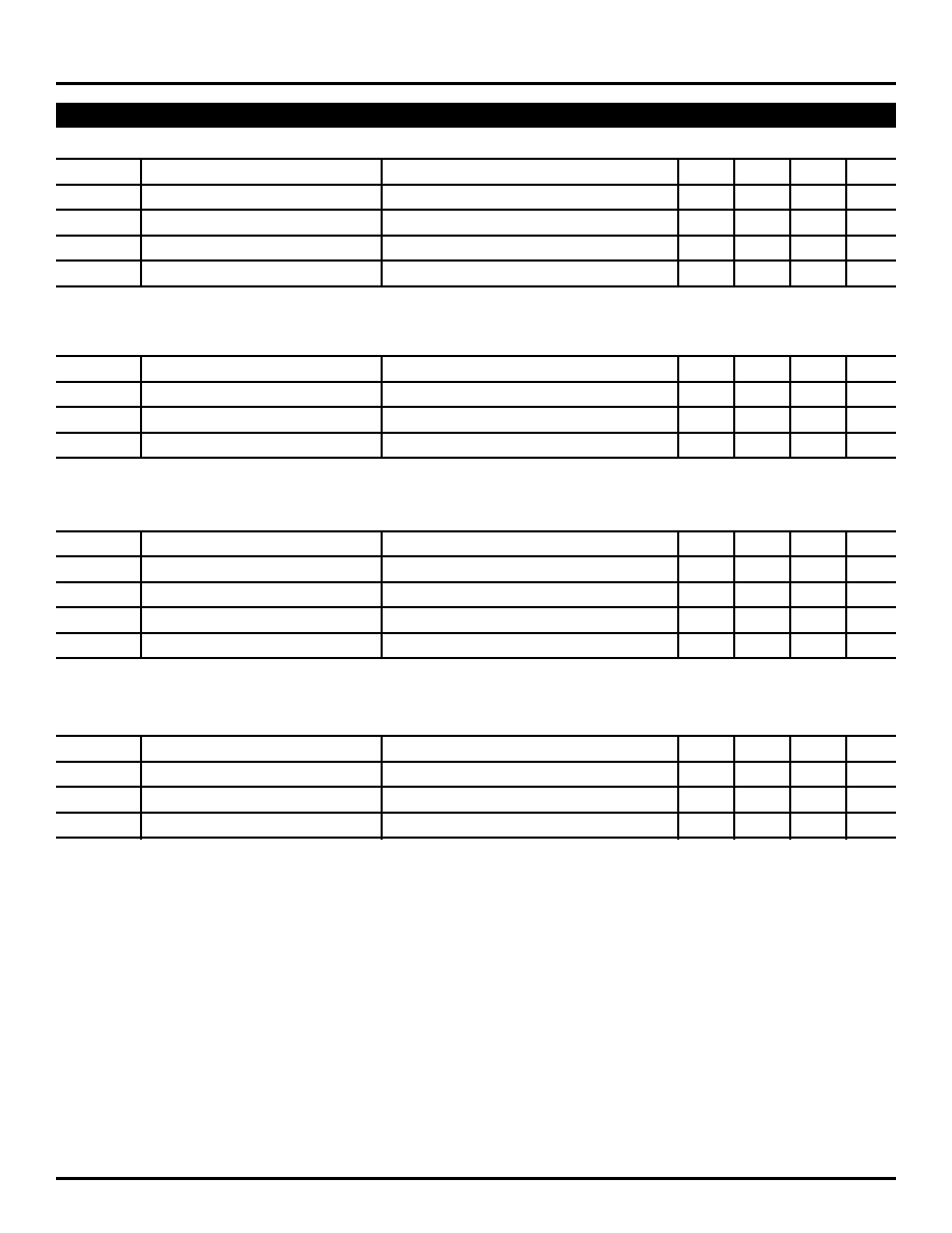
DC ELECTRICAL CHARACTERISTICS
LVCMOS/LVTTL Input Control Logic (V
CCA
,
V
CC_LOGIC
, V
CCO
A/C = +3.3V
±
10%)
Symbol
Parameter
Condition
Min
Typ
Max
Units
V
IH
Input HIGH Voltage
2.0
--
--
V
V
IL
Input LOW Voltage
--
--
0.8
V
I
IH
Input HIGH Current
--
--
150
µ
A
I
IL
Input LOW Current
--
--
≠300
µ
A
ExtVCO (Pins 5, 6) INPUT (All V
CC
pins except V
CCO
B = +3.3V
±
10%, V
CCO
B = +1.8V
±
10%)
Symbol
Parameter
Condition
Min
Typ
Max
Units
V
ID
Differential Input Voltage
100
--
--
mV
V
IH
Input HIGH Voltage
--
--
V
CC
+0.3
V
V
IL
Input LOW Voltage
≠0.3
--
--
V
100K LVPECL Output (All V
CC
pins except V
CCO
B = +3.3V
±
10%, V
CCO
B = +1.8V
±
10%)
(Note 6)
Symbol
Parameter
Condition
Min
Typ
Max
Units
V
OH
Output HIGH Voltage
V
CC
≠1.145 V
CC
≠1.020 V
CC
≠0.895
V
V
OL
Output LOW Voltage
V
CC
≠1.945 V
CC
≠1.820 V
CC
≠1.695
V
V
BB
Output Reference Voltage
V
CC
≠1.325 V
CC
≠1.425 V
CC
≠1.525
V
V
OUT
Output Voltage Swing
--
800
--
mV
HSTL Output (Bank B QB0:8) (All V
CC
pins except V
CCO
B = +3.3V
±
10%, V
CCO
B = +1.8V
±
10%)
(Note 7)
Symbol
Parameter
Condition
Min
Typ
Max
Units
V
OUT
Output Voltage Swing
--
800
--
mV
V
OH
Output HIGH Voltage
1.0
--
1.2
V
V
OL
Output LOW Voltage
0.2
--
0.4
V
Note 6.
All LVPECL outputs loaded with 50
to V
CC
≠2V.
Note 7.
All HSTL outputs loaded with 50
to GND.