1
Precision EdgeTM
SY89823L
Micrel
M9999-031804
hbwhelp@micrel.com or (408) 955-1690
FEATURES
s
22 differential HSTL (low-voltage swing) output pairs
s
HSTL outputs drive 50
to ground with no offset
voltage
s
3.3V core supply, 1.8V output supply for reduced
power
s
LVPECL and HSTL inputs
s
Low part-to-part skew (200ps max.)
s
Low pin-to-pin skew (50ps max.)
s
Triple-buffered output enable (OE)
s
≠40
∞
C to +85
∞
C temperature range
s
Available in a 64-pin EPAD-TQFP
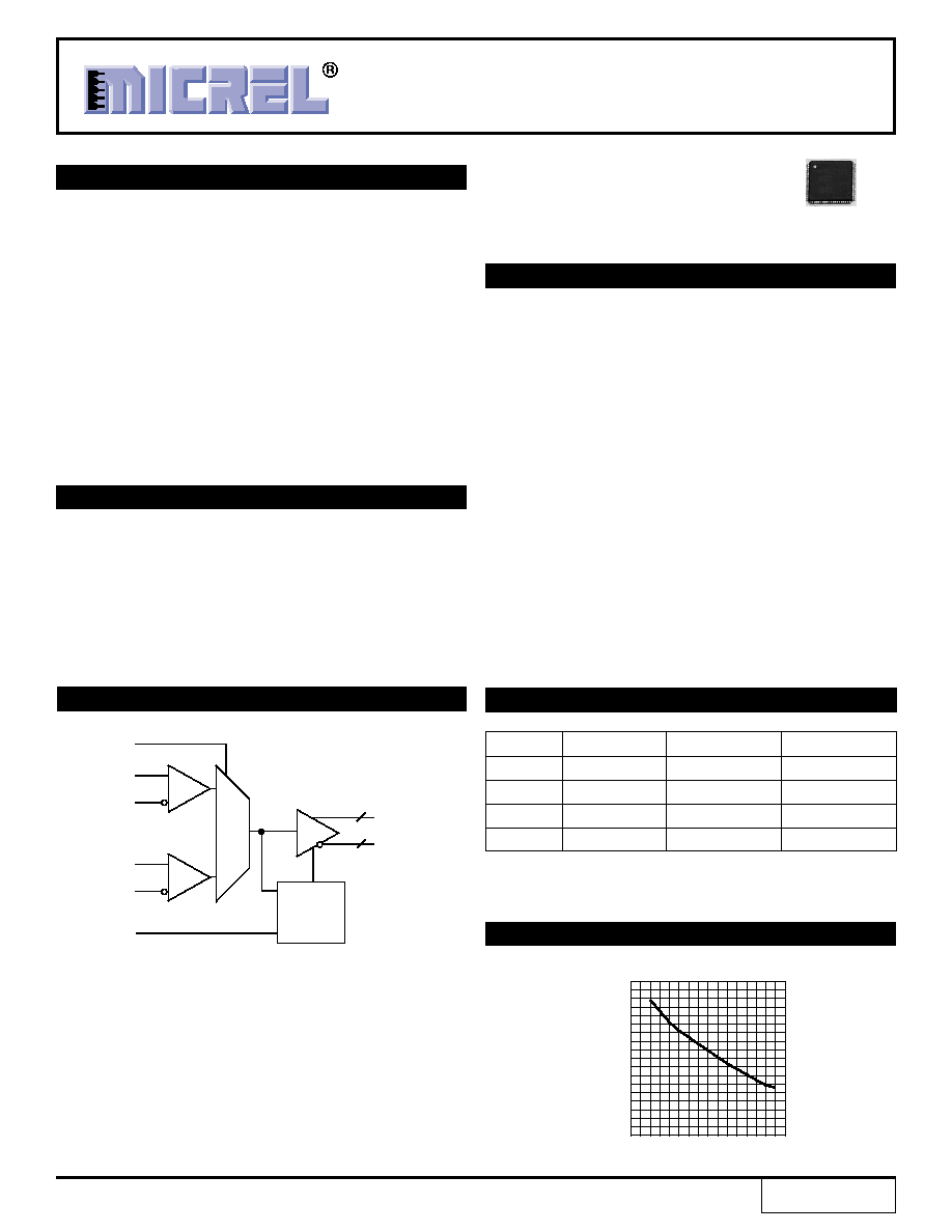
The SY89823L is a high-performance bus clock driver with 22
differential High-Speed Transceiver Logic (HSTL), 1.5V compatible
output pairs. The device is designed for use in low-voltage (3.3V/
1.8V) applications that require a large number of outputs to drive
precisely aligned, ultra-low skew signals to their destination. The
input is multiplexed from either HSTL or Low-Voltage Positive-
Emitter-Coupled Logic (LVPECL) by the CLK_SEL pin.
The Output Enable (OE) is synchronous and triple-buffered so
that the outputs will only be enabled/disabled when they are already
in the LOW state. This avoids any potential of generating a runt clock
pulse when the device is enabled/disabled, as can occur with an
asynchronous control. The triple-buffering feature provides a three-
clock delay from the time the OE input is asserted/de-asserted to
when the clock appears at the outputs.
The SY89823L features low pin-to-pin skew (50ps max.) and low
part-to-part skew (200ps max.), performance previously unachievable
in a standard product having such a high number of outputs. The
SY89823L is available in a single, space-saving package, enabling
a lower overall cost solution.
All support documentation can be found on Micrel's web site at
www.micrel.com.
3.3V, 500MHz 1:22
DIFFERENTIAL HSTL (1.5V)
FANOUT BUFFER/TRANSLATOR
DESCRIPTION
Precision EdgeTM
SY89823L
LOGIC SYMBOL
CLK_SEL
HSTL_CLK
/HSTL_CLK
LVPECL_CLK
/LVPECL_CLK
OE
0
1
22
22
Q0 - Q21
/Q0 - /Q21
EN
ENABLE
LOGIC
Rev.: A
Amendment: /0
Issue Date:
March 2004
Precision EdgeTM
Precision Edge is a trademark of Micrel, Inc.
OE
(1)
CLK_SEL
Q
0
-Q
21
/Q
0
-/Q
21
0
0
LOW
HIGH
0
1
LOW
HIGH
1
0
HSTL_CLK
/HSTL_CLK
1
1
LVPECL_CLK
/LVPECL_CLK
Note:
1. The output enable (OE) signal is synchronized with the low level of the
HSTL_CLK and LVPECL_CLK signal.
TRUTH TABLE
APPLICATIONS
s
High-performance PCs
s
Workstations
s
Parallel processor-based systems
s
Other high-performance computing
s
Communications
TYPICAL PERFORMANCE
0
100
200
300
400
500
600
700
800
900
0 0.2 0.4 0.6 0.8 1 1.2 1.4 1.6
OUTPUT AMPLITUDE (mV)
OUTPUT FREQUENCY (GHz)
Output Amplitude
vs. Frequency
2
Precision EdgeTM
SY89823L
Micrel
M9999-xxxx
hbwhelp@micrel.com or (408) 955-1690
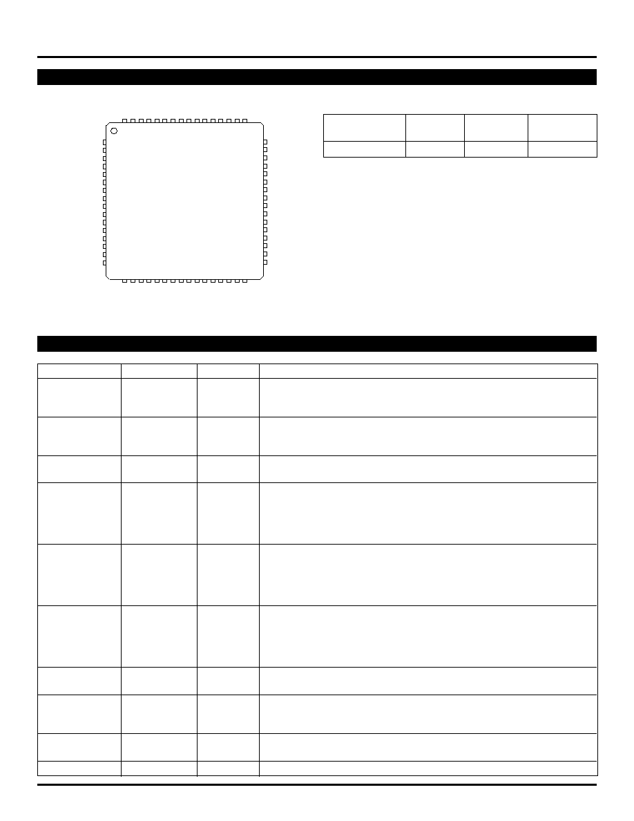
PACKAGE/ORDERING INFORMATION
Ordering Information
Package
Operating
Package
Part Number
Type
Range
Marking
SY89823LHI
H64-1
Industrial
SY89823LHI
Q1
VCCO
Q6
Q6
Q5
Q5
Q4
Q4
Q3
Q3
Q2
Q2
Q1
Q0
Q0
VCCO
VCCO
NC
NC
VCCI
HSTL_CLK
/HSTL_CLK
CLK_SEL
LVPECL_CLK
/LVPECL_CLK
GND
OE
NC
NC
/Q21
Q21
VCCO
VCCO
Q7
/Q7
Q8
/Q8
Q9
/Q9
Q10
/Q10
Q11
/Q11
Q12
/Q12
Q13
/Q13
VCCO
64
1
2
3
4
5
6
7
8
9
10
11
12
13
14
15
16
48
47
46
45
44
43
42
41
40
39
38
37
36
35
34
33
63 62 61 60 59 58 57 56 55 54 53 52 51 50 49
17 18 19 20 21 22 23 24 25 26 27 28 29 30 31 32
/Q19
VCCO
Q14
/Q14
Q15
/Q15
Q16
/Q16
Q17
/Q17
Q18
/Q18
Q19
Q20
/Q20
VCCO
64-Pin EPAD-TQFP (H64-1)
PIN DESCRIPTION
Pin Number
Pin Name
Type
Pin Function
5, 6
HSTL_CLK,
HSTL
Differential clock input selected by CLK_SEL. Can be left floating if not
/HSTL_CLK
Input
selected. Floating input, if selected, produces an indeterminate output. HSTL
input signal requires external termination 50
to GND.
8, 9
LVPECL_CLK,
LVPECL
Differential clock input selected by CLK_SEL. Can be left floating. Floating
/LVPECL_CLK
Input
input, if selected, produces a LOW at the output. Requires external
termination. 75k
pull-up.
7
CLK_SEL
LVTTL
Selects HSTL_CLK input when LOW and LVPECL_CLK output when HIGH.
Input
11k
pull-up. Default condition selects LVPECL_CLK if left open.
11
OE
LVTTL
Enable input synchronized internally to prevent glitching of the Q0-Q21 and
Input
/Q0≠/Q21 outputs. Must be a minimum of three clock periods wide if
synchronous with the CLK inputs and must meet the t
S
and t
H
requirements
(refer to "AC Electrical Characteristics" section ). If asynchronous, must be a
minimum of four clock periods wide. 11k
pull-up.
63, 61, 59, 57, 55,
Q0≠Q21
HSTL
Differential clock outputs from HSTL_CLK when CLK_SEL = LOW and
53, 51, 47, 45, 43,
Output
LVPECL outputs when CLK_SEL = HIGH. HSTL outputs must be terminated
41, 39, 37, 35, 31,
with 50
to GND. Q0≠Q21 outputs are static LOW when OE = LOW.
29, 27, 25, 23, 21,
Unused output pairs may be left floating.
19, 15
62, 60, 58, 56, 54,
/Q0≠/Q21
HSTL
Differential clock outputs from HSTL_CLK when CLK_SEL = LOW and
52, 50, 46, 44, 42,
Output
LVPECL outputs when CLK_SEL = HIGH. HSTL outputs must be terminated
40, 38, 36, 34, 30,
with 50
to GND. /Q0≠/Q21 outputs are static HIGH when OE = LOW.
28, 26, 24, 22, 20,
Unused output pairs may be left floating.
18, 14
4
VCCI
VCC Core
Core V
CC
connected to 3.3V supply. Bypass with 0.1
µ
F in parallel with
Power
0.01
µ
F low ESR capacitors as close to V
CCI
pins as possible.
1, 16, 17, 32,
VCCO
VCC Output
Output Buffer V
CC
connected to 1.8V supply. Bypass with 0.1
µ
F in parallel
33, 48, 49, 64
Power
with 0.01
µ
F low ESR capacitors as close to V
CCO
pin as possible. All V
CCO
pins should be connected together on the PCB.
10
GND,
Ground pin and exposed pad must be connected to the same ground plane.
Exposed Pad
2, 3, 12, 13
NC
No Connect.
3
Precision EdgeTM
SY89823L
Micrel
M9999-031804
hbwhelp@micrel.com or (408) 955-1690
DC ELECTRICAL CHARACTERISTICS
(4)
Absolute Maximum Ratings
(1)
Supply Voltage (V
IN
) ..................................... ≠0.5V to V
CCI
V
CC
Pin Potential to Ground Pin
V
CCI,
V
CCO ...........................................................
≠0.5V to +4.0V
DC Output Current, Output HIGH (I
OUT
) .................. ≠50mA
Lead Temperature (soldering, 10 sec.) ..................... 220
∞
C
Storage Temperature (T
S
) ....................... ≠65
∞
C to +150
∞
C
Operating Ratings
(2)
Supply Voltage
V
CCI ..................................................................
+3.15V to +3.45V
V
CCO .....................................................................
+1.6V to +2.0V
Ambient Temperature (T
A
) ......................... ≠40
∞
C to +85
∞
C
Package Thermal Resistance
(3)
EPAD-TQFP
(
JA
) with Die attach soldered to GND
Still-Air ............................................................. 23
∞
C/W
200lfpm ............................................................ 18
∞
C/W
500lfpm ............................................................ 15
∞
C/W
with Die attach NOT soldered to GND
Still-Air ............................................................. 44
∞
C/W
200lfpm ............................................................ 36
∞
C/W
500lfpm ............................................................ 30
∞
C/W
EPAD-TQFP
(
JC
) .............................................. 4.3
∞
C/W
Power Supply T
A
= ≠40
∞
C to +85
∞
C, unless otherwise stated.
Symbol
Parameter
Condition
Min
Typ
Max
Units
V
CCI
V
CC
Core
3.15
3.3
3.45
V
V
CCO
V
CC
Output
1.6
1.8
2.0
V
I
CCI
I
CC
Core
Max V
CC
, no load
--
115
170
mA
HSTL V
CCI
= 3.3V
±
5%; V
CCO
= 1.8V
±
10%; R
L
= 50
to GND; T
A
= ≠40
∞
C to +85
∞
C, unless otherwise stated.
Symbol
Parameter
Condition
Min
Typ
Max
Units
V
OH
Output HIGH Voltage
1.0
--
1.2
V
V
OL
Output LOW Voltage
0.2
--
0.4
V
V
IH
Input HIGH Voltage
V
X
+0.1
--
1.6
V
V
IL
Input LOW Voltage
≠0.3
--
V
X
≠0.1
V
V
X
Input Crossover Voltage
0.68
--
0.9
V
I
IH
Input HIGH Current
+20
--
≠350
µ
A
I
IL
Input LOW Current
--
--
≠500
µ
A
LVPECL V
CCI
= 3.3V
±
5%; V
CCO
= 1.8V
±
10%; T
A
= ≠40
∞
C to +85
∞
C, unless otherwise stated.
Symbol
Parameter
Condition
Min
Max
Units
V
IH
Input HIGH Voltage
V
CCI
≠ 1.165 V
CCI
≠ 0.880
V
V
IL
Input LOW Voltage
V
CCI
≠ 1.810 V
CCI
≠ 1.475
V
I
IH
Input HIGH Current
--
+150
µ
A
I
IL
Input LOW Current
0.5
--
µ
A
Notes:
1. Permanent device damage may occur if the ratings in the "Absolute Maximum Ratings" section are exceeded. This is a stress rating only and
functional operation is not implied at conditions other than those detailed in the operational sections of this data sheet. Exposure to absolute
maximum ratings conditions for extended periods may affect device reliability.
2. The data sheet limits are not guaranteed if the device is operated beyond the operating ratings.
3. Valid for 4-layer board.
4. The circuit is designed to meet the DC specifications shown in the above table after thermal equilibrium has been established.
4
Precision EdgeTM
SY89823L
Micrel
M9999-xxxx
hbwhelp@micrel.com or (408) 955-1690
DC ELECTRICAL CHARACTERISTICS
(5)
LVCMOS/LVTTL V
CCI
= 3.3V
±
5%; V
CCO
= 1.8V
±
10%; T
A
= ≠40
∞
C to +85
∞
C, unless otherwise stated.
Symbol
Parameter
Condition
Min
Typ
Max
Units
V
IH
Input HIGH Voltage
2.0
--
--
V
V
IL
Input LOW Voltage
--
--
0.8
V
I
IH
Input HIGH Current
+20
--
≠250
µ
A
I
IL
Input LOW Current
--
--
≠600
µ
A
V
CCI
= 3.3V
±
5%; V
CCO
= 1.8V
±
10%; All outputs loaded with 50
to GND; T
A
= ≠40
∞
C to +85
∞
C, unless otherwise stated.
Symbol
Parameter
Condition
Min
Typ
Max
Units
f
MAX
Maximum Operating Frequency
V
OUT
450mV
500
--
--
MHz
t
pd
Propagation Delay
CLK-to-Q
Note 7
0.8
--
1.3
ns
SEL-to-Q
Note 7
0.8
1.2
1.7
ns
t
SKEW
Within-Device Skew
Note 8
--
--
50
ps
t
SKPP
Part-to-Part Skew
Note 9
--
--
200
ps
V
pp
Minimum Input Swing
Note 10
600
--
--
mV
LVPECL_CLK
V
CMR
Common Mode Range
Note 11
≠1.5
--
≠0.4
V
LVPECL_CLK
t
S
OE Set-Up Time
Note 12
1.0
--
--
ns
t
H
OE Hold Time
0.5
--
--
ns
t
r
,
t
f
Output Rise/Fall Time (20% ≠ 80%)
300
--
700
ps
t
JITTER
Cycle-to-Cycle Jitter
Note 13
1
ps
rms
Notes:
5. The circuit is designed to meet the DC specifications shown in the above table after thermal equilibrium has been established.
6. High-frequency AC-parameters are guaranteed by design and characterization.
7. Differential propagation delay is defined as the delay from the crossing point of the differential input signals to the crossing point of the
differential output signals.
8. The within-device skew is defined as the worst case difference between any two similar delay paths within a single device operating at the
same voltage and temperature.
9. The part-to-part skew is defined as the absolute worst case difference between any two delay paths on any two devices operating at the same
voltage and temperature.
10. The V
PP
(min) is defined as the minimum input differential voltage which will cause no increase in the propagation delay.
11. V
CMR
is defined as the range within which the V
IH
level may vary, with the device still meeting the propagation delay specification. The
numbers in the table are referenced to V
CCI
. The V
IL
level must be such that the peak-to-peak voltage is less than 1.0V and greater than or
equal to V
PP
(min). The lower end of the CMR range varies 1:1 with V
CCI
. The V
CMR
(min) will be fixed at 3.3V ≠ |V
CMR
(min)|.
12. OE set-up time is defined with respect to the rising edge of the clock. OE HIGH to LOW transition ensures outputs remain disabled during the
next clock cycle. OE LOW-to-HIGH transition enables normal operation of the next input clock.
13. Cycle-to-cycle jitter definition: The variation of periods between adjacent cycles, T
n
≠T
n≠1
where T is the time between rising edges of the
output signal.
AC ELECTRICAL CHARACTERISTICS
(6)
5
Precision EdgeTM
SY89823L
Micrel
M9999-031804
hbwhelp@micrel.com or (408) 955-1690
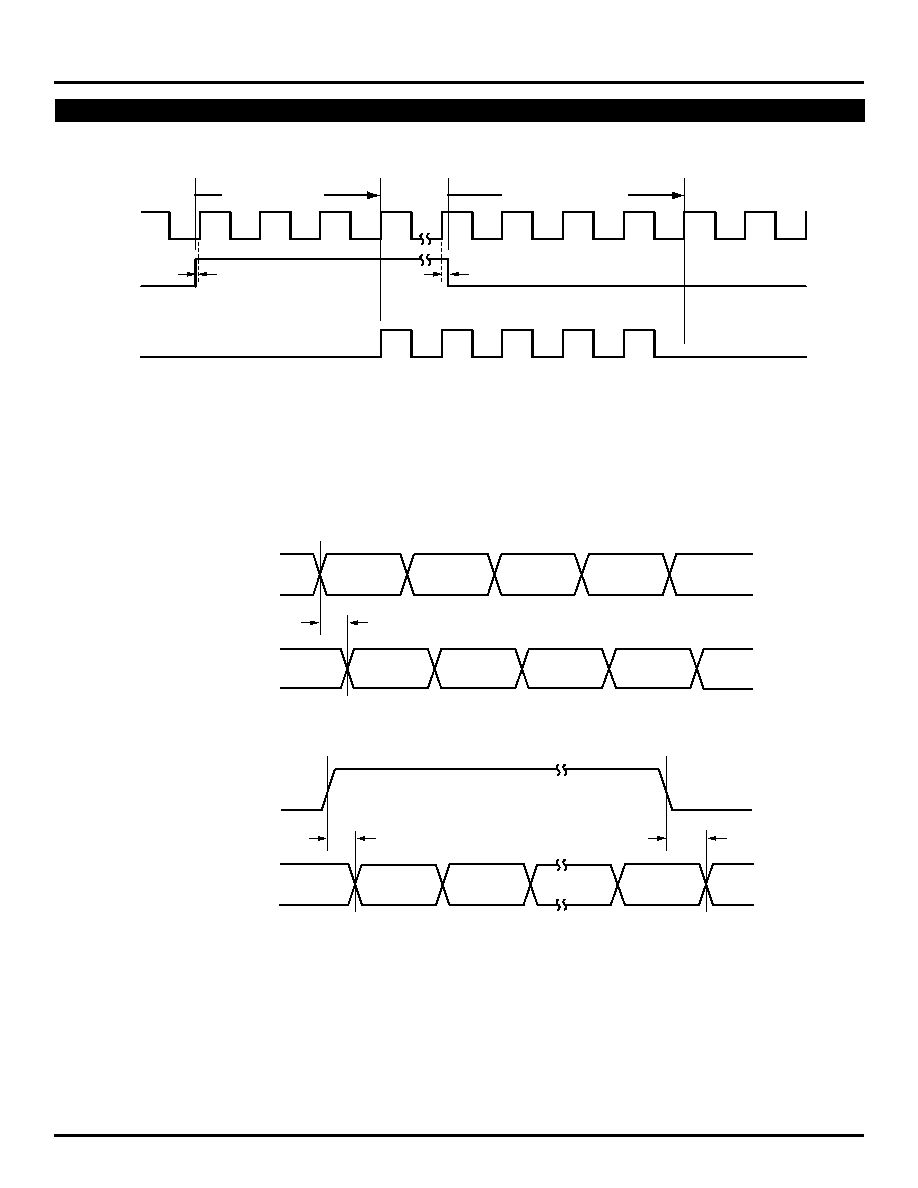
TIMING DIAGRAMS
t
S
t
H
CLK
OE
Q0 - Q21
Assert Latency
De-assert Latency
HSTL_CLK, LVPECL_CLK
/HSTL_CLK, /LVPECL_CLK
Q0 - Q21
/Q0 - /Q21
t
PD
t
PD
CLK_SEL
Q0 - Q21
/Q0 - /Q21
t
PD
Notes:
1. The OE input signal must be a minimum of 3 clock periods with width.
2. The internal enable is asserted and de-asserted on the falling edge of clock.
3. The internal enable occurs 2.5 clock cycles (plus the set-up time of OE with the rising edge of clock) after the rising edge of the external OE.
4. If OE does not meet the t
S
of t
H
specifications as in asynchronous applications, OE must be a minimum of 4 clock periods in width.