 | –≠–ª–µ–∫—Ç—Ä–æ–Ω–Ω—ã–π –∫–æ–º–ø–æ–Ω–µ–Ω—Ç: SY89825U | –°–∫–∞—á–∞—Ç—å:  PDF PDF  ZIP ZIP |
FEATURES
s
LVPECL or LVDS input to 22 LVPECL outputs
s
100K ECL compatible outputs
s
LVDS input includes 100
termination
s
Guaranteed AC parameters over voltage:
∑ > 2GHz f
MAX
(toggle)
∑ < 35ps max. ch-ch skew
s
Low voltage operation: 2.5V, 3.3V
s
Temperature range: ≠40
∞
C to +85
∞
C
s
Output enable pin
s
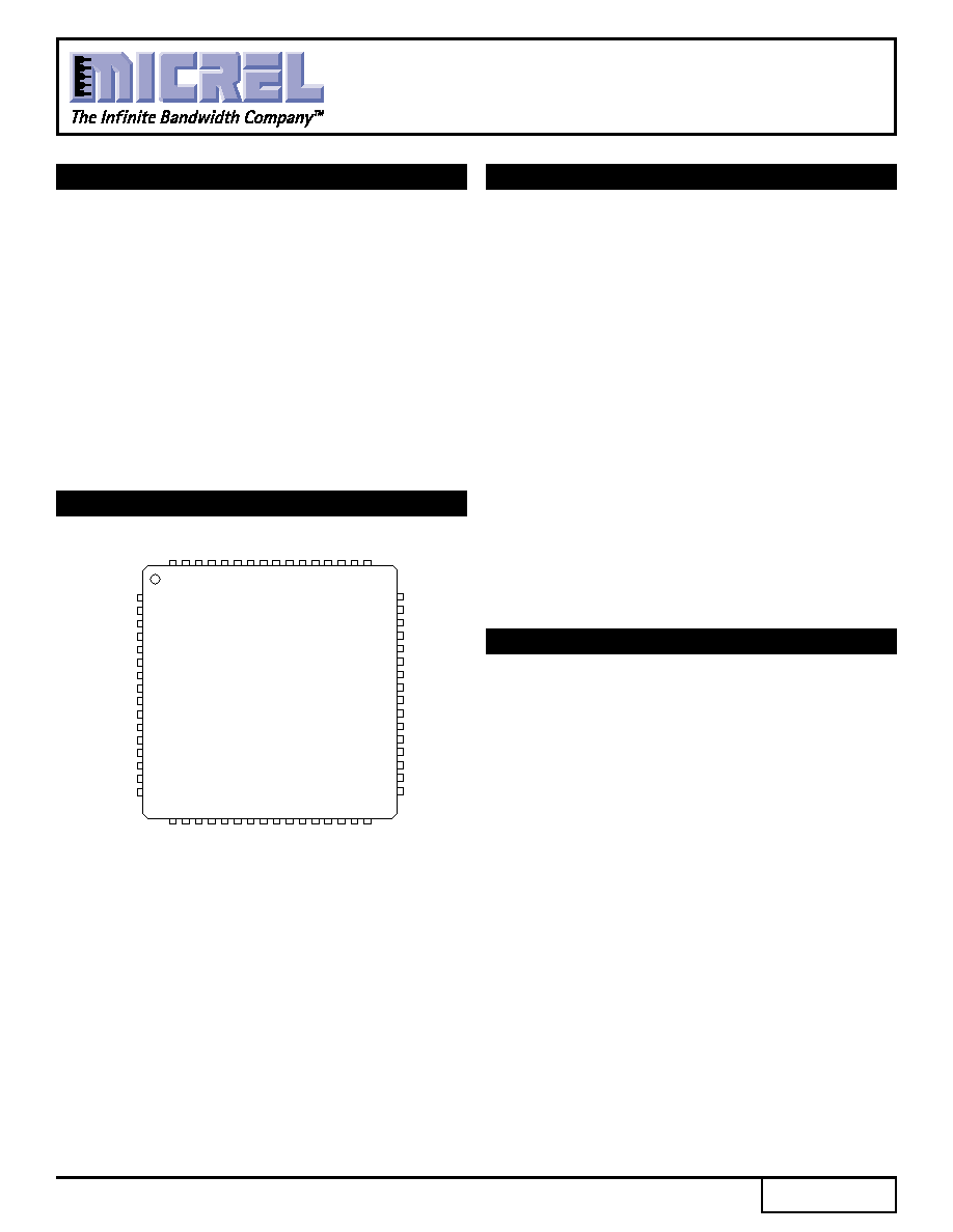
Available in a 64-Pin EPAD-TQFP
The SY89825U is a High Performance Bus Clock Driver
with 22 differential LVPECL output pairs. This part is
designed for use in low voltage (2.5V, 3.3V) applications
which require a large number of outputs to drive precisely
aligned, ultra low skew signals to their destination. The
input is multiplexed from either LVDS or LVPECL by the
CLK_SEL pin. The LVDS input includes a 100
internal
termination, thus eliminating the need for external
termination. The Output Enable (OE) is synchronous so
that the outputs will only be enabled/disabled when they
are already in the LOW state. This eliminates any chance
of generating a runt clock pulse when the device is enabled/
disabled as can happen with an asynchronous control.
The SY89825U features low pin-to-pin skew (35ps max.)
--performance previously unachievable in a standard
product having such a high number of outputs. The
SY89825U is available in a single space saving package
which provides a lower overall cost solution. In addition, a
single chip solution improves timing budgets by eliminating
the multiple device solution with their corresponding large
part-to-part skew.
PIN CONFIGURATION
2.5/3.3V 1:22 HIGH-PERFORMANCE,
LOW-VOLTAGE PECL BUS CLOCK DRIVER
& TRANSLATOR w/ INTERNAL TERMINATION
DESCRIPTION
ClockWorksTM
SY89825U
FINAL
APPLICATIONS
s
High-performance PCs
s
Workstations
s
Parallel processor-based systems
s
Other high-performance computing
s
Communications
1
Rev.: A
Amendment: /0
Issue Date:
September 2001
/Q5
VCCO
Q0
/Q0
Q1
/Q1
Q2
/Q2
Q3
/Q3
Q4
/Q4
Q5
Q6
/Q6
VCCO
VCCO
NC
NC
VCCI
LVDS_CLK
/LVDS_CLK
CLK_SEL
LVPECL_CLK
/LVPECL_CLK
GND
OE
NC
NC
/Q21
Q21
VCCO
VCCO
Q7
/Q7
Q8
/Q8
Q9
/Q9
Q10
/Q10
Q11
/Q11
Q12
/Q12
Q13
/Q13
VCCO
64
1
2
3
4
5
6
7
8
9
10
11
12
13
14
15
16
48
47
46
45
44
43
42
41
40
39
38
37
36
35
34
33
63 62 61 60 59 58 57 56 55 54 53 52 51 50 49
17 18 19 20 21 22 23 24 25 26 27 28 29 30 31 32
64-Pin
EPAD-TQFP
(Top View)
/Q19
VCCO
Q14
/Q14
Q15
/Q15
Q16
/Q16
Q17
/Q17
Q18
/Q18
Q19
Q20
/Q20
VCCO
2
ClockWorksTM
SY89825U
Micrel
LOGIC SYMBOL
CLK_SEL
LVDS_CLK
/LVDS_CLK
LVPECL_CLK
/LVPECL_CLK
OE
0
1
22
22
Q0 - Q21
/Q0 - /Q21
LEN
D
Q
Pin
Function
LVDS_CLK,
Differential LVDS Inputs
/LVDS_CLK
(Internal 100
termination included)
LVPECL_CLK,
Differential LVPECL Inputs.
/LVPECL_CLK
CLK_SEL
Input CLK Select (LVTTL)
OE
Output Enable (LVTTL)
Q
0
≠ Q
21
, /Q
0
≠ /Q
21
Differential LVPECL Outputs.
Terminate with 50
to V
CC
-2V
GND
Ground
V
CCI
Power Supply. Connect to
V
CC
on PCB. V
CCI
and V
CCO
are not
internally connected
V
CCO
Power Supply for Output Buffer.
Connect to V
CCI
on PCB. V
CCI
and
V
CCO
are not internally connected
PIN NAMES
OE
(1)
CLK_SEL
Q
0
≠ Q
21
/Q
0
≠ /Q
21
0
0
LOW
HIGH
0
1
LOW
HIGH
1
0
LVDS_CLK
/LVDS_CLK
1
1
LVPECL_CLK
/LVPECL_CLK
TRUTH TABLE
NOTE:
1. The OE (output enable) signal is synchronized with the low level of the
LVDS_CLK and LVPECL_CLK signal.
Signal
I/O
Level
LVDS_CLK, /LVDS_CLK
Input
LVDS
Q
0
≠ Q
21
, /Q
0
≠ /Q
21
Output
LVPECL
LVPECL_CLK, /LVPECL_CLK
Input
LVPECL
CLK_SEL, OE
Input
LVCMOS/LVTTL
SIGNAL GROUPS
ABSOLUTE MAXIMUM RATINGS
(1)
NOTE:
1. Permanent device damage may occur if ABSOLUTE MAXIMUM RATINGS are exceeded. This is a stress rating only and functional operation is not
implied at conditions other than those detailed in the operational sections of this data book. Exposure to ABSOLUTE MAXIMUM RATING conditions
for extended periods may affect device reliability.
Symbol
Rating
Value
Unit
V
CCI
/ V
CCO
V
CC
Pin Potential to Ground Pin
≠0.5 to +4.0
V
V
IN
Input Voltage
≠0.5 to V
CCI
V
I
OUT
DC Output Current
≠50
mA
Tstore
Storage Temperature
≠65 to +150
∞
C
JA
Package Thermal Resistance (Junction-to-Ambient)
With exposed pad soldered to GND
≠ Still-Air (multi-layer PCB)
23
∞
C/W
≠ 200lfpm (multi-layer PCB)
18
∞
C/W
≠ 500lfpm (multi-layer PCB)
15
∞
C/W
Exposed pad
not soldered to GND
≠ Still-Air (multi-layer PCB)
44
∞
C/W
≠ 200lfpm (multi-layer PCB)
36
∞
C/W
≠ 500lfpm (multi-layer PCB)
30
∞
C/W
JC
Package Thermal Resistance
4.3
∞
C/W
(Junction-to-Case)
3
ClockWorksTM
SY89825U
Micrel
DC ELECTRICAL CHARACTERISTICS
T
A
= ≠40
∞
C
T
A
= +25
∞
C
T
A
= +85
∞
C
Symbol
Parameter
Min.
Typ.
Max.
Min.
Typ.
Max.
Min.
Typ.
Max.
Unit
V
IN
Input Voltage Range
0
--
2.4
0
--
2.4
0
--
2.4
V
V
ID
Differential Input Swing
100
--
--
100
--
--
100
--
--
mV
I
IL
Input Low Current
(1)
≠1.25
--
--
≠1.25
--
--
≠1.25
--
--
mA
R
IN
LVDS Differential Input Resistance
80
100
120
80
100
120
80
100
120
(LVDS_CLK to /LVDS_CLK)
LVDS Input (V
CC
= 2.37V to 3.6V, GND = 0V)
T
A
= ≠40
∞
C
T
A
= +25
∞
C
T
A
= +85
∞
C
Symbol
Parameter
Min.
Typ.
Max.
Min.
Typ.
Max.
Min.
Typ.
Max.
Unit
V
CCI,
Power Supply
(1)
2.37
--
3.6
2.37
--
3.8
2.37
--
3.6
V
V
CCO
I
CC
Total Supply Current
(2)
--
100
150
--
100
150
--
100
150
mA
Power Supply
T
A
= ≠40
∞
C
T
A
= +25
∞
C
T
A
= +85
∞
C
Symbol
Parameter
Min.
Max.
Min.
Max.
Min.
Max.
Unit
V
IH
Input HIGH Voltage
V
CC
≠ 1.165
V
CC
≠ 0.88
V
CC
≠ 1.165
V
CC
≠ 0.88
V
CC
≠ 1.165
V
CC
≠ 0.88
V
(Single ended)
V
IL
Input LOW Voltage
V
CC
≠ 1.945
V
CC
≠ 1.625
V
CC
≠ 1.945
V
CC
≠ 1.625
V
CC
≠ 1.945
V
CC
≠ 1.625
V
V
PP
Minimum Input Swing
(1)
600
--
600
--
600
--
mV
LVPECL_CLK
V
CMR
Common Mode Range
(2)
≠1.5
≠0.4
≠1.5
≠0.4
≠1.5
≠0.4
V
LVPECL_CLK
V
OH
Output HIGH Voltage
(3)
V
CCO
≠ 1.085 V
CCO
≠ 0.880 V
CCO
≠ 1.025 V
CCO
≠ 0.880 V
CCO
≠ 1.025 V
CCO
≠ 0.880
V
V
OL
Output LOW Voltage
(3)
V
CCO
≠ 1.830 V
CCO
≠ 1.555 V
CCO
≠ 1.810 V
CCO
≠ 1.620 V
CCO
≠ 1.810 V
CCO
≠ 1.620
V
I
IH
Input HIGH Current
--
150
--
150
--
150
µ
A
I
IL
Input LOW Current
0.5
--
0.5
--
0.5
--
µ
A
LVPECL Input/Output (V
CC
= 2.37V to 3.6V, GND = 0V)
NOTES:
1. The V
PP
(min.) is defined as the minimum input differential voltage which will cause no increase in the propagation delay.
2. V
CMR
is defined as the range within which the V
IH
level may vary, with the device still meeting the propagation delay specification. The numbers in the table are
referenced to V
CCI
. The V
IL
level must be such that the peak-to-peak voltage is less than 1.0V and greater than or equal to V
PP
(min.). The lower end of the
CMR range varies 1:1 with V
CCI
. The V
CMR
(min) will be fixed at 3.3V ≠ |V
CMR
(min)|.
3. Outputs loaded with 50
to V
CC
-2V.
NOTES:
1. V
CCI
and V
CCO
must be connected together on the PCB such that they remain at the same potential. V
CCI
and V
CCO
are not internally connected on the die.
2. No load. Outputs floating.
T
A
= ≠40
∞
C
T
A
= +25
∞
C
T
A
= +85
∞
C
Symbol
Parameter
Min.
Typ.
Max.
Min.
Typ.
Max.
Min.
Typ.
Max.
Unit
V
IH
Input HIGH Voltage
2.0
--
--
2.0
--
--
2.0
--
--
V
V
IL
Input LOW Voltage
--
--
0.8
--
--
0.8
--
--
0.8
V
I
IH
Input HIGH Current
+20
--
≠250
+20
--
≠250
+20
--
≠250
µ
A
I
IL
Input LOW Current
--
--
≠600
--
--
≠600
--
--
≠600
µ
A
LVCMOS/LVTTL Control Inputs (OE, CLK_SEL) (V
CC
= 2.37V to 3.6V, GND = 0V)
NOTE:
1. For I
IL
, both LVDS inputs are grounded.
4
ClockWorksTM
SY89825U
Micrel
NOTES:
1. Outputs loaded with 50
to V
CC
≠ 2V. Airflow
300lfpm.
2. f
MAX
is defined as the maximum toggle frequency measured. Measured with a 750mV input signal, all loading with 50
to V
CC
≠2V.
3. Differential propagation delay is defined as the delay from the crossing point of the differential input signals to the crossing point of the differential
output signals.
4. The within-device skew is defined as the worst case difference between any two similar delay paths within a single device operating at the same
voltage and temperature.
5. The part-to-part skew is defined as the absolute worst case difference between any two delay paths on any two devices operating at the same
voltage and temperature. Part-to-part skew is the total skew difference; pin-to-pin skew + part-to-part skew.
6. Set-up and hold time applies to synchronous applications that intend to enable/disable before the next clock cycle. For asynchronous applications,
set-up and hold time does not apply. OE set-up time is defined with respect to the rising edge of the clock. OE HIGH to LOW transition ensures
outputs remain disabled during the next clock cycle. OE LOW to HIGH transition enables normal operation of the next input clock.
AC ELECTRICAL CHARACTERISTICS
(1)
T
A
= ≠40
∞
C
T
A
= +25
∞
C
T
A
= +85
∞
C
Symbol
Parameter
Min.
Typ.
Max.
Min.
Typ.
Max.
Min.
Typ.
Max.
Unit
f
MAX
Max Toggle Frequency
(2)
2
--
--
2
--
--
2
--
--
GHz
t
PHL
Propagation Delay
ns
t
PLH
(Differential)
(3)
LVPECL IN
0.600
--
1.2
0.600
0.900
1.2
0.600
--
1.2
LVDS IN
0.800
--
1.4
0.800
1.1
1.4
0.800
--
1.4
t
SKEW
Within-Device Skew
(4)
--
--
35
--
20
35
--
--
35
ps
Part-to-Part Skew
(5)
--
100
200
--
100
200
--
100
200
ps
t
S(OE)
OE Set-Up Time
(6)
1.0
--
--
1.0
--
--
1.0
--
--
ns
t
H(OE)
OE Hold Time
(6)
0.5
--
--
0.5
--
--
0.5
--
--
ns
t
r
Output Rise/Fall Time
300
--
600
300
450
600
300
--
600
ps
t
f
(20% ≠ 80%)
t
(switchover)
Input Switchover
--
--
1.2
--
--
1.2
--
--
1.2
ns
CLK_SEL-to-valid output
PRODUCT ORDERING CODE
Ordering
Package
Operating
Package
Code
Type
Range
Marking
SY89825UHI
H64-1
Industrial
SY89825UHI
V
CC
= 2.37V to 3.6V, GND = 0V
5
ClockWorksTM
SY89825U
Micrel
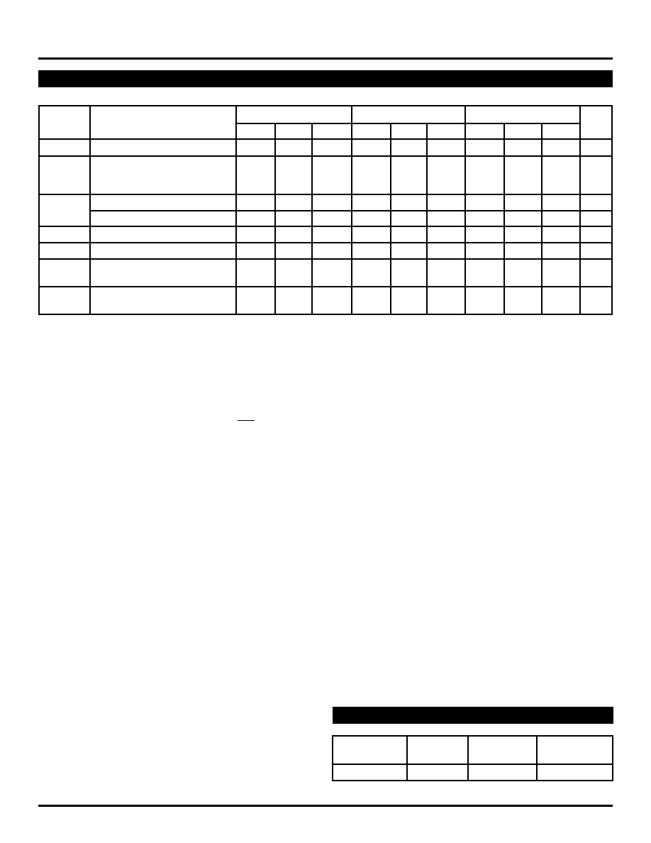
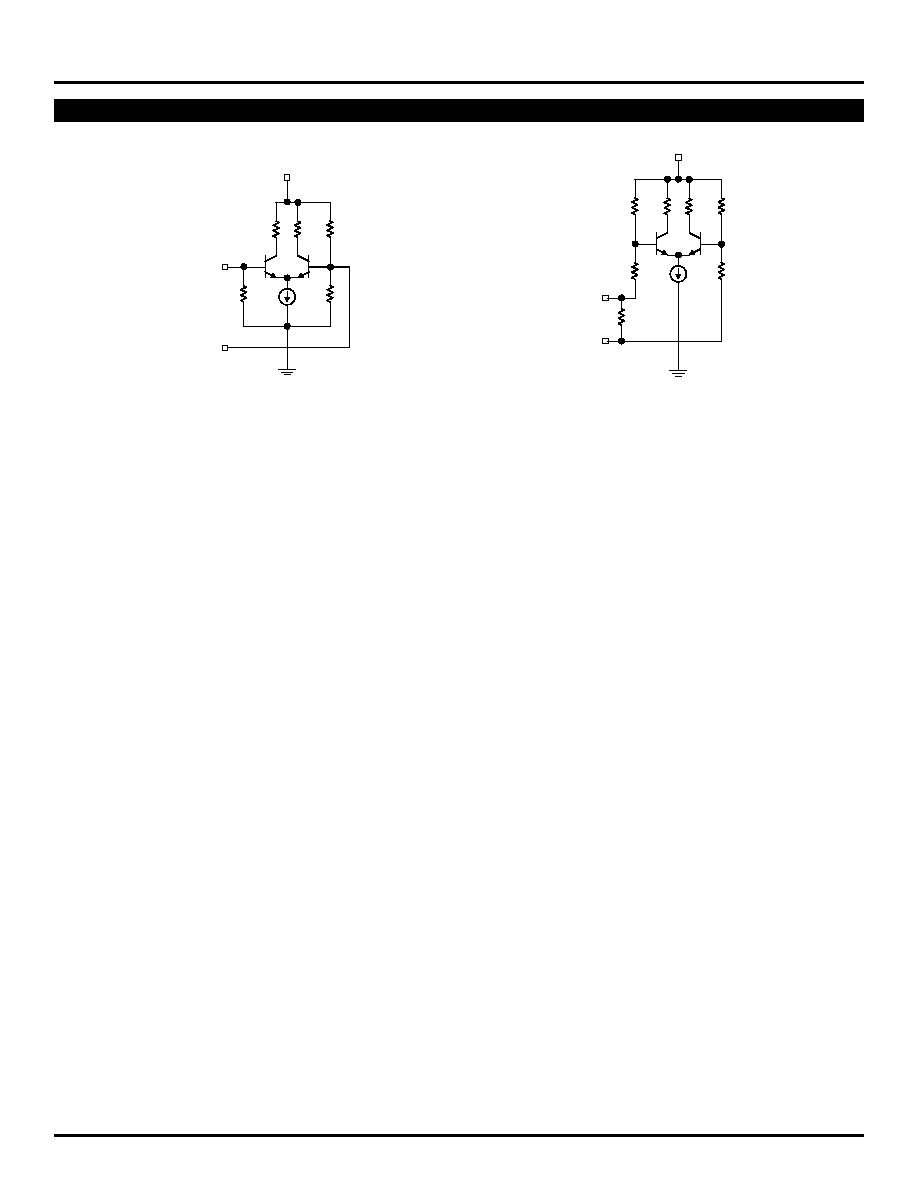
75k
75k
75k
GND
LVPECL_CLK
V
CC
/LVPECL_CLK
LVPECL Input Stage
Figure 1. Simplified LVPECL & LVDS Input Stage
1.9k
1.9k
1.9k
GND
V
CC
V
IN
V
IN
1.9k
100
LVDS Input Stage
LVDS/LVPECL INPUTS