DESCRIPTION
s
High-performance, 1GHz LVDS fanout buffer/
translator
s
22 differential LVDS output pairs
s
Guaranteed AC parameters over temperature and
voltage:
∑ > 1GHz f
MAX
∑ < 50ps within device skew
∑ < 400ps t
r
/ t
f
time
s
Low jitter performance
∑ < 1ps (rms) cycle-to-cycle jitter
∑ < 1ps (pk-pk) total jitter
s
2:1 mux input accepts LVDS and LVPECL
3.3V supply voltage
s
LVDS input includes internal 100
termination
s
Output enable function
s
Available in a 64-Pin EPAD-TQFP
FEATURES
3.3V 1GHz PRECISION 1:22 LVDS
FANOUT BUFFER/TRANSLATOR
WITH 2:1 INPUT MUX
SY89826L
Final
APPLICATIONS
s
Enterprise networking
s
High-end servers
s
Communications
1
Rev.: A
Amendment: /0
Issue Date:
August 2002
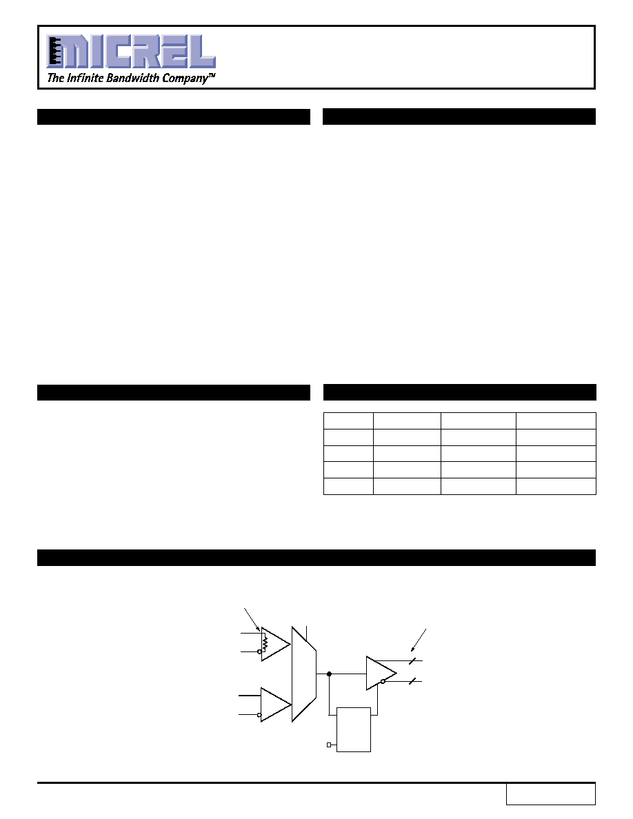
The SY89826L is a precision fanout buffer with 22
differential LVDS (Low Voltage Differential Swing) output
pairs. The part is designed for use in low voltage 3.3V
applications that require a large number of outputs to drive
precisely aligned, ultra low-skew signals to their destination.
The input is multiplexed from either LVDS or LVPECL (Low
Voltage Positive Emitter Coupled Logic) by the CLK_SEL
pin. The OE (Output Enable) is synchronous so that the
outputs will only be enabled/disabled when they are already
in the LOW state. This avoids any chance of generating a
runt clock pulse when the device is enabled/disabled as
can happen with an asynchronous control.
The SY89826L features a low pin-to-pin skew of less
than 50ps--performance previously unachievable in a
standard product having such a high number of outputs.
The SY89826L is available in a single space saving package,
enabling a lower overall cost solution.
OE
(1)
CLK_SEL
Q0 ≠ Q21
/Q0 ≠ /Q21
0
0
LOW
HIGH
0
1
LOW
HIGH
1
0
LVDS_CLK
/LVDS_CLK
1
1
LVPECL_CLK
/LVPECL_CLK
TRUTH TABLE
NOTE:
1. The OE (output enable) signal is synchronized with the low level of the
LVDS_CLK and LVPECL_CLK signal.
FUNCTIONAL BLOCK DIAGRAM
CLK_SEL
LVPECL_CLK
/LVPECL_CLK
OE
0
1
22
22
Q0 - Q21
/Q0 - /Q21
LEN
D
Q
LVDS_CLK
/LVDS_CLK
100
internal input
termination
22 LVDS compatible
outputs
2
SY89826L
Micrel
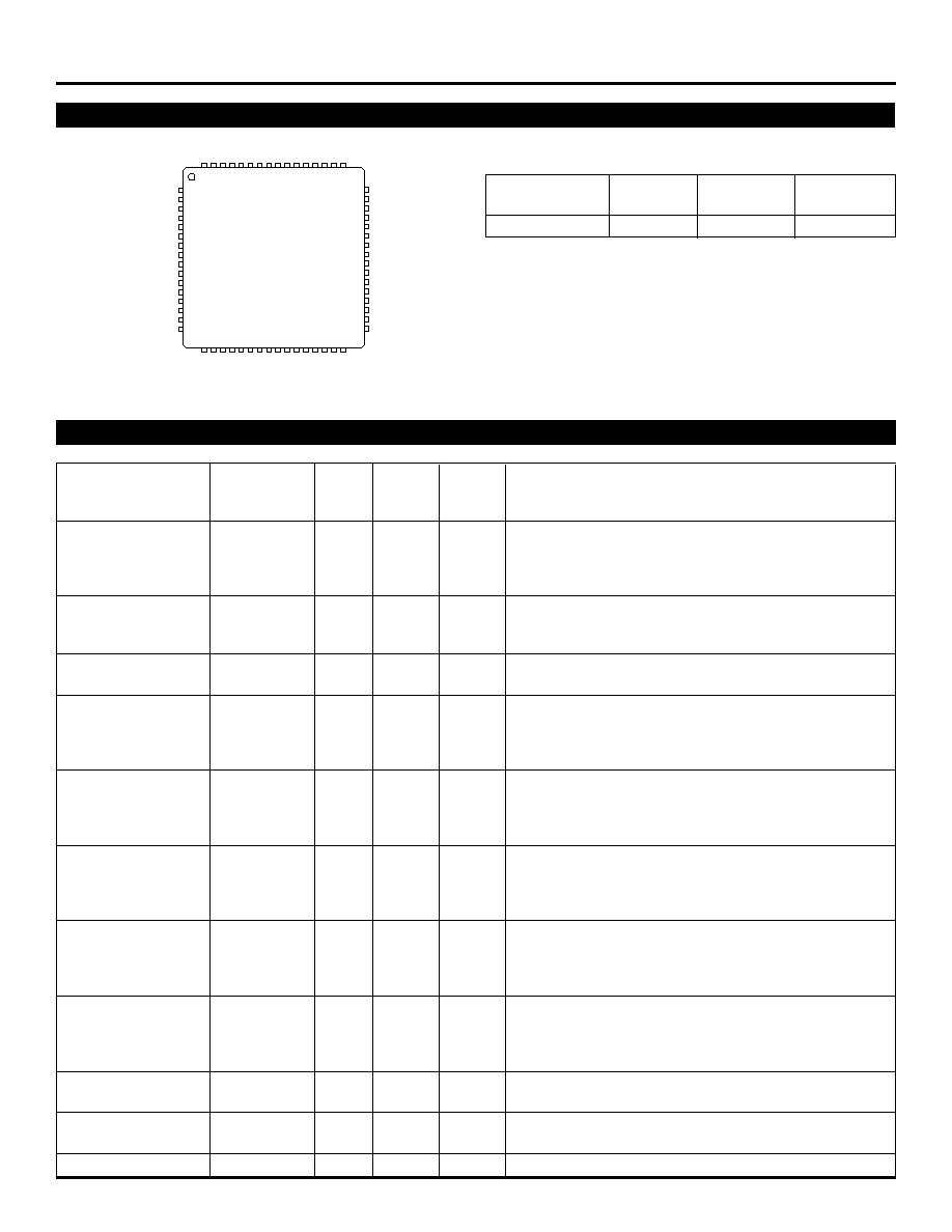
PACKAGE/ORDERING INFORMATION
Ordering Information
Package
Operating
Package
Part Number
Type
Range
Marking
SY89826LHI
H64-1
Industrial
SY89826L
Q1
VCCO
/Q6
Q6
/Q5
Q5
/Q4
Q4
/Q3
Q3
/Q2
Q2
/Q1
/Q0
Q0
VCCO
VCCO
GNDO
NC
VCCI
LVDS_CLK
/LVDS_CLK
CLK_SEL
LVPECL_CLK
/LVPECL_CLK
GNDI
OE
NC
GNDO
/Q21
Q21
VCCO
GNDO
Q7
/Q7
Q8
/Q8
Q9
/Q9
Q10
/Q10
Q11
/Q11
Q12
/Q12
Q13
/Q13
GNDO
64
1
2
3
4
5
6
7
8
9
10
11
12
13
14
15
16
48
47
46
45
44
43
42
41
40
39
38
37
36
35
34
33
63 62 61 60 59 58 57 56 55 54 53 52 51 50 49
17 18 19 20 21 22 23 24 25 26 27 28 29 30 31 32
/Q19
VCCO
Q14
/Q14
Q15
/Q15
Q16
/Q16
Q17
/Q17
Q18
/Q18
Q19
Q20
/Q20
VCCO
64-Pin TQFP (H64-1)
PIN DESCRIPTIONS
Internal
Pull-up/
Pin Number
Pin Name
I/O
Type
Pull-down Pin Function
5, 6
LVDS_CLK
Input
LVDS
3.3k
Differential LVDS clock input. Selected when CLKSEL = LOW
/LVDS_CLK
w/100
pull-up
(Can be left floating if CLKSEL = HIGH). This input pair
internal (Figure 2) includes internal termination, and is intended to interface
terminator
directly to LVDS. Leave floating if not used.
8, 9
LVPECL_CLK
Input
LVPECL
75k
Differential LVPECL clock input. Selected when CLKSEL =
/LVPECL_CLK
pull-down HIGH (Can be left floating if CLKSEL = LOW). Requires
(Figure 1) external termination. Leave floating if not used.
7
CLK_SEL
Input
LVTTL/
11k
to
Selects LVDS_CLK when LOW and LVPECL_CLK when
CMOS
VCCI
HIGH. Default condition is HIGH if left floating.
11
OE
Input
LVTTL/
Output enable/disable function. When LOW, Q outputs go
LOW, /Q outputs go HIGH. Asynchronous input that is
synchronized internally to prevent output glitches or runt
pulses.
63, 61, 59, 57, 55, 53,
Q0 ≠ Q21
Output
LVDS
Differential LVDS clock outputs when OE = HIGH and static
51, 47, 45, 43, 41, 39,
LOW when OE = LOW. Unused output pairs must be
37, 35, 31, 29, 27, 25,
terminated with 100
across the differential pair to maintain
23, 21, 19, 15
low skew and jitter.
62, 60, 58, 56, 54, 52,
/Q0 ≠ /Q21
Output
LVDS
Differential clock outputs (complement) when OE = HIGH
50, 46, 44, 42, 40, 38,
and static HIGH when OE = LOW. Unused output pairs
36, 34, 30, 28, 26, 24,
must be terminated with 100
across the differential pair to
22, 20, 18, 14
maintain low skew and jitter.
4
VCCI
Power
Core VCC connect to 3.3V supply. Not connected to
VCCO internally. Connect to VCCO on PCB. Bypass
with 0.1
µ
F in parallel with 0.01
µ
F low ESR capacitors as
close to VCC pins as possible.
1, 16, 17,
VCCO
Power
Output buffer VCC connects to 3.3V supply. Not connected
32, 49, 64
to VCCI internally. Connect to VCCI on PCB. Bypass
with 0.1
µ
F in parallel with 0.01
µ
F low ESR capacitors as
close to VCC pins as possible.
10
GNDI
Power
Core ground not connected to GNDO internally.
Connect to GNDO on PCB.
2, 13, 33, 48
GNDO
Power
Output buffer ground not connected to GNDI internally.
Connect to GNDI on PCB.
3, 12
NC
No connect pins to be left open.
3
SY89826L
Micrel
Absolute Maximum Ratings
(Note 1)
Power Supply Voltage (V
CCI
,
V
CCO
) .............. ≠0.5 to +4.0V
Input Voltage (V
IN
) ........................................... ≠0.5 to V
CCI
Output Current (I
OUT
) ...............................................
±
10mA
Storage Temperature (T
S
) ........................... ≠65 to +150
∞
C
ESD Rating, Note 3 .................................................... >1kV
Operating Ratings
(Note 2)
Supply Voltage (V
CC
to GND) ..................... +3.0V to +3.6V
Ambient Temperature (T
A
) ......................... ≠40
∞
C to +85
∞
C
Package Thermal Resistance
TQFP
(
JA
)
Exposed pad soldered to GND
Still-Air(multi-layer PCB) .................................. 23
∞
C/W
≠200lfpm (multi-layer PCB) ............................. 18
∞
C/W
≠500lfpm (multi-layer PCB) ............................. 15
∞
C/W
Exposed pad NOT soldered to GND (not recommened)
Still-Air(multi-layer PCB) .................................. 44
∞
C/W
≠200lfpm (multi-layer PCB) ............................. 36
∞
C/W
≠500lfpm (multi-layer PCB) ............................. 30
∞
C/W
TQFP
(
JC
) ......................................................... 4.4
∞
C/W
Power Supply
: T
A
= ≠40
∞
C to +85
∞
C
Symbol
Parameter
Condition
Min
Typ
Max
Units
V
CCI
, V
CCO
V
CC
Core, V
CC
Output
Note 4
3.0
3.3
3.6
V
I
CCI
I
CC
Core
Max. V
CC
46
70
mA
I
CCO
I
CC
Output
No Load, Max. V
CC
175
260
mA
Note 4.
V
CCI
and V
CCO
must be connected together on the PCB such that they remain at the same potential. V
CCI
and V
CCO
are not internally
connected on the die.
LVDS Input
: V
CC
= 3.3V
±
10%, T
A
= ≠40
∞
C to +85
∞
C
Symbol
Parameter
Condition
Min
Typ
Max
Units
V
IN
Input Voltage Range
0
2.4
V
V
ID
Differential Input Swing
100
mV
I
IL
Input LOW Current
≠1.25
mA
R
IN
LVDS Differential Input Resistance
80
100
120
(LVDS_CLK to /LVDS_CLK)
DC ELECTRICAL CHARACTERISTICS
Note 1.
Permanent device damage may occur if ABSOLUTE MAXIMUM RATINGS are exceeded. This is a stress rating only and functional
operation is not implied at conditions other than those detailed in the operational sections of this data sheet. Exposure to ABSOLUTE
MAXIMUM RATlNG conditions for extended periods may affect device reliability.
Note 2.
The data sheet limits are not guaranteed if the device is operated beyond the operating ratings.
Note 3.
Devices are ESD sensitive. Handling precautions recommended.
4
SY89826L
Micrel
LVPECL Input:
V
CC
= 3.3V
±
10%, T
A
= ≠40
∞
C to +85
∞
C
Symbol
Parameter
Condition
Min
Typ
Max
Units
V
IH
Input HIGH Voltage (Single-Ended)
V
CC
≠1.165
V
CC
≠0.880
V
V
IL
Input LOW Voltage
V
CC
≠1.945
V
CC
≠1.625
V
V
PP
Minimum Input Swing (LVPECL_CLK)
Note 6
300
mV
V
CMR
Common Mode Range (LVPECL_CLK)
Note 7
GNDI +1.8
V
CCI
≠0.4
V
I
IH
Input HIGH Current
150
µ
A
I
IL
Input LOW Current
0.5
µ
A
Note 6.
The V
PP
(min.) is defined as the minimum input differential voltage which will cause no increase in the propagation delay.
Note 7.
V
CMR
is defined as the range within which the V
IH
level may vary, with the device still meeting the propagation delay specification. The
numbers in the table are referenced to V
CCI
. The V
IL
level must be such that the peak-to-peak voltage is less than 1.0V and greater than or
equal to V
PP
(min.). V
CMR
range varies 1:1 with V
CCI
. V
CMR
(min) is fixed at GNDI +1.8V.
CMOS/LVTTL Inputs:
V
CC
= 3.3V
±
10%, T
A
= ≠40
∞
C to +85
∞
C
Symbol
Parameter
Condition
Min
Typ
Max
Units
V
IH
Input HIGH Voltage
2.0
V
V
IL
Input LOW Voltage
0.8
V
I
IH
Input HIGH Current
V
IN
=
V
CC
150
µ
A
I
IL
Input LOW Current
V
IN
=
0.5V
≠600
µ
A
LVDS Output
:
V
CC
= 3.3V
±
10%, T
A
= ≠40
∞
C to +85
∞
C
Symbol
Parameter
Condition
Min
Typ
Max
Units
V
OD
Differential Output Voltage
Note 8, 9
250
350
400
mV
V
OH
Output HIGH Voltage
Note 8
1.474
V
V
OL
Output LOW Voltage
Note 8
0.925
V
V
OCM
Output Common Mode Voltage
Note 9
1.125
1.375
V
V
OCM
Change in Common Mode Voltage
≠50
50
mV
Note 8.
Measured as per Figure 3, 100
across Q and /Q outputs.
Note 9.
Measured as per Figure 4.
DC ELECTRICAL CHARACTERISTICS
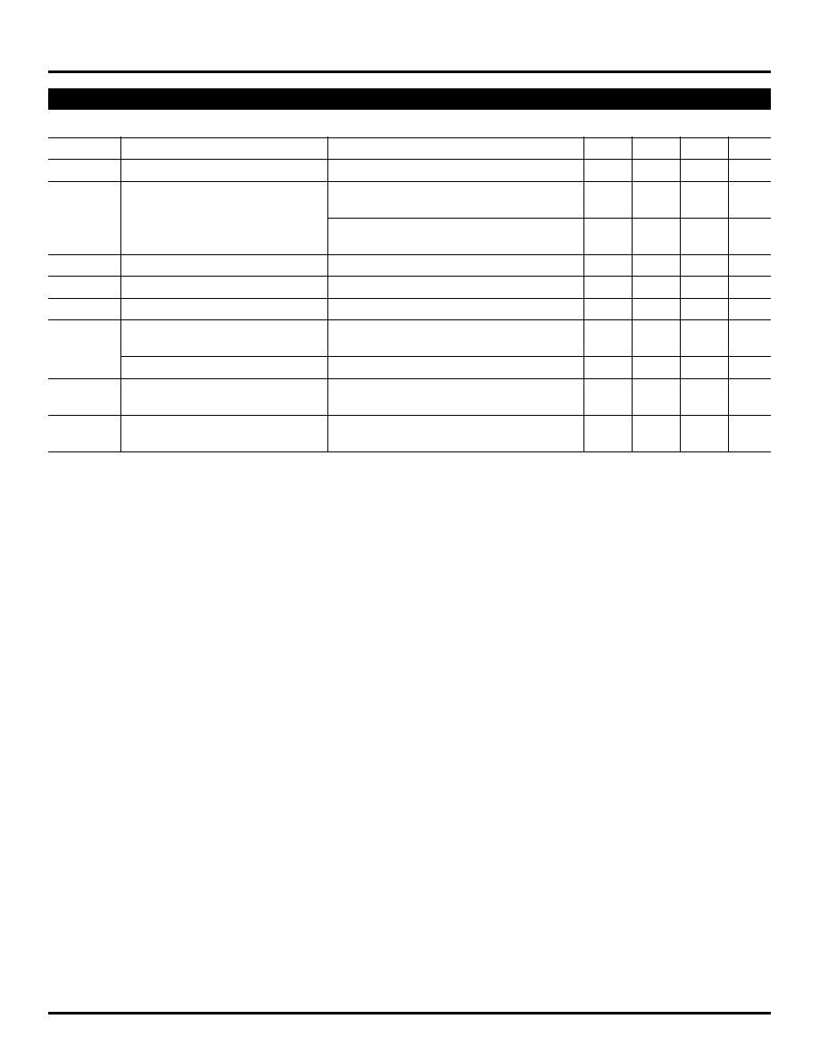
5
SY89826L
Micrel
V
CC
= 3.3V
±
10%, T
A
= ≠40
∞
C to +85
∞
C, unless noted.
Symbol
Parameter
Condition
Min
Typ
Max
Units
f
MAX
Maximum Toggle Frequency
Note 2
1.0
GHz
t
PHL
Differential Propagation Delay,
LVPECL Input: 150mV
0.750
1.0
1.250
ns
t
PLH
Note 3
LVPECL Input: 800mV
0.6
0.850
1.10
ns
LVDS Input: 100mV
0.950
1.2
1.450
ns
LVDS Input: 400mV
0.800
1.0
1.30
ns
t
SWITCHOVER
Clock Input Switchover
CLK_SEL-to-Valid Output
1.4
1.7
ns
t
S(OE)
Output Enable Set-Up Time
Note 4
1.0
ns
t
H(OE)
Output Enable Hold Time
Note 4
0.5
ns
t
skew
Within Device Skew
Note 5
0
∞
C to +85
∞
C
25
50
ps
≠40
∞
C
75
ps
Part-to-Part Skew
Note 6
400
ps
t
JITTER
Cycle-to-Cycle
Note 7
1
ps(rms)
Total Jitter
Note 8
<1
2
ps(pk-pk)
t
r
, t
f
Output Rise/Fall Times
200
290
400
ps
(20% to 80%)
Note 1.
100
termination between Q and /Q outputs. Airflow
300lfpm, or exposed pad soldered to ground plane. Typicals are at nominal supply,
T
A
= 25
∞
C.
Note 2.
f
MAX
is defined as the maximum toggle frequency, measured with a 750mV LVPECL input or 350mV LVDS input. Output swing is
200mV.
Note 3.
Differential propagation delay is defined as the delay from the crossing point of the differential input signals to the crossing point of the differential
output signals.
Note 4.
Set-up and hold time applies to synchronous applications that intend to enable/disable before the next clock cycle. For asynchronous applications,
set-up and hold time does not apply. OE set-up time is defined with respect to the rising edge of the clock. OE HIGH to LOW transition ensures
outputs remain disabled during the next clock cycle. OE LOW to HIGH transition enables normal operation of the next input clock.
Note 5.
The within-device skew is defined as the worst case difference between any two similar delay paths within a single device with identical input
transition, operating at the same voltage and temperature.
Note 6.
The part-to-part skew is defined as the absolute worst case difference between any two delay paths on any two devices operating at the same voltage
and temperature. Part-to-part skew is the total skew difference; pin-to-pin skew + part-to-part skew.
Note 7.
Cycle-to-cycle jitter definition: The variation in period between adjacent cycles over a random sample of adjacent cycle pairs. T
JITTER_CC
=T
n
≠T
n+1
where T is the time between rising edges of the output signal.
Note 8.
Total jitter definition: with an ideal clock input, no more than one output edge in 10
12
output edges will deviate by more than the specified peak-to-
peak jitter value.
AC ELECTRICAL CHARACTERISTICS,
(NOTE 1)