DESCRIPTION
s
Dual LVPECL or HSTL input, 10 differential 1.5V
HSTL compatible outputs
s
Configurable as dual-channel 10 output or a single-
channel 20 output clock driver
s
Guaranteed AC parameters over temperature and
voltage:
∑ > 500MHz f
MAX
∑ < 50ps within device skew
∑ < 1.3ns propagation delay
∑ < 700ps t
r
/ t
f
time
s
Low jitter design
∑ < 1ps (rms) cycle-to-cycle jitter
∑ < 1ps pk-pk total jitter
s
3.3V core supply, 1.8V output supply
s
Output enable function
s
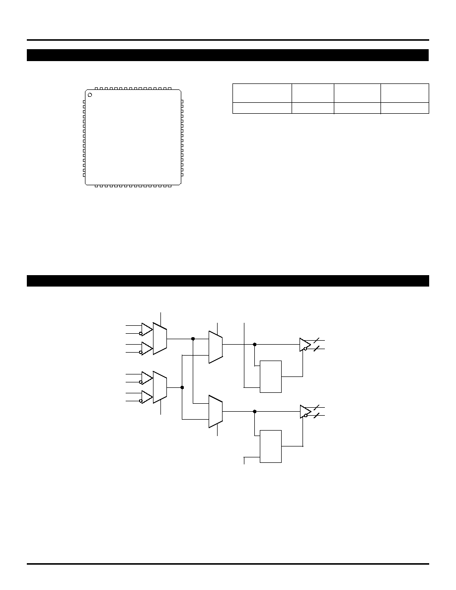
Available in a 64-Pin EPAD-TQFP
FEATURES
3.3V 500MHz DUAL 1:10 HSTL
FANOUT BUFFER/TRANSLATOR
WITH 2:1 MUX INPUT
Precision EdgeTM
SY89827L
FINAL
APPLICATIONS
s
High-performance PCs
s
Workstations
s
Parallel processor-based systems
s
Other high-performance computing
s
Communications
1
Rev.: B
Amendment: /1
Issue Date:
December 2002
The SY89827L is a High Performance Bus Clock Driver
with dual 1:10 or single 1:20 HSTL (High Speed
Transceiver Logic) output pairs. The part is designed for
use in low voltage (3.3V/1.8V) applications which require
a large number of outputs to drive precisely aligned, ultra
low skew signals to their destination. The input is
multiplexed from either HSTL or LVPECL (Low Voltage
Positive Emitter Coupled Logic) by the CLK_SEL pin.
The Output Enables (OE1 & OE2) are synchronous so
that the outputs will only be enabled/disabled when they
are already in the LOW state. This avoids any chance of
generating a runt clock pulse when the device is enabled/
disabled as can happen with an asynchronous control.
The SY89827L features extremely low skew
performance of <50ps over temperature and voltage≠
performance previously unachievable in a standard
product having such a high number of outputs. The
SY89827L is available in a single space saving package,
enabling a lower overall cost solution. For applications
that require greater HSTL fanout capability, consider the
SY89824L.
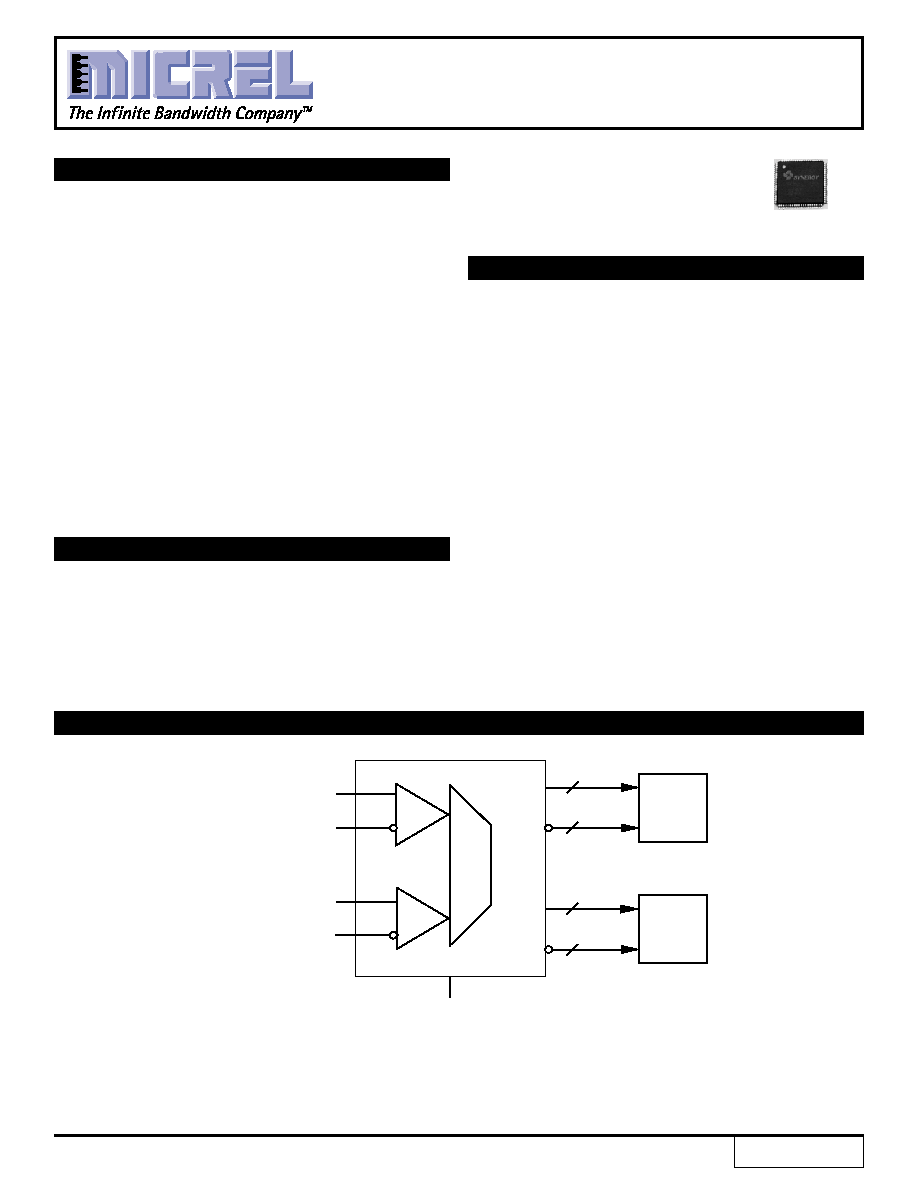
TYPICAL APPLICATION CIRCUIT
SEL1
Primary/Backup Clock Select
(Switchover within 2.0ns)
LVPECL_CLKA
/LVPECL_CLKA
LVPECL_CLKB
/LVPECL_CLKB
Primary Clock Source
Redundant Backup
Clock Source
10
10
10
10
Primary
Card
Redundant
Card
System using SY89827L as a switchover circuit from a Primary Clock to a Redundant Backup Clock in a failsafe application.
LVPECL inputs only, shown in this application.
Precision Edge is a trademark of Micrel, Inc.
Precision EdgeTM
2
Precision EdgeTM
SY89827L
Micrel
PACKAGE/ORDERING INFORMATION
Ordering Information
Package
Operating
Package
Part Number
Type
Range
Marking
SY89827LHI
H64-1
Industrial
SY89827L
Q1
VCCO
/Q6
Q6
/Q5
Q5
/Q4
Q4
/Q3
Q3
/Q2
Q2
/Q1
/Q0
Q0
VCCO
SEL2
HSTL_CLKB
/HSTL_CLKB
VCCI
HSTL_CLKA
/HSTL_CLKA
CLK_SEL1
LVPECL_CLKA
/LVPECL_CLKA
GND
OE1
LVPECL_CLKB
/LVPECL_CLKB
CLK_SEL2
OE2
SEL1
VCCO
Q7
/Q7
Q8
/Q8
Q9
/Q9
VCCO
VCCO
Q10
/Q10
Q11
/Q11
Q12
/Q12
VCCO
64
1
2
3
4
5
6
7
8
9
10
11
12
13
14
15
16
48
47
46
45
44
43
42
41
40
39
38
37
36
35
34
33
63 62 61 60 59 58 57 56 55 54 53 52 51 50 49
17 18 19 20 21 22 23 24 25 26 27 28 29 30 31 32
/Q18
VCCO
Q13
/Q13
Q14
/Q14
Q15
/Q15
Q16
/Q16
Q17
/Q17
Q18
Q19
/Q19
VCCO
64-Pin TQFP (H64-1)
FUNCTIONAL BLOCK DIAGRAM
0
1
HSTL_CLKA
/HSTL_CLKA
LVPECL_CLKA
/LVPECL_CLKA
HSTL_CLKB
/HSTL_CLKB
LVPECL_CLKB
/LVPECL_CLKB
CLK_SEL2
0
1
SEL2
SEL1
0
1
OE2
OE1
0
1
Q
0
≠ Q
9
10
10
/Q
0
≠ /Q
9
Q
10
≠ Q
19
10
10
/Q
10
≠ /Q
19
LEN
D
Q
CLK_SEL1
LEN
D
Q
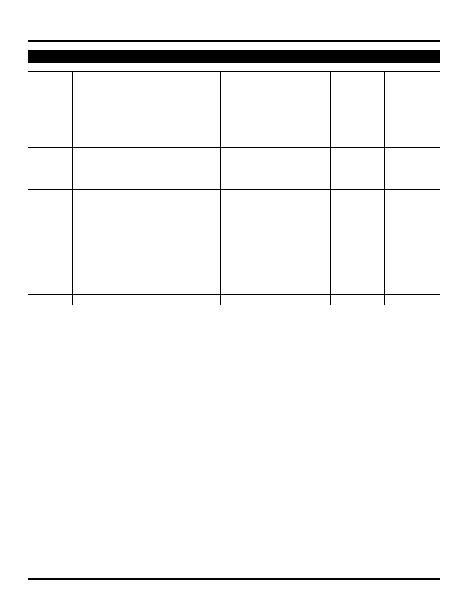
3
Precision EdgeTM
SY89827L
Micrel
OE1
(1)
OE2
(1)
SEL1
(1)
SEL2
(1)
CLK_SEL1
(1)
CLK_SEL2
(1)
Q0 ≠ Q9
/Q0 ≠ /Q9
Q10 ≠ Q19
/Q10 ≠ /Q19
1
1
0
0
0
X
HSTL_CLKA
/HSTL_CLKA
HSTL_CLKA
/HSTL_CLKA
1
1
0
0
1
X
LVPECL_CLKA
/LVPECL_CLKA
LVPECL_CLKA
/LVPECL_CLKA
1
1
0
1
0
0
HSTL_CLKA
/HSTL_CLKA
HSTL_CLKB
/HSTL_CLKB
1
1
0
1
0
1
HSTL_CLKA
/HSTL_CLKA
LVPECL_CLKB
/LVPECL_CLKB
1
1
0
1
1
0
LVPECL_CLKA
/LVPECL_CLKA
HSTL_CLKB
/HSTL_CLKB
1
1
0
1
1
1
LVPECL_CLKA
/LVPECL_CLKA
LVPECL_CLKB
/LVPECL_CLKB
1
1
1
0
0
0
HSTL_CLKB
/HSTL_CLKB
HSTL_CLKA
/HSTL_CLKA
1
1
1
0
0
1
LVPECL_CLKB
/LVPECL_CLKB
HSTL_CLKA
/HSTL_CLKA
1
1
1
0
1
0
HSTL_CLKB
/HSTL_CLKB
LVPECL_CLKA
/LVPECL_CLKA
1
1
1
0
1
1
LVPECL_CLKB
/LVPECL_CLKB
LVPECL_CLKA
/LVPECL_CLKA
1
1
1
1
X
0
HSTL_CLKB
/HSTL_CLKB
HSTL_CLKB
/HSTL_CLKB
1
1
1
1
X
1
LVPECL_CLKB
/LVPECL_CLKB
LVPECL_CLKB
/LVPECL_CLKB
0
1
X
0
0
X
LOW
HIGH
HSTL_CLKA
/HSTL_CLKA
0
1
X
0
1
X
LOW
HIGH
LVPECL_CLKA
/LVPECL_CLKA
0
1
X
1
X
0
LOW
HIGH
HSTL_CLKB
/HSTL_CLKB
0
1
X
1
X
1
LOW
HIGH
LVPECL_CLKB
/LVPECL_CLKB
1
0
0
X
0
X
HSTL_CLKA
/HSTL_CLKA
LOW
HIGH
1
0
0
X
1
X
LVPECL_CLKA
/LVPECL_CLKA
LOW
HIGH
1
0
1
X
X
0
HSTL_CLKB
/HSTL_CLKB
LOW
HIGH
1
0
1
X
X
1
LVPECL_CLKB
/LVPECL_CLKB
LOW
HIGH
0
0
X
X
X
X
LOW
HIGH
LOW
HIGH
TRUTH TABLE
Note 1.
Input has internal pull-up Floating input = 1.
4
Precision EdgeTM
SY89827L
Micrel
PIN DESCRIPTIONS
Internal
Pin Number
Pin Name
I/O
Type
P/U
Pin Function
5, 6
HSTL_CLKA
Input
HSTL
Differential clock input selected by CLK_SEL1, SEL1 and SEL2.
/HSTL_CLKA
Can be left floating if not selected. Floating input, if selected
produces an indeterminate output. HSTL input signal requires
external termination 50
to GND.
2, 3
HSTL_CLKB
Input
HSTL
Differential clock input selected by CLK_SEL1, SEL1 and SEL2.
/HSTL_CLKB
Can be left floating if not selected. Floating input, if selected
produces an indeterminate output. HSTL input signal requires
external termination 50
to GND.
8, 9
LVPECL_CLKA
Input
LVPECL
75k
Differential clock input selected by CLK_SEL1, SEL1 and SEL2.
/LVPECL_CLKA
pull-down
Can be left floating. Floating input, if selected produces a LOW
at output. Requires external termination. See Figure 1.
12, 13
LVPECL_CLKB
Input
LVPECL
75k
Differential clock input selected by CLK_SEL2, SEL1 and SEL2.
/LVPECL_CLKB
pull-down
Requires external termination. See Figure 1.
7
CLK_SEL1
Input
LVTTL/
11k
Selects HSTL_CLKA input when LOW and LVPECL_CLKA
CMOS
Pull-up
input when HIGH.
14
CLK_SEL2
Input
LVTTL/
11k
Selects HSTL_CLKB input when LOW and LVPECL_CLKB
CMOS
Pull-up
input when HIGH.
16
SEL1
Input
LVTTL/
11k
Selects input source CLKA when LOW and CLKB
CMOS
Pull-up
when HIGH for outputs Q0 ≠ Q9 and /Q0 ≠ /Q9.
1
SEL2
Input
LVTTL/
11k
Selects input source CLKA when LOW and CLKB
CMOS
Pull-up
when HIGH for outputs Q10 ≠ Q19 and /Q10 ≠ /Q19.
11
OE1
Input
LVTTL/
11k
Enable input synchronized internally to prevent glitching of the
CMOS
Pull-up
Q0 ≠ Q9 and /Q0 ≠ /Q9 outputs.
15
OE2
Input
LVTTL/
11k
Enable input synchronized internally to prevent glitching of the
CMOS
Pull-up
Q10 ≠ Q19 and /Q10 ≠ /Q19 outputs.
4
VCCI
Power
Core VCC connected to 3.3V supply. Bypass with 0.1
µ
F in
parallel with 0.01
µ
F low ESR capacitors as close to VCC pins as
possible.
17, 32, 33,
VCCO
Power
Output buffer VCC connected to 1.8V nominal supply. All VCCO
40, 41, 48, 49, 64
pins should be connected together on the PCB. Bypass with
0.1
µ
F in parallel with 0.01
µ
F low ESR capacitors as close to
VCCO pins as possible.
10
GND
Power
Ground.
63, 61, 59, 57, 55
Q0 ≠ Q9
Output
HSTL
Differential clock outputs from CLKA when SEL1 = LOW and
53, 51, 47, 45, 43
from CLKB when SEL1 = HIGH. HSTL outputs (Q and /Q) must
be terminated with 50
to GND. Q outputs are static when
OE1 = LOW. Unused output pairs may be left floating.
62, 60, 58, 56, 54
/Q0 ≠ /Q9
Output
HSTL
Differential clock outputs (complement) from CLKA when SEL1 =
52, 50, 46, 44, 42
LOW and from CLKB when SEL1 = HIGH. HSTL outputs (Q and
/Q) must be terminated with 50
to GND. /Q outputs are static
HIGH when OE1 = LOW. Unused output pairs may be left
floating.
39, 37, 35, 31, 29
Q10 ≠ Q19
Output
HSTL
Differential outputs from CLKA when SEL2 = LOW and from
27, 25, 23, 21, 19
CLKB when SEL2 = HIGH. HSTL outputs (Q and /Q) must be
terminated with 50
to GND. Q outputs are static LOW when
OE2 = LOW. Unused output pairs may be left floating.
38, 36, 34, 30, 28
/Q10 ≠ /Q19
Output
HSTL
Differential outputs (complement) from CLKA when SEL2 = LOW
26, 24, 22, 20, 18
and from CLKB when SEL2 = HIGH. HSTL outputs (Q and /Q)
must be terminated with 50
to GND. /Q outputs are static HIGH
when OE2 = LOW. Unused output pairs may be left floating.
5
Precision EdgeTM
SY89827L
Micrel
Absolute Maximum Ratings
(Note 1)
Power Supply Voltage (V
CCI
,
V
CCO
) .............. ≠0.5 to +4.0V
Input Voltage (V
IN
) ........................................... ≠0.5 to V
CCI
Output Current (I
OUT
) ............................................... ≠50mA
Storage Temperature (T
S
) ........................... ≠65 to +150
∞
C
ESD Rating, Note 3 .................................................... >1kV
Note 1.
Permanent device damage may occur if ABSOLUTE MAXIMUM
Operating Ratings
(Note 2)
Supply Voltage
(V
CCI
) .................................................... +3.3V to +3.47V
(V
CCO
) ..................................................... +1.6V to +2.0V
Ambient Temperature (T
A
) ......................... ≠40
∞
C to +85
∞
C
Package Thermal Resistance
TQFP
(
JA
)
Exposed pad soldered to GND,
Note 4
Still-Air (multi-layer PCB) ................................. 23
∞
C/W
≠200lfpm (multi-layer PCB) ............................. 18
∞
C/W
≠500lfpm (multi-layer PCB) ............................. 15
∞
C/W
Exposed pad NOT soldered to GND (not recommended)
Still-Air (multi-layer PCB) ................................. 44
∞
C/W
≠200lfpm (multi-layer PCB) ............................. 36
∞
C/W
≠500lfpm (multi-layer PCB) ............................. 30
∞
C/W
TQFP
(
JC
) ......................................................... 4.4
∞
C/W
Power Supply
: T
A
= ≠40
∞
C to +85
∞
C
Symbol
Parameter
Condition
Min
Typ
Max
Units
V
CCI
V
CC
Core
3.13
3.3
3.47
V
V
CCO
V
CC
Output
1.6
1.8
2.0
V
I
CCI
I
CC
Core
No Load
140
170
mA
HSTL Input/Output:
V
CCI
= 3.3V
±
5%, V
CCO
= 1.8V
±
10%, T
A
= ≠40
∞
C to +85
∞
C
Symbol
Parameter
Condition
Min
Typ
Max
Units
V
OH
Output HIGH Voltage
Note 5
1.0
1.2
V
V
OL
Output LOW Voltage
Note 5
0.2
0.4
V
V
IH
Input HIGH Voltage
V
X
+0.1
1.6
V
V
IL
Input LOW Voltage
≠0.3
V
X
≠0.1
V
V
X
Input Crossover Voltage
0.68
0.9
V
I
IH
Input HIGH Current
+20
≠350
µ
A
I
IL
Input LOW Current
≠500
µ
A
Note 5.
Outputs loaded with 50
to ground.
DC ELECTRICAL CHARACTERISTICS
RATINGS are exceeded. This is a stress rating only and functional
operation is not implied at conditions other than those detailed in
the operational sections of this data sheet. Exposure to ABSOLUTE
MAXIMUM RATlNG conditions for extended periods may affect
device reliability.
Note 2.
The data sheet limits are not guaranteed if the device is
operated beyond the operating ratings.
Note 3.
Devices are ESD sensitive. Handling precautions recom-
mended.
Note 4.
It is highly recommended to solder the exposed pad of the
EPAD-TQFP package to a ground plane on the PCB for
maximum thermal efficiency.