 | –≠–ª–µ–∫—Ç—Ä–æ–Ω–Ω—ã–π –∫–æ–º–ø–æ–Ω–µ–Ω—Ç: SY89830U | –°–∫–∞—á–∞—Ç—å:  PDF PDF  ZIP ZIP |
1
Precision EdgeTM
SY89830U
Micrel
M9999-111794
hbwhelp@micrel.com or (408) 955-1690
1
The SY89830U is a high-speed, 2.5GHz differential PECL
1:4 fanout buffer optimized for ultra-low skew applications.
Within device skew is guaranteed to be less than 25ps over
temperature and supply voltage. The wide supply voltage
operation allows this fanout buffer to operate in 2.5V, 3.3V,
and 5V systems.
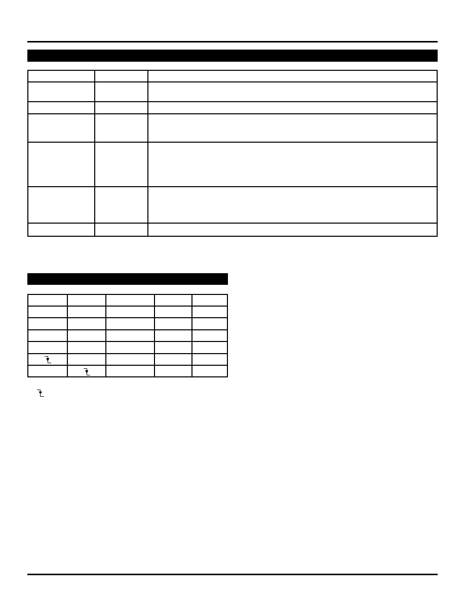
The SY89830U features a 2:1 input MUX, making it an
ideal solution for redundant clock switchover applications.
If only one input pair is used, the other pair may be left
floating. In addition, this device includes a synchronous
enable pin that forces the outputs into a fixed logic state.
Enable or disable state is initiated only after the outputs are
in a LOW state, thus eliminating the possibility of a "runt"
clock pulse.
The SY89830U I/O are fully differential and 100K ECL
compatible. Differential 10K ECL logic can interface directly
into the SY89830U inputs.
The SY89830U is part of Micrel's high-speed precision
edge timing and distribution family. For applications that
require a different I/O combination, consult the Micrel website
at www.micrel.com, and choose from a comprehensive
product line of high-speed, low-skew fanout buffers,
translators, and clock generators.
FEATURES
DESCRIPTION
Rev.: D
Amendment: /0
Issue Date:
November 2004
PIN CONFIGURATION/BLOCK DIAGRAM
s
Guaranteed AC parameters over temp/voltage:
∑ > 2.5GHz f
MAX
∑ < 25ps within-device skew
∑ < 225ps tr/tf time
∑ < 450ps prop delay
s
Low jitter design:
∑ < 1ps
(rms)
cycle-to-cycle jitter
∑ < 15ps
(pp)
total jitter
s
2:1 Differential MUX input
s
Flexible supply voltage: 2.5V/3.3V/5V
s
Wide operating temperature range: ≠40
∞
C to +85
∞
C
s
100K ECL compatible outputs
s
Inputs accept PECL/LVPECL/ECL/HSTL logic levels
s
Available in a 16-pin TSSOP package
1
Q0
/Q0
Q1
/Q1
Q2
/Q2
Q3
/Q3
16 VCC
/EN
/IN1
IN1
/IN0
IN0
IN_SEL
VEE
2
15
3
14
4
13
5
12
6
11
7
10
8
9
D
Q
1
0
Precision Edge is a trademark of Micrel, Inc.
Precision EdgeTM
Precision EdgeTM
SY89830U
2.5V/3.3/5V 2.5GHz 1:4 PECL/ECL
CLOCK DRIVER WITH 2:1
DIFFERENTIAL INPUT MUX
2
Precision EdgeTM
SY89830U
Micrel
M9999-111794
hbwhelp@micrel.com or (408) 955-1690
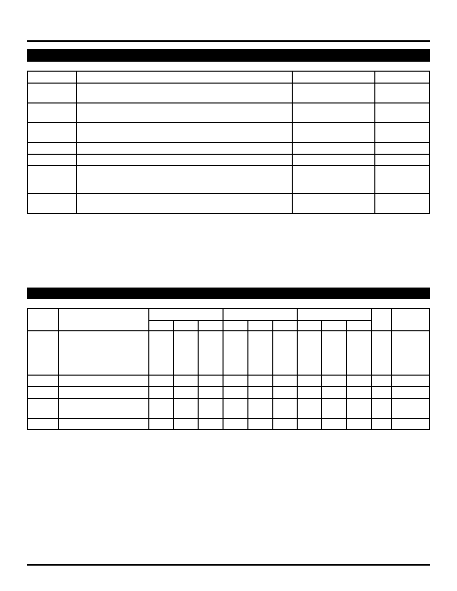
TRUTH TABLE
(1)
IN0
IN1
IN_SEL
/EN
Q
L
X
L
L
L
H
X
L
L
H
X
L
H
L
L
X
H
H
L
H
X
L
H
L
X
H
H
L
Note:
1. = negative edge
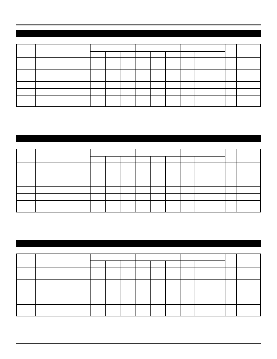
Pin Number
Pin Name
Pin Function
1, 2, 3, 4,
Q0 to Q3
(LV)PECL, (LV)ECL differential outputs: Terminate with 50
to V
CC
≠2V. For
5, 6, 7, 8
/Q0 to /Q3
single-ended applications, terminate the unused output with 50
to V
CC
≠2V.
9
V
EE
Negative Power Supply: For LVPECL, PECL applications, connect to GND.
10
IN_SEL
(LV)PECL, (LV)ECL compatible 2:1 mux input signal select: When IN_SEL is LOW, the
IN0 input pair is selected. When IN_SEL is HIGH, the IN1 input pair is selected. Includes a
75k
pull-down. Default state is LOW and IN0 is selected.
11, 12, 13, 14
IN0, /IN0
(LV)PECL, (LV)ECL, HSTL clock or data inputs.
IN1, /IN1
Internal 75k
pull-down resistors on IN0, IN1. Internal 75k
pull-up and 75k
pull-down
resistors on /IN0, /IN1.
/IN0, /IN1 default condition is V
CC
/2 when left floating. IN0, IN1 default condition is LOW
when left floating.
15
/EN
(LV)PECL, (LV)ECL compatible synchronous enable: When /EN goes HIGH, Q
OUT
will
go LOW and /Q
OUT
will go HIGH on the next LOW input clock transition. Includes a 75k
pull-down. Default state is LOW when left floating. The internal latch is clocked on the
falling edge of the input (IN0, IN1)
16
V
CC
Positive Power Supply: Bypass with 0.1
µ
F//0.01
µ
F low ESR capacitors.
PIN DESCRIPTION
3
Precision EdgeTM
SY89830U
Micrel
M9999-111794
hbwhelp@micrel.com or (408) 955-1690
Symbol
Rating
Value
Unit
V
CC
≠ V
EE
Power Supply Voltage
6.0
V
V
IN
Input Voltage (V
CC
= 0V, V
IN
not more negative than V
EE
)
≠6.0 to 0
V
Input Voltage (V
EE
= 0V, V
IN
not more positive than V
CC
)
+6.0 to 0
I
OUT
Output Current
≠Continuous
50
mA
≠Surge
100
T
A
Operating Temperature Range
≠40 to +85
∞
C
T
store
Storage Temperature Range
≠65 to +150
∞
C
JA
Package Thermal Resistance
≠Still-Air (single-layer PCB)
115
(Junction-to-Ambient)
≠Still-Air (multi-layer PCB)
75
∞
C/W
≠500lfpm (multi-layer PCB)
65
JC
Package Thermal Resistance
21
∞
C/W
(Junction-to-Case)
ABSOLUTE MAXIMUM RATINGS
(1)
Note:
1. Permanent device damage may occur if ABSOLUTE MAXIMUM RATINGS are exceeded. This is a stress rating only and functional operation is not implied
at conditions other than those detailed in the operational sections of this data sheet. Exposure to ABSOLUTE MAXIMUM RATlNG conditions for extended
periods may affect device reliability.
T
A
= ≠40
∞
C
T
A
= +25
∞
C
T
A
= +85
∞
C
Symbol
Parameter
Min.
Typ.
Max.
Min.
Typ.
Max.
Min.
Typ.
Max.
Unit
Condition
V
CC
Power Supply Voltage
V
(PECL)
4.5
5.0
5.5
4.5
5.0
5.5
4.5
5.0
5.5
(LVPECL)
2.375
3.3
3.63
2.375
3.3
3.63
2.375
3.3
3.63
(ECL)
≠5.5
≠5.0
≠4.5
≠5.5
≠5.0
≠4.5
≠5.5
≠5.0
≠4.5
(LVECL)
≠3.63
≠3.3
≠2.375 ≠3.63
≠3.3
≠2.375 ≠3.63
≠3.3
≠2.375
I
CC
Power Supply Current
--
--
70
--
50
72
--
--
75
mA
I
IH
Input HIGH Current
--
--
150
--
--
150
--
--
150
µ
A
V
IN
= V
IH
I
IL
Input LOW Current
IN
0.5
--
--
0.5
--
--
0.5
--
--
µ
A
V
IN
= V
IL
/IN
≠150
--
--
≠150
--
--
≠150
--
--
µ
A
V
IN
= V
IL
C
IN
Input Capacitance (TSSOP)
--
--
--
--
1.0
--
--
--
--
pF
DC ELECTRICAL CHARACTERISTICS
(1)
Note:
1. 100KEP circuits are designed to meet the DC specifications shown in the above table after thermal equilibrium has been established. The circuit is in a
test socket or mounted on a printed circuit board and traverse airflow greater than 500lfpm is maintained.
4
Precision EdgeTM
SY89830U
Micrel
M9999-111794
hbwhelp@micrel.com or (408) 955-1690
T
A
= ≠40
∞
C
T
A
= +25
∞
C
T
A
= +85
∞
C
Symbol
Parameter
Min.
Typ.
Max.
Min.
Typ.
Max.
Min.
Typ.
Max.
Unit
Condition
V
IL
Input LOW Voltage
555
--
875
555
--
875
555
--
875
mV
V
CC
= 2.5V
(Single-ended)
V
IH
Input HIGH Voltage
1275
--
1620
1275
--
1620
1275
--
1620
mV
V
CC
= 2.5V
(Single-ended)
V
OL
Output LOW Voltage
555
680
805
555
680
805
555
680
805
mV
V
CC
= 2.5V
V
OH
Output HIGH Voltage
1355
1480
1605
1355
1480
1605
1355
1480
1605
mV
V
CC
= 2.5V
V
IHCMR
Input HIGH Voltage
1.2
--
V
CC
1.2
--
V
CC
1.2
--
V
CC
V
Common Mode Range
(2)
(100KEP) LVPECL DC ELECTRICAL CHARACTERISTICS
(1)
V
CC
= 2.5V
±
5%, V
EE
= 0V
Notes:
1. 100KEP circuits are designed to meet the DC specifications shown in the above table after thermal equilibrium has been established. The circuit is in a
test socket or mounted on a printed circuit board and traverse airflow greater than 500lfpm is maintained. Input and output parameters vary 1:1 with V
CC
.
Output load is 50
to V
CC
≠2V.
2. The V
IHCMR
range is referenced to the most positive side of the differential input signal.
T
A
= ≠40
∞
C
T
A
= +25
∞
C
T
A
= +85
∞
C
Symbol
Parameter
Min.
Typ.
Max.
Min.
Typ.
Max.
Min.
Typ.
Max.
Unit
Condition
V
IL
Input LOW Voltage
1355
--
1675
1355
--
1675
1355
--
1675
mV
V
CC
= 3.3V
(Single-Ended)
V
IH
Input HIGH Voltage
2075
--
2420
2075
--
2420
2075
--
2420
mV
V
CC
= 3.3V
(Single-Ended)
V
OL
Output LOW Voltage
1355
1480
1605
1355
1480
1605
1355
1480
1605
mV
V
CC
= 3.3V
V
OH
Output HIGH Voltage
2155
2280
2405
2155
2280
2405
2155
2280
2405
mV
V
CC
= 3.3V
V
IHCMR
Input HIGH Voltage
1.2
--
V
CC
1.2
--
V
CC
1.2
--
V
CC
V
Common Mode Range
(2)
(100KEP) LVPECL DC ELECTRICAL CHARACTERISTICS
(1)
V
CC
= 3.3V
±
10%, V
EE
= 0V
Notes:
1. 100KEP circuits are designed to meet the DC specifications shown in the above table after thermal equilibrium has been established. The circuit is in a
test socket or mounted on a printed circuit board and traverse airflow greater than 500lfpm is maintained. Input and output parameters vary 1:1 with V
CC
.
Output load is 50
to V
CC
≠2V.
2. The V
IHCMR
range is referenced to the most positive side of the differential input signal.
T
A
= ≠40
∞
C
T
A
= +25
∞
C
T
A
= +85
∞
C
Symbol
Parameter
Min.
Typ.
Max.
Min.
Typ.
Max.
Min.
Typ.
Max.
Unit
Condition
V
IL
Input LOW Voltage
3055
--
3375
3055
--
3375
3055
--
3375
mV
V
CC
= 5.0V
(Single-Ended)
V
IH
Input HIGH Voltage
3775
--
4120
3775
--
4120
3775
--
4120
mV
V
CC
= 5.0V
(Single-Ended)
V
OL
Output LOW Voltage
3055
3180
3305
3055
3180
3305
3055
3180
3305
mV
V
CC
= 5.0V
V
OH
Output HIGH Voltage
3855
3980
4105
3855
3980
4105
3855
3980
4105
mV
V
CC
= 5.0V
V
IHCMR
Input HIGH Voltage
(2)
1.2
--
V
CC
1.2
--
V
CC
1.2
--
V
CC
V
Common Mode Range
(100KEP) PECL DC ELECTRICAL CHARACTERISTICS
(1)
V
CC
= 5.0V
±
10%, V
EE
= 0V
Notes:
1. 100KEP circuits are designed to meet the DC specifications shown in the above table after thermal equilibrium has been established. The circuit is in a
test socket or mounted on a printed circuit board and traverse airflow greater than 500lfpm is maintained. Input and output parameters vary 1:1 with V
CC
.
Output load is 50
to V
CC
≠2V.
2. The V
IHCMR
range is referenced to the most positive side of the differential input signal.
5
Precision EdgeTM
SY89830U
Micrel
M9999-111794
hbwhelp@micrel.com or (408) 955-1690
T
A
= ≠40
∞
C
T
A
= +25
∞
C
T
A
= +85
∞
C
Symbol
Parameter
Min.
Typ.
Max.
Min.
Typ.
Max.
Min.
Typ.
Max.
Unit
Condition
V
IL
Input LOW Voltage
≠1945
--
≠1625 ≠1945
--
≠1625 ≠1945
--
≠1625
mV
(Single-ended)
V
IH
Input HIGH Voltage
≠1225
--
≠880
≠1225
--
≠880
≠1225
--
≠880
mV
(Single-ended)
V
OL
Output LOW Voltage
≠1945 ≠1820 ≠1695 ≠1945 ≠1820 ≠1695 ≠1945 ≠1820 ≠1695
mV
50
to V
CC
≠2V
V
OH
Output HIGH Voltage
≠1145 ≠1020
≠895
≠1145 ≠1020
≠895
≠1145 ≠1020
≠895
mV
50
to V
CC
≠2V
V
IHCMR
Input HIGH Voltage
V
EE
+1.2
--
0.0
V
EE
+1.2
--
0.0
V
EE
+1.2
--
0.0
V
Common Mode Range
(2)
(100KEP) LVECL DC ELECTRICAL CHARACTERISTICS
(1)
V
CC
= 0V, V
EE
= ≠2.375V to ≠3.63V
Notes:
1. 100KEP circuits are designed to meet the DC specifications shown in the above table after thermal equilibrium has been established. The circuit is in a
test socket or mounted on a printed circuit board and traverse airflow greater than 500lfpm is maintained.
2. The V
IHCMR
range is referenced to the most positive side of the differential input signal.
(100KEP) ECL DC ELECTRICAL CHARACTERISTICS
(1)
V
CC
= 0V, V
EE
= ≠4.5V to ≠5.5V
Notes:
1. 100KEP circuits are designed to meet the DC specifications shown in the above table after thermal equilibrium has been established. The circuit is in a
test socket or mounted on a printed circuit board and traverse airflow greater than 500lfpm is maintained.
2. The V
IHCMR
range is referenced to the most positive side of the differential input signal.
T
A
= ≠40
∞
C
T
A
= +25
∞
C
T
A
= +85
∞
C
Symbol
Parameter
Min.
Typ.
Max.
Min.
Typ.
Max.
Min.
Typ.
Max.
Unit
Condition
V
IL
Input LOW Voltage
≠1945
--
≠1625 ≠1945
--
≠1625 ≠1945
--
≠1625
mV
(Single-ended)
V
IH
Input HIGH Voltage
≠1225
--
≠880
≠1225
--
≠880
≠1225
--
≠880
mV
(Single-ended)
V
OL
Output LOW Voltage
≠1945 ≠1820 ≠1695 ≠1945 ≠1820 ≠1695 ≠1945 ≠1820 ≠1695
mV
50
to V
CC
≠2V
V
OH
Output HIGH Voltage
≠1145 ≠1020
≠895
≠1145 ≠1020
≠895
≠1145 ≠1020
≠895
mV
50
to V
CC
≠2V
V
IHCMR
Input HIGH Voltage
V
EE
+1.2
--
0.0
V
EE
+1.2
--
0.0
V
EE
+1.2
--
0.0
V
Common Mode Range
(2)
T
A
= ≠40
∞
C
T
A
= +25
∞
C
T
A
= +85
∞
C
Symbol
Parameter
Min.
Typ.
Max.
Min.
Typ.
Max.
Min.
Typ.
Max.
Unit
V
IH
Input HIGH Voltage
1200
--
--
1200
--
--
1200
--
--
mV
V
IL
Input LOW Voltage
--
--
400
--
--
400
--
--
400
mV
HSTL INPUT DC ELECTRICAL CHARACTERISTICS
V
CC
= 2.375V to 3.63V, V
EE
= 0V