DESCRIPTION
I Guaranteed AC performance over temperature
and voltage
∑ > 2.0GHz f
MAX
∑ < 20ps within-device skew
∑ < 225ps rise/fall times
I Low jitter design
∑ < 1ps(rms) cycle-to-cycle
∑ < 10ps(pk-pk) total jitter
I Unique input termination and V
T
pin for DC-coupled
and AC-coupled inputs (CML, HSTL, and LVPECL)
I Fully differential I/O design
I Low power 2.5V and 3.3V power supply
I TTL/CMOS compatible enable input
I Wide operating temperature range: ≠40
∞
C to +85
∞
C
I Available in 16-pin (3mm ◊ 3mm) MLFTM package
FEATURES
2GHz ANY DIFF. IN-TO-LVPECL ULTRA
LOW-JITTER AND SKEW 1:4 FANOUT
BUFFER/TRANSLATOR W/ INTERNAL TERMINATION
Precision EdgeTM
SY89831U
FINAL
APPLICATIONS
I Processor clock distribution
I SONET clock distribution
I Fibre Channel clock distribution
I Gigabit Ethernet clock distribution
1
Rev.: C
Amendment: /0
Issue Date:
February 2003
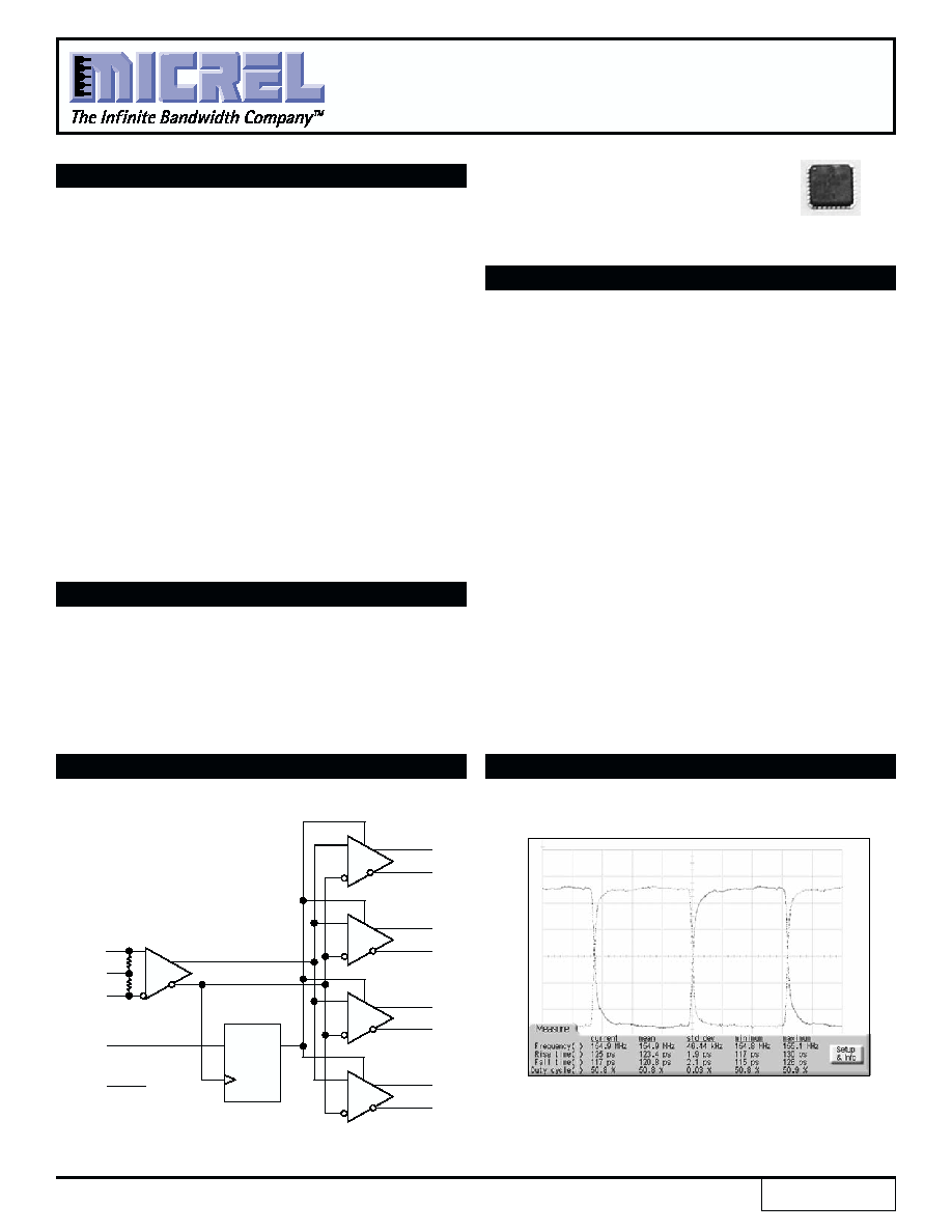
The SY89831U is a high-speed, 2GHz differential
LVPECL 1:4 fanout buffer optimized for ultra-low skew
applications. Within device skew is guaranteed to be less
than 20ps (5ps typ.) over supply voltage and temperature.
The differential input buffer has a unique internal termination
design that allows access to the termination network through
a V
T
pin. This feature allows the device to easily interface
to different logic standards. A V
REF≠AC
reference output is
included for AC-coupled applications.
The SY89831U is a part of Micrel's high-speed clock
synchronization family. For applications that require a
different I/O combination, consult Micrel's website at
www.micrel.com, and choose from a comprehensive product
line of high-speed, low-skew fanout buffers, translators and
clock generators.
FUNCTIONAL BLOCK DIAGRAM
TYPICAL PERFORMANCE
Precision Edge is a trademark of Micrel, Inc.
MicroLeadFrame and MLF are trademarks of Amkor Technology, Inc.
IN
/IN
D
Q
Q3
/Q3
Q2
/Q2
Q1
/Q1
Q0
/Q0
EN
V
T
50
50
V
REF--AC
155MHz Output
TIME (1ns/div.)
Output Swing
(150mV/div
.)
T
A
= 25
∞C
V
CC
= 3.3V
V
EE
GND
V
IN
= 800mV
/Q
Q
Precision EdgeTM
2
Precision EdgeTM
SY89831U
Micrel
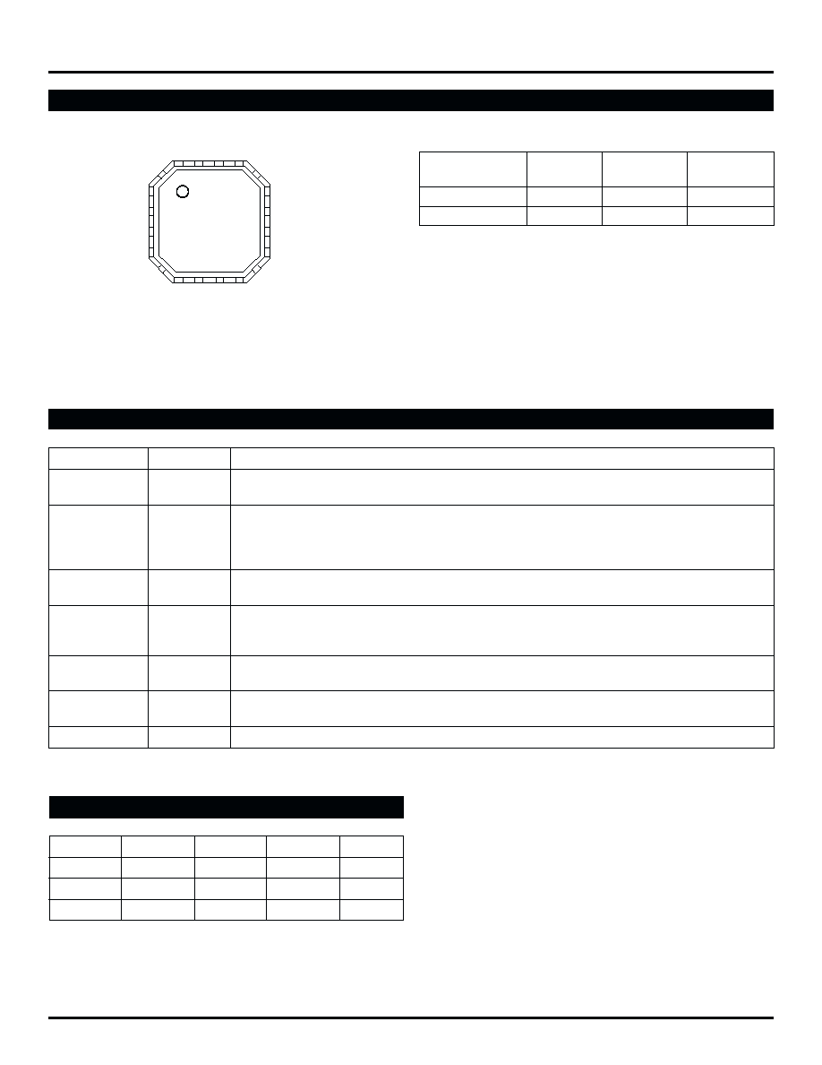
PACKAGE/ORDERING INFORMATION
Ordering Information
Package
Operating
Package
Part Number
Type
Range
Marking
SY89831UMI
MLF-16
Industrial
831U
SY89831UMITR*
MLF-16
Industrial
831U
*Tape and Reel
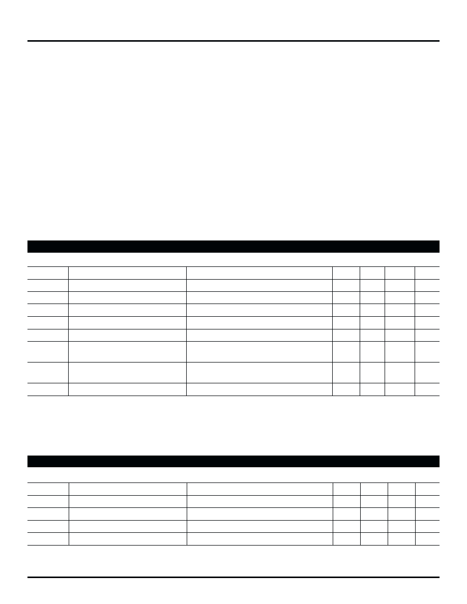
Pin Number
Pin Name
Pin Function
15, 16
(Q0, /Q0) to
LVPECL Differential (Outputs): Terminate to V
CC
≠2V. See
"Termination Recommendations"
1, 2, 3, 4, 5, 6
(Q3, /Q3)
section. Unused output pairs may be left floating with no impact on jitter.
8
EN
TTL/CMOS Compatible Synchronous Enable: When EN goes LOW, Q outputs will go LOW
and /Q outputs will go HIGH on the next LOW transition at D inputs. Input threshold is V
CC
/2V.
Includes a 25k
pull-up resistor. Default state is HIGH when left floating. The internal latch is
clocked on the falling edge of the input signal (IN, /IN).
9, 12
/IN, IN
Differential Clock (Inputs): Internal 50
termination resistors to V
T
pin. See
"Input Interface
Applications" section.
10
VREF≠AC
Reference Voltage: Equal to V
CC
≠1.4V (approx.), and used for AC≠coupled applications.
Maximum sink/source current is 0.5mA. See
"Input Interface Applications" section. When using
V
REF≠AC
, bypass with a 0.01
µF capacitor to V
CC
.
11
VT
Termination Center-Tap: For CML inputs, leave this pin floating. Otherwise, see Figures 2a to 2e
in
"Input Interface Applications" section.
13,
GND
Ground. Exposed pad is internally connected to GND and must be connected to a ground plane
Exposed Pad
for proper thermal operation.
14
VCC
Positive Power Supply: Bypass with 0.1
µF//0.01µF low ESR capacitors.
PIN DESCRIPTION
1
2
3
4
12
11
10
9
16 15 14 13
5
6
7
8
Q1
/Q1
Q2
/Q2
IN
VT
VREF≠AC
/IN
GND
VCC
Q0
/Q0
EN
VCC
/Q3
Q3
16-Pin MLFTM
IN
/IN
EN
Q
/Q
0
1
1
0
1
1
0
1
1
0
X
X
0
0
(1)
1
(1)
Note 1.
On next negative transition of the input signal (IN).
TRUTH TABLE
3
Precision EdgeTM
SY89831U
Micrel
Absolute Maximum Ratings
(Note 1)
Supply Voltage (V
CC
) .................................. ≠0.5V to +4.0V
Input Voltage (V
IN
) ............................... ≠0.5V to V
CC
+0.5V
Output Current (I
OUT
)
Continuous ......................................................... 50mA
Surge ................................................................ 100mA
Input Current (IN, /IN) ...............................................
±50mA
V
T
Current (I
VT
) .......................................................
±100µA
Input Sink/Source Current (V
REF≠AC
), Note 3 .........
±0.5mA
Lead Temperature (soldering, 10sec.) ...................... 220
∞C
Storage Temperature (T
S
) ....................... ≠65
∞C to +150∞C
Operating Ratings
(Note 2)
Supply Voltage Range .......................... +2.375V to +3.63V
Ambient Temperature (T
A
) ......................... ≠40
∞C to +85∞C
Package Thermal Resistance
MLFTM
(
JA
)
Still-Air ............................................................. 60
∞C/W
500lfpm ............................................................ 54
∞C/W
MLFTM
(
JB
), Note 4
Junction-to-Board ............................................ 32
∞C/W
T
A
= ≠40
∞C to +85∞C
Symbol
Parameter
Condition
Min
Typ
Max
Units
V
CC
Power Supply Voltage Range
2.375
3.63
V
I
CC
Power Supply Current
No load, maximum supply voltage
47
70
mA
R
IN
Differential Input Resistance (IN, /IN)
80
100
120
V
IH
Input HIGH Voltage (IN, /IN)
Note 3
1.2
V
CC
V
V
IL
Input LOW Voltage (IN, /IN)
Note 3
0
V
CC
≠0.1
V
V
IN
Input Voltage Swing
Note 3, see Figure 1a, and 1b.
0.1
2.8
V
V
T
floating for V
IN
(max.)
V
DIFF_IN
Differential Input Voltage Swing,
see Figure 1a, and 1b.
0.2
V
Note 3
|I
IN
|
Input Current (IN, /IN)
Note 3
35
mA
Note 1.
The circuit is designed to meet the DC specifications shown in the above table after thermal equilibrium has been established.
Note 2.
Specification for packaged product ony.
Note 3.
Due to the internal termination (see
"Differential Input" ) the input current depends on the applied voltages at IN, /IN and V
T
inputs. Do not apply
a combination of voltages that causes the input current to exceed the maximum limit.
DC ELECTRICAL CHARACTERISTICS
(Note 1, 2)
V
CC
= 2.375V to 3.63V; V
EE
= 0V; T
A
= ≠40
∞C to +85∞C
Symbol
Parameter
Condition
Min
Typ
Max
Units
V
IH
Input HIGH Voltage
2.0
V
CC
V
V
IL
Input LOW Voltage
0
0.8
V
I
IH
Input HIGH Current
20
≠125
µA
I
IL
Input LOW Current
≠300
µA
Note 1.
Specification for packaged product ony.
LVTTL/LVCMOS INPUT DC ELECTRICAL CHARACTERISTICS
(Note 1)
Note 1.
Permanent device damage may occur if ABSOLUTE MAXIMUM RATINGS are exceeded. This is a stress rating only and functional operation is
not implied at conditions other than those detailed in the operational sections of this data sheet. Exposure to ABSOLUTE MAXIMUM RATlNG
conditions for extended periods may affect device reliability.
Note 2.
The data sheet limits are not guaranteed if the device is operated beyond the operating ratings.
Note 3.
Due to the limited drive capability use for input of the same package only.
Note 4.
Junction-to-board resistance assumes exposed pad is soldered (or equivalent) to the device's most negative potential on the PCB.
4
Precision EdgeTM
SY89831U
Micrel
V
CC
= 2.5V
±5%; V
EE
= 0V; T
A
= ≠40
∞C to +85∞C
Symbol
Parameter
Condition
Min
Typ
Max
Units
V
OH
Output HIGH Voltage
R
L
=
50
to V
CC
≠2V
1355
1480
1605
mV
V
OL
Output LOW Voltage
R
L
=
50
to V
CC
≠2V
555
680
805
mV
V
OUT
Output Voltage Swing
see Figure 1a, and 1b
550
800
1050
mV
V
DIFF_OUT
Differential Output Voltage Swing
see Figure 1a, and 1b
1100
1600
2100
mV
Note 1.
The circuit is designed to meet the DC specifications shown in the above table after thermal equilibrium has been established. The circuit is in a
test socket or mounted on a printed circuit board and traverse airflow greater than 500lfpm is maintained. Parameters are for V
CC
= 2.5V. They
vary 1:1 with V
CC
.
Note 2.
Specification for packaged product only.
2.5V (100KEP) LVPECL DC ELECTRICAL CHARACTERISTICS
(Note 1, 2)
V
CC
= 3.3V
±10%; V
EE
= 0V; T
A
= ≠40
∞C to +85∞C
Symbol
Parameter
Condition
Min
Typ
Max
Units
V
OH
Output HIGH Voltage
R
L
=
50
to V
CC
≠2V
2155
2280
2405
mV
V
OL
Output LOW Voltage
R
L
=
50
to V
CC
≠2V
1355
1480
1605
mV
V
REF≠AC
Reference Voltage, Note 2
1755
1875
1975
mV
Note 1.
The circuit is designed to meet the DC specifications shown in the above table after thermal equilibrium has been established.
Note 2.
Specification for packaged product only.
Note 3.
Single-ended input operation is limited to V
CC
3.0V.
3.3V (100KEP) LVPECL DC ELECTRICAL CHARACTERISTICS
(Note 1, 2)
5
Precision EdgeTM
SY89831U
Micrel
V
CC
= 2.375 to 3.63V; V
EE
= 0V; T
A
= ≠40
∞C to +85∞C, output loading is 50 to V
CC
≠2V, unless otherwise noted.
Symbol
Parameter
Condition
Min
Typ
Max
Units
f
MAX
Maximum Frequency
Output Swing
450mV
2.0
2.5
GHz
t
PLH
Propagation Delay-to-Output
Input Swing: 100mV
390
0
ps
t
PHL
(Differential)
Input Swing: 800mV
250
350
450
ps
t
SKEW
Within-Device Skew (Differential)
Note 3
5
20
ps
Part-to-Part Skew (Differential)
150
ps
t
S
Set-Up Time (EN to IN, /IN)
Note 4
300
ps
t
H
Hold Time (EN to IN, /IN)
Note 4
300
ps
t
JITTER
Cycle-to-Cycle Jitter (rms)
Note 5
1
ps(rms)
Total Jitter
Note 6
10
ps(pk-pk)
t
r
,
t
f
Output Rise/Fall Times
70
150
225
ps
(20% to 80%)
Note 1.
Measured with 400mV input signal, 50% duty cycle, all loading with 50
to V
CC
≠2V. Output swing is
450mV.
Note 2.
Specification for packaged product only.
Note 3.
Skew is measured between outputs under identical transitions.
Note 4.
Set-up and hold times apply to synchronous applications that intend to enable/disable before the next clock cycle. For asynchronous applica-
tions, set-up and hold times do not apply.
Note 5.
Cycle-to-cycle jitter definition: The variation period between adjacent cycles over a random sample of adjacent cycle pairs.
T
JITTER_CC
= T
n
≠T
n+1
, where T is the time between rising edges of the output signal.
Note 6.
Total jitter definition: with an ideal clock input frequency of
f
MAX
(device), no more than one output edge in 10
12
output edges will deviate by
more than the specified peak-to-peak jitter value.
AC ELECTRICAL CHARACTERISTICS
(Note 1, 2)
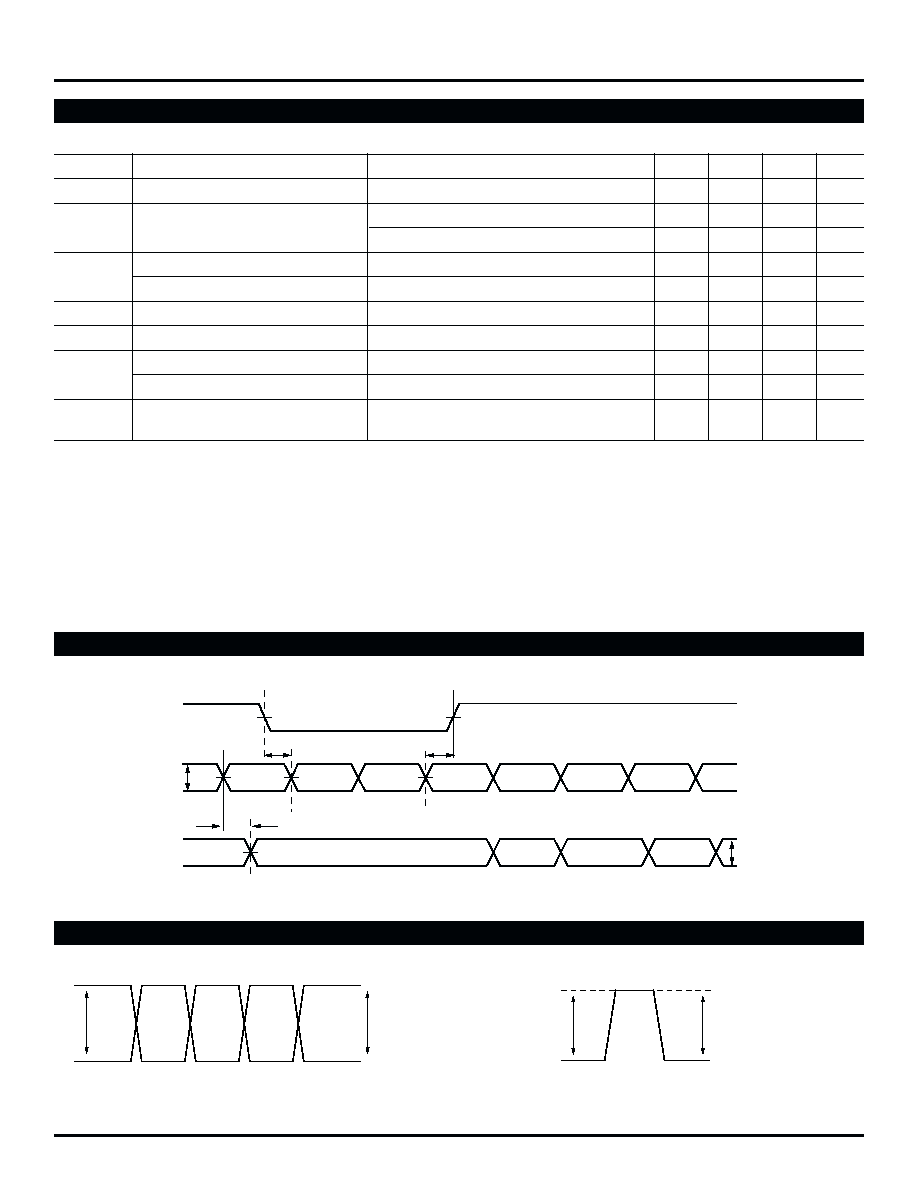
TIMING DIAGRAM
t
S
IN
/Q
Q
t
PLH
,
t
PLH
t
H
EN
V
CC
/2
V
OUT
Swing
V
CC
/2
V
IN
/IN
V
IN,
V
OUT
Q
OUT
/Q
OUT
800mV (typical)
Figure 1a. Single-Ended Swing
1.6V (typical)
V
DIFF_IN
,
V
DIFF_OUT
Q
OUT
/Q
OUT
Figure 1b. Differential Swing
DEFINITION OF SINGLE-ENDED AND DIFFERENTIAL SWING