
SY89840U
Precision LVPECL Runt Pulse Eliminator 2:1
Multiplexer
Precision Edge is a registered trademark of Micrel, Inc.
MLF and MicroLeadFrame are trademarks of Amkor Technology, Inc.
Micrel Inc. ∑ 2180 Fortune Drive ∑ San Jose, CA 95131 ∑ USA ∑ tel +1 (408) 944-0800 ∑ fax + 1 (408) 474-1000 ∑ http://www.micrel.com
February 2005
M9999-021705
hbwhelp@micrel.com
or (408) 955-1690
General Description
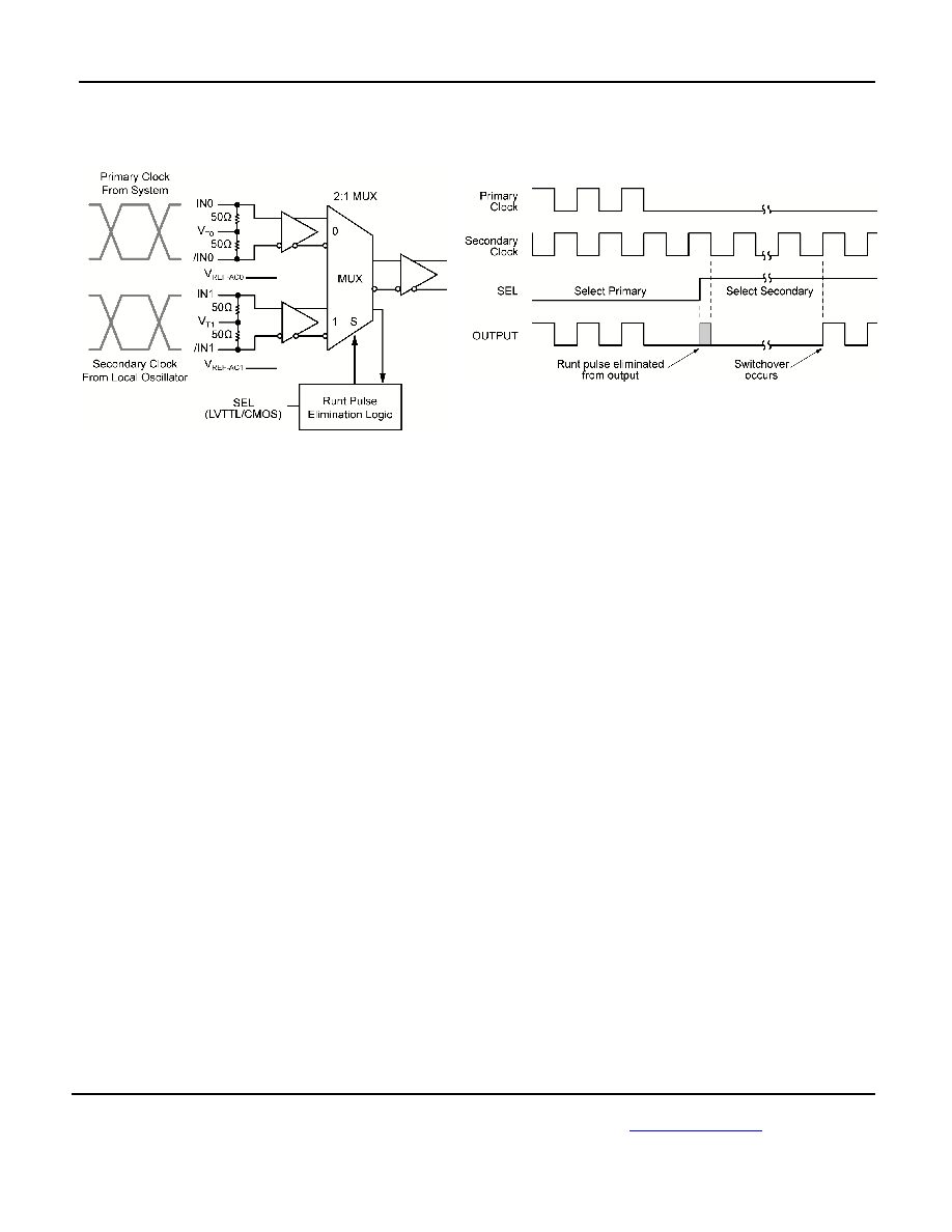
The SY89840U is a low jitter PECL, 2:1 differential input
multiplexer (MUX) optimized for redundant source
switchover applications. Unlike standard multiplexers,
the SY89840U unique 2:1 Runt Pulse Eliminator (RPE)
MUX prevents any short cycles or "runt" pulses during
switchover. In addition, a unique Fail-Safe Input
protection prevents metastable conditions when the
selected input clock fails to a DC voltage (voltage
between the pins of the differential input drops below
100mV).
The differential input includes Micrel's unique, 3-pin
input termination architecture that allows customers to
interface to any differential signal (AC or DC-coupled) as
small as 100mV (200mV
pp
) without any level shifting or
termination resistor networks in the signal path. The
output is 800mV, 100K compatible LVPECL with fast
rise/fall times guaranteed to be less than 190ps.
The SY89840U operates from a 2.5V ±5% or 3.3V
±10% supply and is guaranteed over the full industrial
temperature range of ≠40∞C to +85∞C. The SY89840U is
part of Micrel's high-speed, Precision Edge
Æ
product
line. All support documentation can be found on Micrel's
web site at:
www.micrel.com
.
Precision Edge
Æ
Features
∑ Selects between two sources, and provides a glitch-free,
stable LVPECL output
∑ Guaranteed AC performance over temperature and supply
voltage:
≠ Wide operating frequency: 1kHz to >1.5GHz
≠ < 880ps In-to-Out t
pd
≠ < 190ps t
r
/t
f
∑ Unique patent-pending input isolation design minimizes
crosstalk
∑ Fail-safe input prevents oscillations
∑ Ultra-low jitter design:
≠ <1ps
rms
random jitter
≠ <1ps
rms
cycle-to-cycle jitter
≠ <10ps
pp
total jitter (clock)
≠ <0.7ps
rms
MUX crosstalk induced jitter
∑ Unique patent-pending input termination and VT pin
accepts DC-coupled and AC-coupled inputs (CML,
PECL, LVDS)
∑ 800mV LVPECL output swing
∑ 2.5V ±5% or 3.3V ±10% supply voltage
∑ ≠40∞C to +85∞C industrial temperature range
∑ Available in 16-pin (3mm x 3mm) MLF
TM
package
Applications
∑ Redundant clock switchover
∑ Failsafe clock protection
Markets
∑ LAN/WAN
∑ Enterprise
servers
∑ ATE
∑ Test and measurement
Micrel, Inc.
SY89840U
February 2005
2
M9999-021705
hbwhelp@micrel.com
or (408) 955-1690
Typical Application
Simplified Example Illustrating RPE (Runt Pulse Elimination)
Circuit when Primary Clock Fails
Micrel, Inc.
SY89840U
February 2005
3
M9999-021705
hbwhelp@micrel.com
or (408) 955-1690
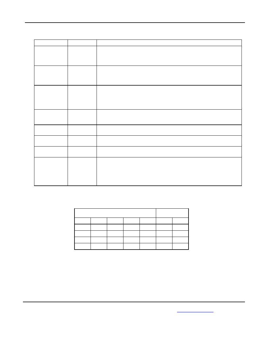
Ordering Information
(1)
Part Number
Package Type
Operating Range
Package Marking
Lead Finish
SY89840UMG
MLF-16
Industrial
840U with bar-line
Pb-Free indicator
NiPdAu
Pb-Free
SY89840UMGTR
(2)
MLF-16
Industrial
840U with bar-line
Pb-Free indicator
NiPdAu
Pb-Free
Notes:
1. Contact factory for die availability. Dice are guaranteed at T
A
= 25∞C, DC Electricals Only.
2. Tape and Reel.
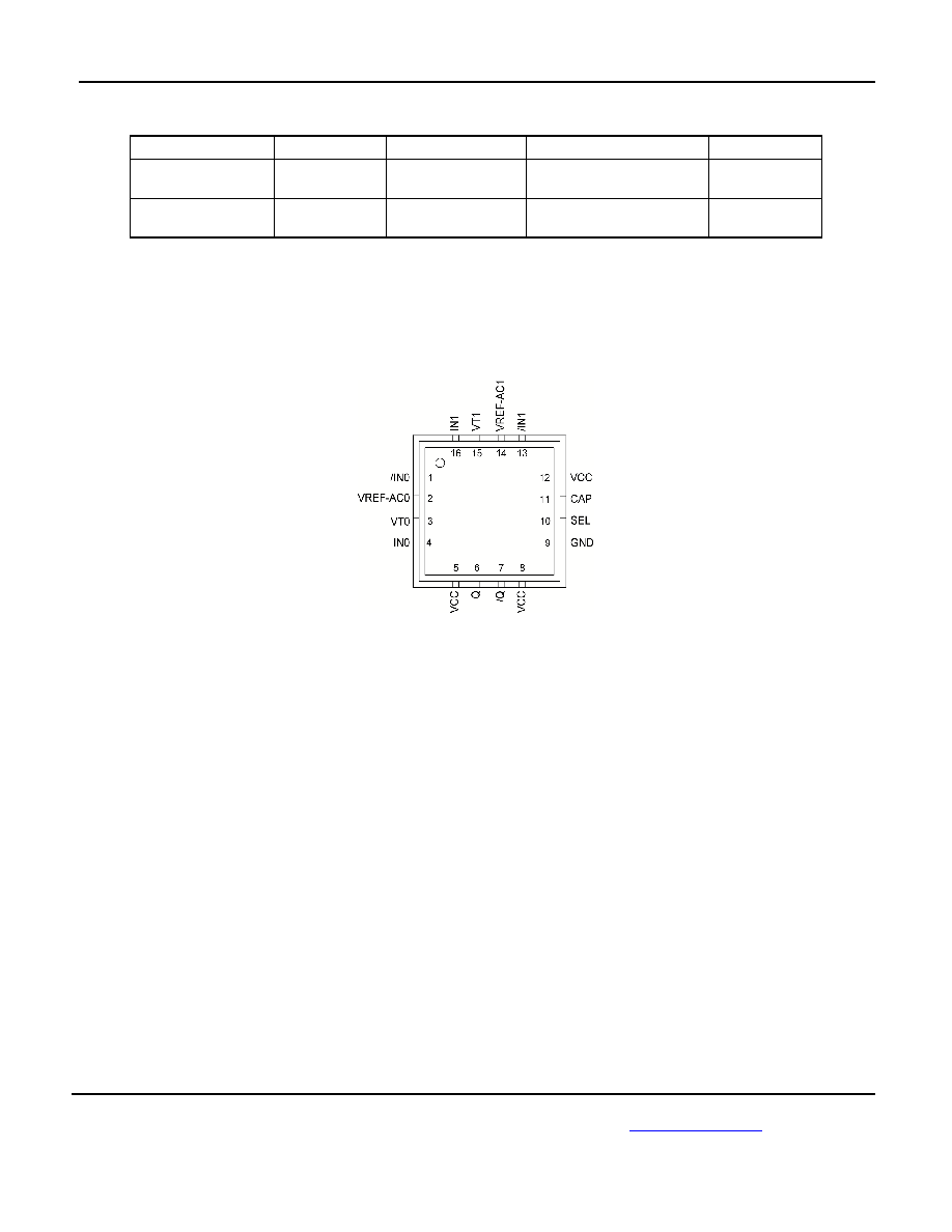
Pin Configuration
16-Pin MLF
TM
(MLF-16)
Micrel, Inc.
SY89840U
February 2005
4
M9999-021705
hbwhelp@micrel.com
or (408) 955-1690
Pin Description
Pin Number
Pin Name
Pin Function
4, 1,
16, 13
IN0, /IN0,
IN1, /IN1
Differential Inputs: These input pairs are the differential signal inputs to the
device. These inputs accept AC or DC-coupled signals as small as 100mV
(200mV
pp
). Each pin of a pair internally terminates to a VT
pin through 50 .
Please refer to the "Input Interface Applications" section for more details.
3, 15
VT0, VT1
Input Termination Center-Tap: Each side of the differential input pair terminates
to a VT pin. The VT0 and VT1 pins provide a center-tap to a termination network
for maximum interface flexibility. See the "Input Interface Applications" section for
more details.
2, 14
VREF-AC0
VREF-AC1
Reference Voltage: This output biases to V
CC
≠1.2V. It is used for AC-coupling
inputs IN and /IN. Connect VREF-AC directly to the corresponding VT pin. Bypass
with 0.01 F low ESR capacitor to V
CC
. Maximum sink/source current is ±1.5mA.
Due to the limited drive capability, the VREF-AC pin is only intended to drive its
respective VT pin. See "Input Interface Applications" section.
10
SEL
This single-ended TTL/CMOS-compatible input selects the inputs to the
multiplexer. Note that this input is internally connected to a 25k pull-up resistor
and will default to a logic HIGH state if left open.
5, 8, 12
VCC
Positive Power Supply: Bypass with 0.1 F//0.01 F low ESR capacitors as close
to VCC pins as possible.
6, 7
Q, /Q
Differential Outputs: This differential LVPECL output is a logic function of the IN0,
IN1, and SEL inputs. Please refer to the truth table below for details.
9
GND
Exposed Pad
Ground: Ground pin and exposed pad must be connected to the same ground
plane.
11
CAP
Power-On Reset (POR) Initialization capacitor. When using the multiplexer with
RPE capability, this pin is tied to a capacitor to V
CC
. The purpose is to ensure the
internal RPE logic starts up in a known state. See "Power-On Reset (POR)
Description" section for more details regarding capacitor selection. If this pin is
tied directly to V
CC
, the RPE function will be disabled and the multiplexer will
function as a normal multiplexer. The CAP pin should never be left open.
Truth Table
INPUTS
OUTPUTS
IN0
/IN0
IN1
/IN1
SEL
Q
/Q
0
1
X
X
0
0
1
1
0
X
X
0
1
0
X
X
0
1
1
0
1
X
X
1
0
1
1
0
Micrel, Inc.
SY89840U
February 2005
5
M9999-021705
hbwhelp@micrel.com
or (408) 955-1690
Absolute Maximum Ratings
(1)
Supply Voltage (V
CC
) .................................................≠0.5V to +4.0V
Input Voltage (V
IN
) .........................................................≠0.5V to V
CC
LVPECL Output Current (I
OUT
)
Continuous ............................................................ ±50mA
Surge ................................................................... ±100mA
Termination Current
Source/Sink Current on V
T
............................................±100mA
Source/Sink Current on IN, /IN .......................................±50mA
V
REF-AC
Current
Source/sink current on V
REF-AC
.........................................±2mA
Lead Temperature (soldering, 20 sec.).................................+260∞C
Storage Temperature (Ts) .......................................≠65∞C to 150
∞C
Operating Ratings
(2)
Supply Voltage (V
CC
)............................... +2.375V to +2.625V
.................................................................. +3.0V to +3.6V
Ambient Temperature (T
A
) ............................. ≠40∞C to +85∞C
Package Thermal Resistance
(3)
MLFTM (
JA
)
Still-Air .................................................................. 60∞C/W
MLFTM (
JB
)
Junction-to-Board................................................. 33∞C/W
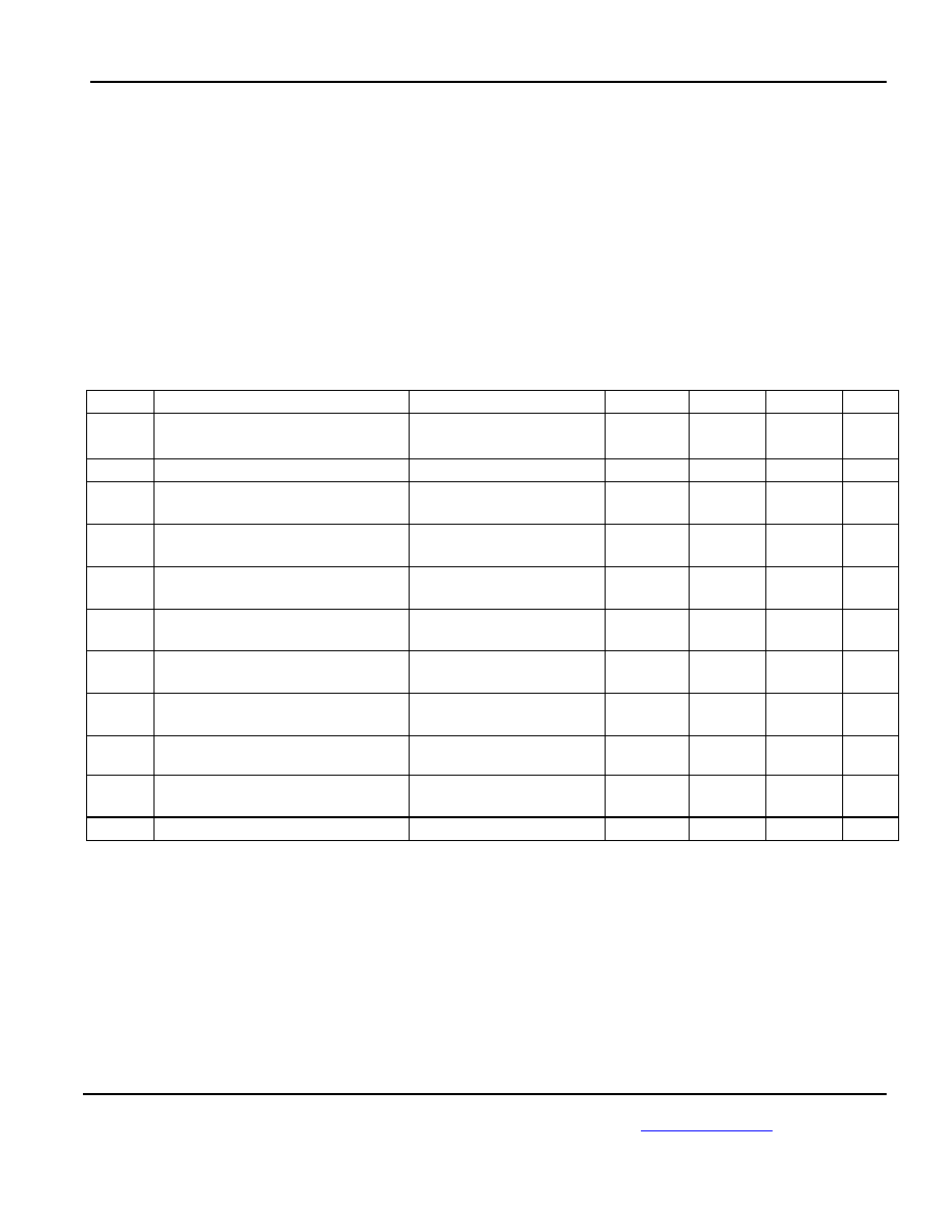
DC Electrical Characteristics
(4)
T
A
= ≠40∞C to +85∞C; unless otherwise stated.
Symbol
Parameter
Condition
Min
Typ
Max
Units
V
CC
Power Supply
2.375
3.0
2.625
3.6
V
V
I
CC
Power Supply Current
No load, max V
CC
.
65
95
mA
R
IN
Input Resistance
(IN-to-V
T
)
45
50
55
R
DIFF_IN
Differential Input Resistance
(IN-to-/IN)
90
100
110
V
IH
Input High Voltage
(IN, /IN)
1.2
V
CC
V
V
IL
Input Low Voltage
(IN, /IN)
0
V
IH
≠0.1
V
V
IN
Input Voltage Swing
(IN, /IN)
See Figure 1a. Note 5
0.1
V
CC
V
V
DIFF_IN
Differential Input Voltage Swing
|IN-/IN|
See Figure 1b.
0.2
V
V
IN_FSI
Input Voltage Threshold that Triggers
FSI
30
100
mV
V
T_IN
IN-to-V
T
(IN, /IN)
1.28
V
V
REF-AC
Output Reference Voltage
V
CC
≠1.3
V
CC
≠1.2
V
CC
≠1.1
V
Notes:
1. Permanent device damage may occur if absolute maximum ratings are exceeded. This is a stress rating only and functional operation is not
implied at conditions other than those detailed in the operational sections of this data sheet. Exposure to absolute maximum rating conditions
for extended periods may affect device reliability.
2. The data sheet limits are not guaranteed if the device is operated beyond the operating ratings.
3. Package Thermal Resistance assumes exposed pad is soldered (or equivalent) to the devices most negative potential on the PCB.
JA
and
JB
values are determined for a 4-layer board in still air unless otherwise stated.
4. The circuit is designed to meet the DC specifications shown in the above table after thermal equilibrium has been established.
5. V
IN
(max) is specified when V
T
is floating.