 | –≠–ª–µ–∫—Ç—Ä–æ–Ω–Ω—ã–π –∫–æ–º–ø–æ–Ω–µ–Ω—Ç: SY89874U | –°–∫–∞—á–∞—Ç—å:  PDF PDF  ZIP ZIP |
DESCRIPTION
I Integrated programmable clock divider and 1:2
fanout buffer
I Guaranteed AC performance over temperature and
voltage:
∑ > 2.5GHz f
MAX
∑ < 250ps t
r
/t
f
∑ < 15ps within device skew
I Low jitter design:
∑ < 10ps (pk-pk) total jitter
∑ < 1ps (rms) cycle-to-cycle jitter
I Unique input termination and V
T
pin for DC-coupled
and AC-coupled Inputs; CML, PECL, LVDS and
HSTL
I TTL/CMOS inputs for select and reset
I 100k EP compatible LVPECL outputs
I Parallel programming capability
I Programmable divider ratios of 1, 2, 4, 8 and 16
I Low voltage operation 2.5V or 3.3V
I Output disable function
I ≠40
∞
C to 85
∞
C temperature range
I Available in 16-pin (3mm ◊ 3mm) MLFTM package
FEATURES
2.5GHz ANY DIFF. IN-TO-LVPECL
PROGRAMMABLE CLOCK DIVIDER/FANOUT
BUFFER WITH INTERNAL TERMINATION
Precision EdgeTM
SY89874U
FINAL
APPLICATIONS
I SONET/SDH line cards
I Transponders
I High-end, multiprocessor sensors
1
Rev.: B
Amendment: /1
Issue Date:
February 2003
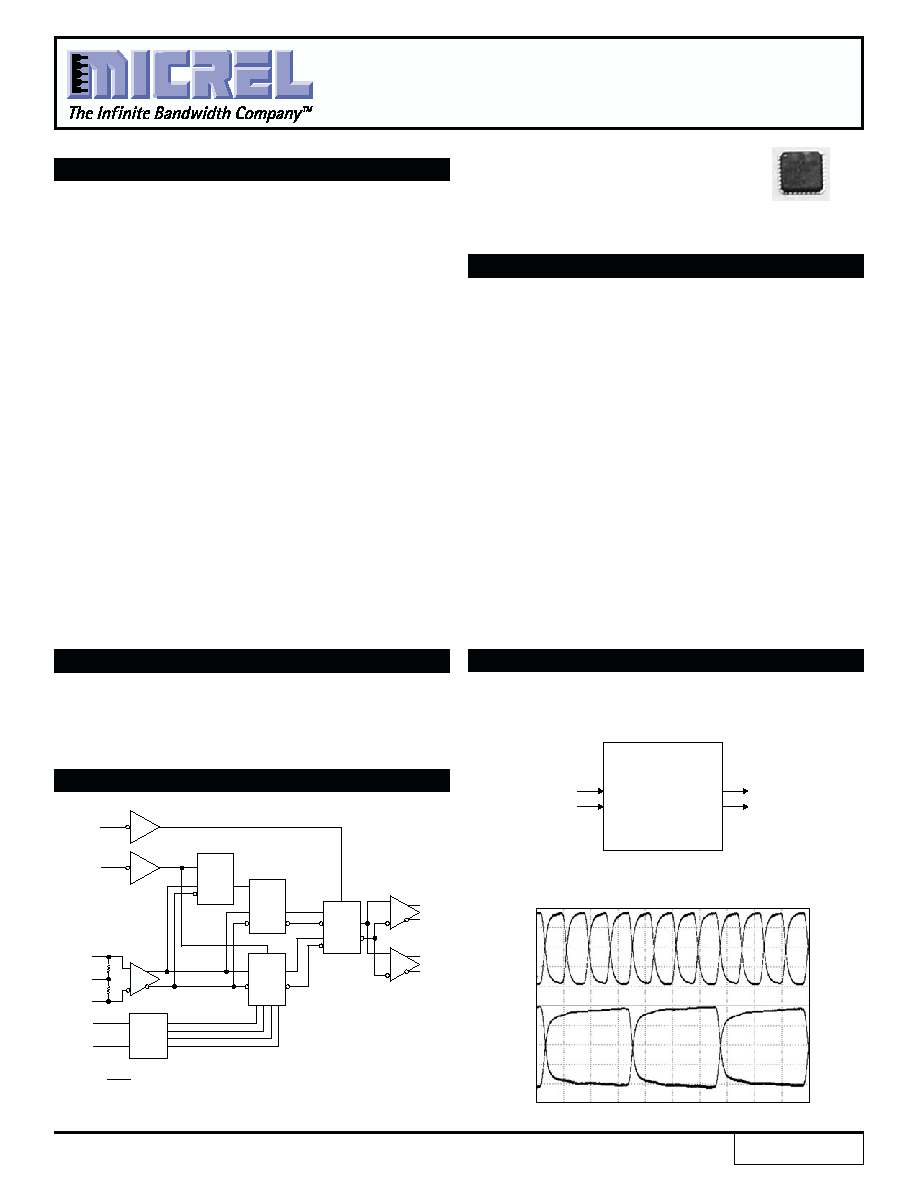
This low-skew, low-jitter device is capable of accepting a
high-speed (e.g., 622MHz or higher) CML, LVPECL, LVDS or
HSTL clock input signal and dividing down the frequency
using a programmable divider ratio to create a frequency-
locked, lower speed version of the input clock. Available divider
ratios are 2, 4, 8 and 16, or straight pass-through. In a typical
622MHz clock system this would provide availability of
311MHz, 155MHz, 77MHz or 38MHz auxiliary clock
components.
The differential input buffer has a unique internal termination
design that allows access to the termination network through
a V
T
pin. This feature allows the device to easily interface to
different logic standards. A V
REF-AC
reference is included for
AC-coupled applications.
The /RESET input asynchronously resets the divider. In
the pass-through function (divide by 1) the /RESET
synchronously enables or disables the outputs on the next
falling edge of IN (rising edge of /N).
FUNCTIONAL BLOCK DIAGRAM
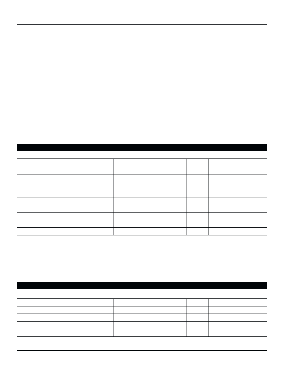
TYPICAL PERFORMANCE
Precision Edge is a trademark of Micrel, Inc.
MicroLeadFrame and MLF are trademarks of Amkor Technology, Inc.
IN
/IN
S0
S1
Q1
/Q1
Q0
/Q0
R0
R1
/RESET
V
T
V
REF-AC
S2
Divided
by
2, 4, 8
or 16
Enable
MUX
MUX
Enable
FF
Decoder
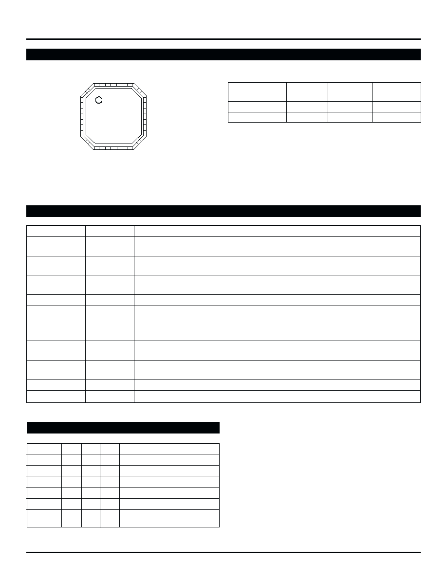
Divide-by-4
LVDS
622MHz
Clock In
OC-12 to OC-3
Translator/Divider
LVPECL
155.5MHz
Clock Out
622MHz In
/Q0
Q0
/IN
IN
155.5MHz Out
Precision EdgeTM
2
Precision EdgeTM
SY89874U
Micrel
PACKAGE/ORDERING INFORMATION
Ordering Information
Package
Operating
Package
Part Number
Type
Range
Marking
SY89874UMI
MLF-16
Industrial
874U
SY89874UMITR*
MLF-16
Industrial
874U
*Tape and Reel
Pin Number
Pin Name
Pin Function
12, 9
IN, /IN
Differential Input: Internal 50
termination resistors to V
T
input. Flexible input accepts any
differential input. See "Input Interface Applications" section.
1, 2, 3, 4
Q0, /Q0
Differential Buffered LVPECL Outputs: Divided by 1, 2, 4, 8 or 16. See "Truth Table."
Q1, /Q1
Unused PECL outputs may be left floating with no impact on jitter performance.
16, 15, 5
S0, S1, S2
Select Pins: See "Truth Table." LVTTL/CMOS logic levels. Internal 25k
pull-up
resistor. Logic HIGH if left unconnected (divided by 16 mode.) Input threshold is V
CC
/2.
6
NC
No Connect.
8
/RESET
LVTTL/CMOS Logic Levels: Internal 25k
pull-up resistor. Logic HIGH if left unconnected.
/DISABLE
Apply LOW to reset the divider (divided by 2, 4, 8 or 16 mode). Also acts as a synchronous
disable/enable function. The reset and disable function occurs on the next high-to-low
clock input transition. Input threshold is V
CC
/2.
10
VREF-AC
Reference Voltage: Equal to V
CC
≠1.4V (approx.). Used for AC-coupled applications only.
Decouple the V
REF-AC
pin with a 0.01
µF capacitor. See "Input Interface Applications" section.
11
VT
Termination Center-Tap: For CML or LVDS inputs, leave this pin floating. Otherwise, see
Figures 2a to 2f "Input Interface Applications" section.
7, 14
VCC
Positive Power Supply: Bypass with 0.1
µF//0.01µF low ESR capacitor.
13
GND
Ground.
PIN DESCRIPTION
1
2
3
4
12
11
10
9
16 15 14 13
5
6
7
8
Q0
/Q0
Q1
/Q1
IN
VT
VREF-AC
/IN
GND
VCC
S1
S0
/
RESET
VCC
NC
S2
16-Pin MLFTM (MLF-16)
/RESET
(1)
S2
S1
S0
Outputs
1
0
X
X
Reference Clock (pass through)
1
1
0
0
Reference Clock
˜2
1
1
0
1
Reference Clock
˜4
1
1
1
0
Reference Clock
˜8
1
1
1
1
Reference Clock
˜16
0
(1)
1
X
X
Q = LOW, /Q = HIGH
Clock Disable
Note 1.
Reset/Disable function is asserted on the next clock input
(IN, /IN) high-to-low transition.
TRUTH TABLE
3
Precision EdgeTM
SY89874U
Micrel
Note 1.
Permanent device damage may occur if ABSOLUTE MAXIMUM RATINGS are exceeded. This is a stress rating only and functional operation is
not implied at conditions other than those detailed in the operational sections of this data sheet. Exposure to ABSOLUTE MAXIMUM RATlNG
conditions for extended periods may affect device reliability.
Note 2.
The data sheet limits are not guaranteed if the device is operated beyond the operating ratings.
Note 3.
Due to the limited drive capability use for input of the same package only.
Note 4.
Junction-to-board resistance assumes exposed pad is soldered (or equivalent) to the device's most negative potential on the PCB.
Absolute Maximum Ratings
(Note 1)
Supply Voltage (V
CC
) .................................. ≠0.5V to +4.0V
Input Voltage (V
IN
) .................................. ≠0.5V to V
CC
+0.3
ECL Output Current (I
OUT
)
Continuous ......................................................... 50mA
Surge ................................................................ 100mA
Input Current IN,
/IN (I
IN
) ..........................................
±50mA
V
T
Current (I
VT
) ......................................................
±100mA
V
REF-AC
Sink/Source Current (I
VREF-AC
), Note 3 .......
±2mA
Lead Temperature (soldering 10 sec.) ...................... 220
∞C
Storage Temperature (T
S
) ....................... ≠65
∞C to +150∞C
Operating Ratings
(Note 2)
Supply Voltage (V
CC
) ................ +3.3V
±10% or +2.5V ±5%
Ambient Temperature (T
A
) ......................... ≠40
∞C to +85∞C
Package Thermal Resistance
MLFTM
(
JA
)
Still-Air ............................................................. 60
∞C/W
500lfpm ............................................................ 54
∞C/W
MLFTM
(
JB
), Note 4
Junction-to-Board ............................................ 32
∞C/W
T
A
= ≠40
∞C to +85∞C; Unless otherwise stated.
Symbol
Parameter
Condition
Min
Typ
Max
Units
V
CC
Power Supply
2.375
3.63
V
I
CC
Power Supply Current
No load, max. V
CC
50
75
mA
R
IN
Differential Input Resistance (IN, /IN)
80
100
120
V
IH
Input High Voltage (IN, /IN)
Note 3
0.1
≠
V
CC
+0.3
V
V
IL
Input Low Voltage (IN, /IN)
Note 3
≠0.3
≠
V
CC
+0.2
V
V
IN
Input Voltage Swing
Notes 3, 4
0.1
≠
3.6
V
V
DIFF_IN
Differential Input Voltage Swing
Notes 3, 4, 5
0.2
≠
V
|I
IN
|
Input Current (IN, /IN)
Note 3
≠
≠
45
mA
V
REF-AC
Reference Voltage
Note 6
V
CC
≠1.525 V
CC
≠1.425 V
CC
≠1.325
V
Note 1.
The circuit is designed to meet the DC specifications shown in the above table after thermal equilibrium has been established.
Note 2.
Specification for packaged product only.
Note 3.
Due to the internal termination (see
"Input Structures" ) the input current depends on the applied voltages at IN, /IN and V
T
inputs. Do not apply
a combination of voltages that causes the input current to exceed the maximum limit!
Note 4.
See
"Timing Diagram" for V
IN
definition. V
IN
(Max) is specified when V
T
is floating.
Note 5.
See
"Typical Operating Characteristics" section for V
DIFF
definition.
Note 6.
Operating using V
IN
is limited to AC-coupled PECL or CML applications only. Connect directly to V
T
pin.
DC ELECTRICAL CHARACTERISTICS
(Notes 1, 2)
V
CC
= 3.3V
±10% or 2.5V ±5%; T
A
= ≠40
∞C to +85∞C, R
L
= 50
to V
CC
≠2V; Unless otherwise stated.
Symbol
Parameter
Condition
Min
Typ
Max
Units
V
OH
Output High Voltage
V
CC
≠1.145 V
CC
≠1.020 V
CC
≠0.895
V
V
OL
Output Low Voltage
V
CC
≠1.945 V
CC
≠1.820 V
CC
≠1.695
V
V
OUT
Output Voltage Swing
550
800
1050
mV
V
DIFF_OUT
Differential Output Voltage Swing
1.10
1.60
2.10
V
Note 1.
The circuit is designed to meet the DC specifications shown in the above table after thermal equilibrium has been established.
Note 2.
Specification for packaged product only.
(100KEP) LVPECL DC ELECTRICAL CHARACTERISTICS
(Notes 1, 2)
4
Precision EdgeTM
SY89874U
Micrel
V
CC
= 3.3V
±10% or 2.5V ±5%; T
A
= ≠40
∞C to +85∞C; Unless otherwise stated.
Symbol
Parameter
Condition
Min
Typ
Max
Units
V
IH
Input HIGH Voltage
2.0
V
V
IL
Input LOW Voltage
0.8
V
I
IH
Input HIGH Current
≠125
20
µA
I
IL
Input LOW Current
≠300
µA
Note 1.
The circuit is designed to meet the DC specifications shown in the above table after thermal equilibrium has been established.
Note 2.
Specification for packaged product only.
LVTTL/CMOS DC ELECTRICAL CHARACTERISTICS
(Notes 1, 2)
5
Precision EdgeTM
SY89874U
Micrel
V
CC
= 3.3V
±10% or 2.5V ±5%; T
A
= ≠40
∞C to +85∞C; Unless otherwise stated.
Symbol
Parameter
Condition
Min
Typ
Max
Units
f
MAX
Maximum Output Toggle Frequency
Output Swing
400mV
2.5
GHz
Maximum Input Frequency
Divide by 2, 4, 8, 16
3.2
GHz
t
PLH
Differential Propagation Delay
Input Swing < 400mV
540
650
790
ps
t
PHL
IN to Q
Input Swing
400mV
480
600
730
ps
t
SKEW
Within-Device Skew (diff.)
Note 3
7
15
ps
Q0≠Q1
Part-to-Part Skew (diff.)
Note 3
250
ps
t
RR
Reset Recovery Time
Note 4
600
ps
T
jitter
Cycle-to-Cycle Jitter
Note 5
1
ps(rms)
Total Jitter
Note 6
10
ps(pk-pk)
t
r
,t
f
Rise/Fall Time (20% to 80%)
70
150
250
ps
Note 1.
Measured with 400mV input signal, 50% duty cycle, all outputs loaded with 50
to V
CC
≠2V, unless otherwise stated.
Note 2.
Specification for packaged product only.
Note 3.
Skew is measured between outputs under identical transitions.
Note 4.
See
"Timing Diagram."
Note 5.
Cycle-to-cycle jitter definition: the variation in period between adjacent cycles over a random sample of adjacent cycle pairs. T
jitter_cc
=T
n
≠T
n+1
,
where T is the time between rising edges of the output signal.
Note 6.
Total jitter definition: with an ideal clock input, of frequency
f
MAX
(device), no more than one output edge in 10
12
output edges will deviate by more
than the specified peak-to-peak jitter value.
AC ELECTRICAL CHARACTERISTICS
(Notes 1, 2)
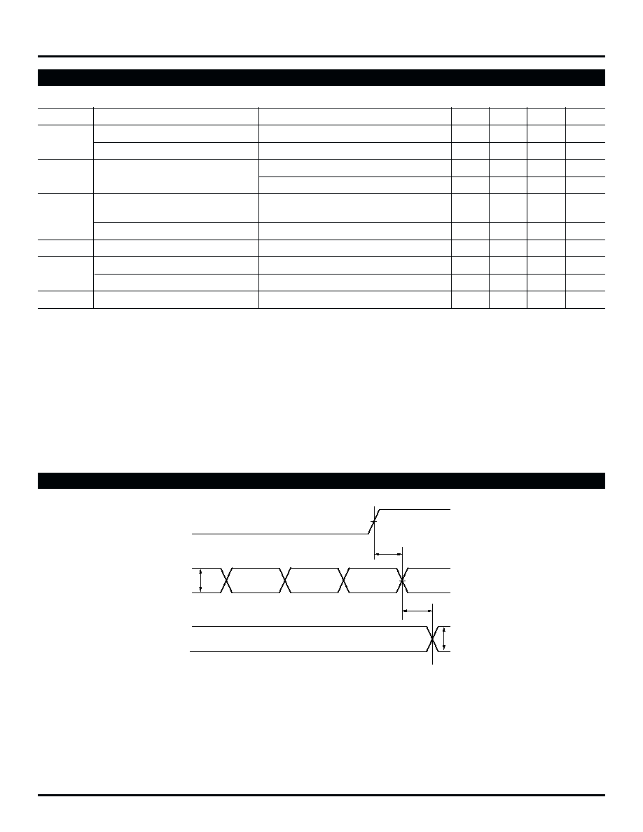
TIMING DIAGRAM
V
IN
/RESET
IN
/IN
/Q
Q
t
PD
t
RR
V
CC/2
V
IN
Swing
V
OUT
Swing