 | –≠–ª–µ–∫—Ç—Ä–æ–Ω–Ω—ã–π –∫–æ–º–ø–æ–Ω–µ–Ω—Ç: JAN117K | –°–∫–∞—á–∞—Ç—å:  PDF PDF  ZIP ZIP |

DESCRIPTION
The SG117A Series are 3-terminal positive adjustable voltage
regulators which offer improved performance over the original 117
design. A major feature of the SG117A is reference voltage
tolerance guaranteed within ± 1%, allowing an overall power supply
tolerance to be better than 3% using inexpensive 1% resistors. Line
and load regulation performance has been improved as well.
Additionally, the SG117A reference voltage is guaranteed not to
exceed 2% when operating over the full load, line and power
dissipation conditions. The SG117A adjustable regulators offer an
improved solution for all positive voltage regulator requirements
with load currents up to 1.5A.
FEATURES
∑∑
∑∑
∑ 1% output voltage tolerance
∑∑
∑∑
∑ 0.01%/V line regulation
∑∑
∑∑
∑ 0.3% load regulation
∑∑
∑∑
∑ Min. 1.5A output current
∑∑
∑∑
∑ Available in hermetic TO-220
HIGH RELIABILITY FEATURES-SG117A/SG117
Available to MIL-STD-883 and DESC SMD
MIL-M38510/11704BYA - JAN117K
MIL-M38510/11703BXA - JAN117T
LMI level "S" processing available
SG117A/SG217A/SG317A
SG117/SG217/SG317
1.5 AMP THREE TERMINAL
ADJUSTABLE VOLTAGE REGULATOR
SCHEMATIC DIAGRAM
2/93 Rev 1.
2 10/02
L
INFINITY
Microelectronics Inc.
Copyright
1994
11861 Western Avenue
Garden Grove, CA 92841
1
(714) 898-8121
FAX: (714) 893-2570
SG117A/SG117 SERIES
2/93 Rev 1.
2 10/02
L
INFINITY
Microelectronics Inc.
Copyright
1994
11861 Western Avenue
Garden Grove, CA 92841
2
(714) 898-8121
FAX: (714) 893-2570
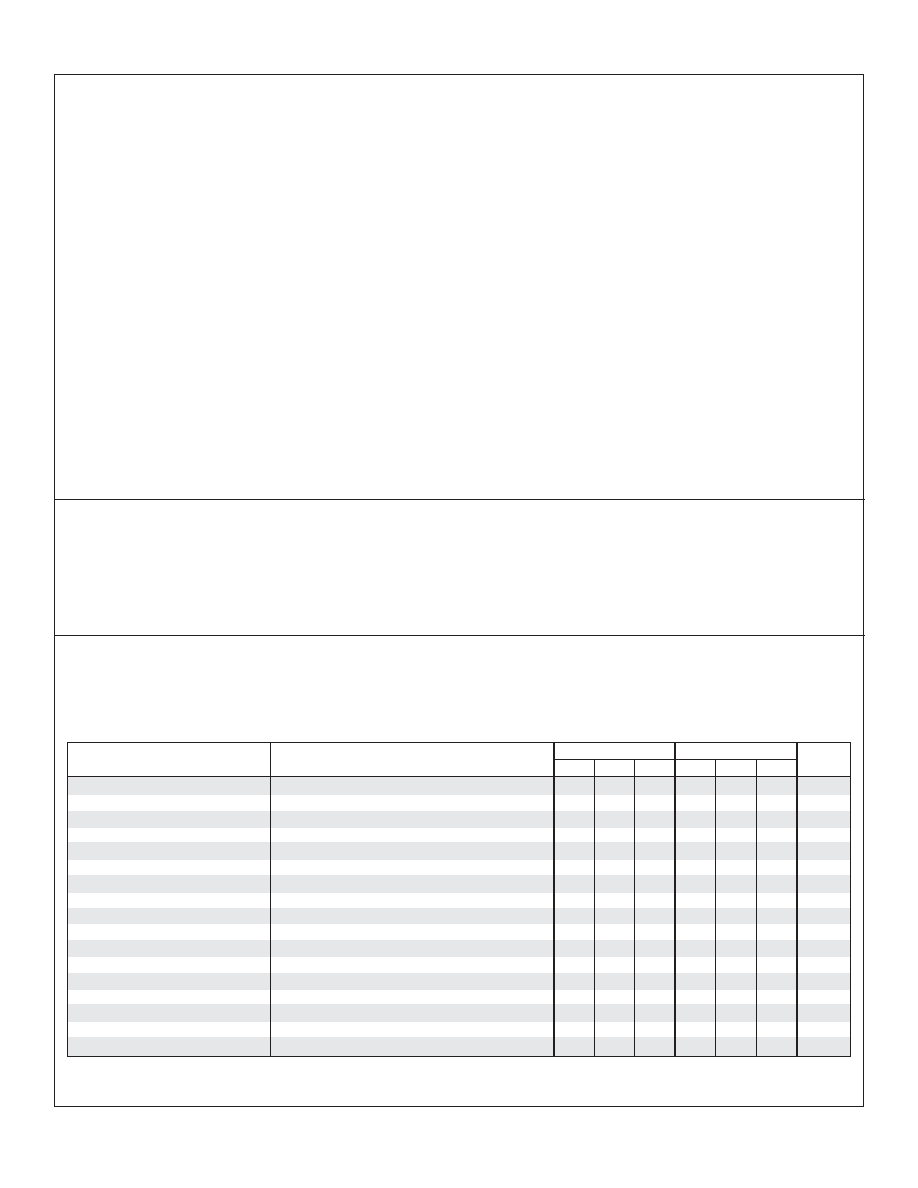
ELECTRICAL CHARACTERISTICS
(Unless otherwise specified, these specifications apply over full operating ambient temperatures for SG117A/SG117 with -55∞C
T
A
125∞C, SG217A/
SG217 with -25∞C
T
A
150∞C, SG 317A/SG317 with 0∞C T
A
125∞C, V
IN
- V
OUT
= 5.0V , and for I
OUT
= 500mA (K, R, and IG), and I
OUT
= 100mA
(T and L packages). Although power dissipation is internally limited, these specifications are applicable for power dissipations of 2W for the T and L
packages, and 20W for the K, R, and IG packages. I
MAX
is 1.5A for the K, R, and IG packages and 500mA for the T and L packages. Low duty cycle
pulse testing techniques are used which maintains junction and case temperatures equal to the ambient temperature.)
Power Dissipation ........................................
Input to Output Voltage Differential .................................
Storage Temperature Range ..........................
ABSOLUTE MAXIMUM RATINGS
(Note 1)
Internally Limited
40V
-65
∞C to 150∞C
Operating Junction Temperature
Hermetic (K, R, T, L, IG-Packages) ............................
Lead Temperature (Soldering, 10 Seconds) ..............
150
∞C
300
∞C
Note 1. Exceeding these ratings could cause damage to the device.
Input Voltage Range ..............................
(V
OUT
+ 3.5V) to 37V
Operating Junction Temperature Range
SG117A/SG117 .........................................
SG217A/SG217 .........................................
SG317A/SG317 ............................................
-55∞C to 150∞C
-25∞C to 150∞C
0∞C to 125∞C
Note 2. Range over which the device is functional.
Note 3. These ratings are applicable for junction temperatures of less than 150∞C.
RECOMMENDED OPERATING CONDITIONS
(Note 2 & 3)
Units
SG117/SG217
Min.
Typ. Max.
Min.
Typ. Max.
SG117A/SG217A
Parameter
Test Conditions
I
OUT
= 10mA T
A
= 25∞C
3V
(V
IN
- V
OUT
)
40V, P P
MAX
,
10mA
I
OUT
I
MAX
3V
(V
IN
- V
OUT
)
40V, I
L
= 10mA
T
A
= 25∞C
T
A
= T
MIN
to T
MAX
10mA
I
OUT
I
MAX
V
OUT
5V, T
A
= 25∞C
V
OUT
5V, T
A
= 25∞C
V
OUT
5V
V
OUT
5V
T
A
= 25∞C, 20ms pulse
V
OUT
= 10V, f =120Hz
C
ADJ
= 1
µF, T
A
= 25∞C
C
ADJ
= 10
µF
10mA
I
OUT
I
MAX
, 2.5V
(V
IN
- V
OUT
)
40V
1.238
1.225
66
1.250
1.250
0.005
0.01
5
0.1
20
0.3
0.002
65
80
50
0.2
1.262
1.270
0.01
0.02
15
0.3
50
1
0.02
100
5
1.20
66
1.25
0.01
0.02
5
0.1
20
0.3
0.03
65
80
50
0.2
1.30
0.02
0.05
15
0.3
50
1
0.07
100
5
V
V
%/V
%/V
mV
%
mV
%
%/W
dB
dB
µA
µA
K Package:
Thermal Resistance-
Junction to Case
,
JC
................. 3.0∞C/W
Thermal Resistance-
Junction to Ambient
,
JA
.............. 35∞C/W
R Package:
Thermal Resistance-
Junction to Case
,
JC
................. 5.0∞C/W
Thermal Resistance-
Junction to Ambient
,
JA
............. 40∞C/W
T Package:
Thermal Resistance-
Junction to Case
,
JC
.................. 15∞C/W
Thermal Resistance-
Junction to Ambient
,
JA
........... 120∞C/W
IG Package:
Thermal Resistance-
Junction to Case
,
JC
................. 3.5∞C/W
Thermal Resistance-
Junction to Ambient
,
JA
............. 42∞C/W
L Package:
Thermal Resistance-
Junction to Case
,
JC
.................. 35∞C/W
Thermal Resistance-
Junction to Ambient
,
JA
........... 120∞C/W
THERMAL DATA
Note A. Junction Temperature Calculation: T
J
= T
A
+ (P
D
x
JA
).
Note B. The above numbers for
JC
are maximums for the limiting
thermal resistance of the package in a standard mount-
ing configuration. The
JA
numbers are meant to be
guidelines for the thermal performance of the device/pc-
board system. All of the above assume no ambient
airflow.
Reference Voltage
Line Regulation
(Note 4)
Load Regulation
(Note 4)
Thermal Regulation
(Note 5)
Ripple Rejection
Adjust Pin Current
Adjust Pin Current Change
SG117A/SG117 SERIES
2/93 Rev 1.
2 10/02
L
INFINITY
Microelectronics Inc.
Copyright
1994
11861 Western Avenue
Garden Grove, CA 92841
3
(714) 898-8121
FAX: (714) 893-2570
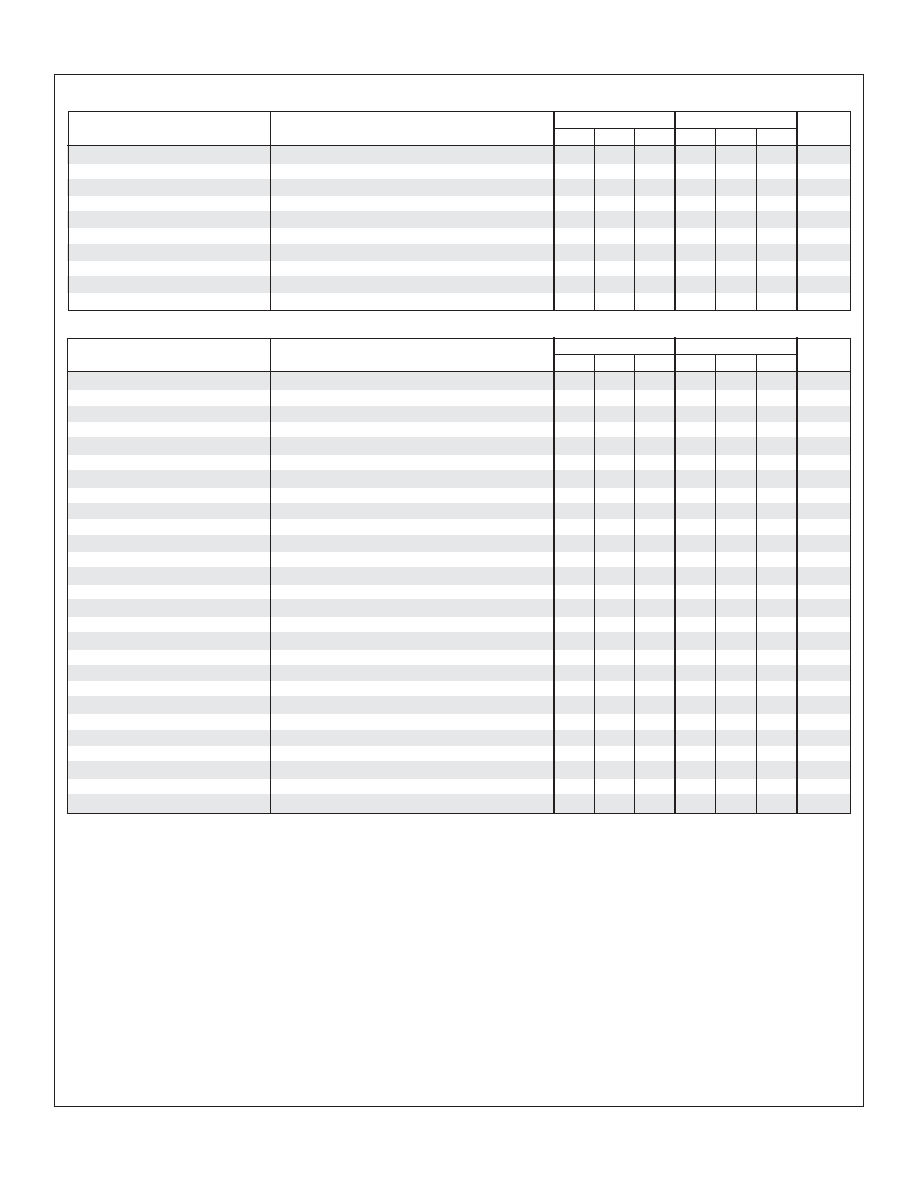
Units
Min.
Typ. Max.
Min.
Typ. Max.
1.262
1.270
0.01
0.02
25
0.5
50
1
0.02
100
5
10
2
1
1.25
0.01
0.02
5
0.1
20
0.3
0.03
65
80
50
0.2
3.5
2.2
0.8
0.4
0.2
1
0.3
0.001
1.30
0.04
0.07
25
0.5
70
1.5
0.07
100
5
10
1
Test Conditions
Parameter
Reference Voltage
Line Regulation
(Note 4)
Load Regulation
(Note 4)
Thermal Regulation
(Note 5)
Ripple Rejection
Adjust Pin Current
Adjust Pin Current Change
Minimum Load Current
Current Limit
Temperature Stability
(Note 5)
Long Term Stability
(Note 5)
RMS Output Noise (% of V
OUT
)
ELECTRICAL CHARACTERISTICS
(continued)
Test Conditions
Parameter
Units
SG117/SG217
Min.
Typ. Max.
Min.
Typ. Max.
SG117A/SG217A
(V
IN
- V
OUT
) = 40V
(V
IN
- V
OUT
)
15V
K, P, R, IG Packages
T, L Packages
(V
IN
- V
OUT
) = 40V, T
J
= 25∞C
K, P, R, IG Packages
T, L Packages
T
A
= 125∞C, 1000 Hours
T
A
= 25∞C,
10Hz
f 10 KHz
(Note 5)
1.5
0.5
0.3
0.15
5
2
1
3.5
2.2
0.8
0.4
0.2
1
0.3
0.001
1.5
0.5
0.3
0.15
3.5
2.2
0.8
0.4
0.2
1
0.3
0.001
5
1
mA
A
A
A
A
%
%
%
SG317A
SG317
I
OUT
= 10mA T
A
= 25∞C
3V
(V
IN
- V
OUT
)
40V, P P
MAX
,
10mA
I
OUT
I
MAX
3V
(V
IN
- V
OUT
)
40V, I
L
= 10mA
T
A
= 25∞C
T
A
= T
MIN
to T
MAX
10mA
I
OUT
I
MAX
V
OUT
5V, T
A
= 25∞C
V
OUT
5V, T
A
= 25∞C
V
OUT
5V
V
OUT
5V
T
A
= 25∞C, 20ms pulse
V
OUT
= 10V, f =120Hz
C
ADJ
= 1
µF, T
A
= 25∞C
C
ADJ
= 10
µF
T
A
= 25∞C
10mA
I
OUT
I
MAX
, 2.5V
(V
IN
- V
OUT
)
40V
(V
IN
- V
OUT
) = 40V
(V
IN
- V
OUT
)
15V
K, P, R, IG Packages
T, L Packages
(V
IN
- V
OUT
) = 40V, T
J
= 25∞C
K, P, R, IG Packages
T, L Packages
T
A
= 125∞C
T
A
= 25∞C,
10Hz
f 10KHz
(Note 5)
1.238
1.225
66
1.5
0.5
0.15
.075
1.250
1.250
0.005
0.01
5
0.1
20
0.3
0.002
65
80
50
0.2
3.5
2.2
0.8
0.4
0.2
1
0.3
0.001
1.20
66
1.5
0.5
0.15
.075
V
V
%/V
%/V
mV
%
mV
%
%/W
dB
dB
µA
µA
mA
A
A
A
A
%
%
%
Note 4. Regulation is measured at constant junction temperature, using pulse testing with a low duty cycle. Changes in output voltage due to
heating effects are covered under the specification for thermal regulation.
Note 5. These parameters, although guaranteed, are not tested in production.
Minimum Load Current
Current Limit
Temperature Stability
(Note 5)
Long Term Stability
(Note 5)
RMS Output Noise (% of V
OUT
)

SG117A/SG117 SERIES
2/93 Rev 1.
2 10/02
L
INFINITY
Microelectronics Inc.
Copyright
1994
11861 Western Avenue
Garden Grove, CA 92841
4
(714) 898-8121
FAX: (714) 893-2570
FIGURE 6.
QUISCENT CURRENT VS. INPUT/OUTPUT
DIFFERENTIAL
FIGURE 5.
REFERENCE VOLTAGE VS. TEMPERATURE
FIGURE 3.
ADJUSTMENT CURRENT VS. TEMPERATURE
FIGURE 2.
OUTPUT CURRENT VS. INPUT/OUTPUT
DIFFERENTIAL
FIGURE 1.
OUTPUT VOLTAGE DEVIATION VS. TEMPERATURE
FIGURE 4.
INPUT/OUTPUT DIFFERENTIAL VS. TEMPERATURE
FIGURE 9.
RIPPLE REJECTION VS. OUTPUT CURRENT
FIGURE 7.
RIPPLE REJECTION VS. OUTPUT VOLTAGE
FIGURE 8.
RIPPLE REJECTION VS. FREQUENCY
CHARACTERISTIC CURVES

SG117A/SG117 SERIES
2/93 Rev 1.
2 10/02
L
INFINITY
Microelectronics Inc.
Copyright
1994
11861 Western Avenue
Garden Grove, CA 92841
5
(714) 898-8121
FAX: (714) 893-2570
FIGURE 15.
LOAD TRANSIENT RESPONSE
FIGURE 14.
LINE TRANSIENT RESPONSE
FIGURE 13.
OUTPUT IMPEDANCE VS. FREQUENCY
FIGURE 12.
LOAD TRANSIENT RESPONSE
FIGURE 11.
LINE TRANSIENT RESPONSE
FIGURE 10.
OUTPUT IMPEDANCE VS. FEQUENCY
CHARACTERISTIC CURVES
(continued)
FIGURE 16.
OUTPUT VOLTAGE ERROR