 | –≠–ª–µ–∫—Ç—Ä–æ–Ω–Ω—ã–π –∫–æ–º–ø–æ–Ω–µ–Ω—Ç: ML2008CP | –°–∫–∞—á–∞—Ç—å:  PDF PDF  ZIP ZIP |
March 1997
ML2008
*
, ML2009
**
µ
P Compatible Logarithmic Gain/Attenuator
FEATURES
s
Low noise
0dBrnc max with +24dB gain
s
Low harmonic distortion
≠60dB max
s
Gain range
≠24 to +24dB
s
Resolution
0.1dB steps
s
Flat frequency response
±
0.05dB from 0.3-4kHz
±
0.10dB from 0.1-20kHz
s
Low supply current
4mA max from
±
5V supplies
s
TTL/CMOS compatible digital interface
s
ML2008 is designed to interface to an 8-bit data bus;
ML2009 to 16-bit data bus
GENERAL DESCRIPTION
The ML2008 and ML2009 are digitally controlled
logarithmic gain/attenuators with a range of ≠24 to +24dB
in 0.1dB steps.
Easy interface to microprocessors is provided by an input
latch and control signals consisting of chip select and
write.
The interface for gain setting of the ML2008 is by an 8-bit
data word, while the ML2009 is designed to interface to a
16-bit data bus with a single write operation by hard-
wiring the gain/attenuation pin or LSB pin. The ML2008
can be power downed by the microprocessor utilizing a
bit in the second write operation.
Absolute gain accuracy is 0.05dB max over supply
tolerance of
±
10% and temperature range.
These CMOS logarithmic gain/attenuators are designed for
* This Part Is End Of Life As Of August 1, 2000
a wide variety of applications in telecom, audio, sonar or
** This Part Is Obsolete
general purpose function generation.
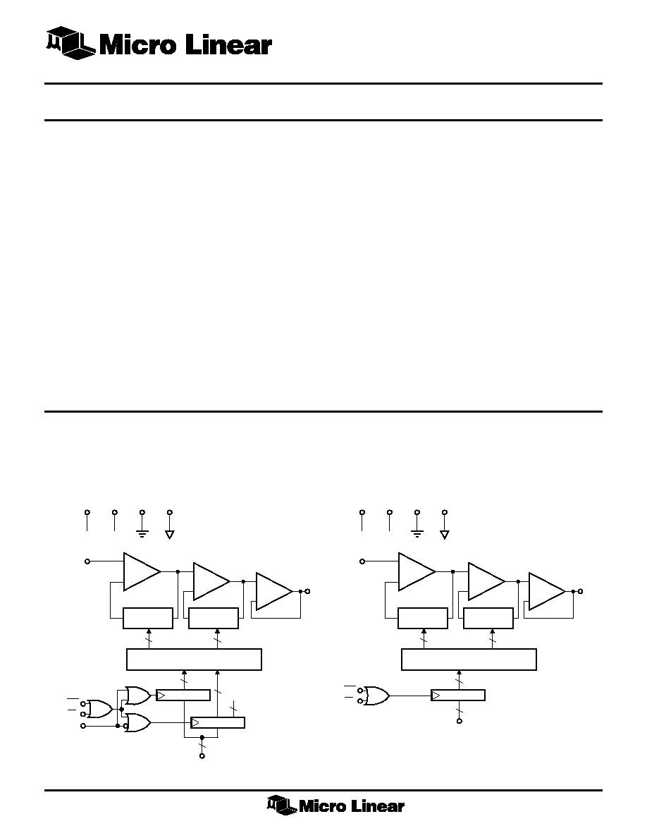
BLOCK DIAGRAM
+
≠
+
≠
+
≠
RESISTORS/
SWITCHES
RESISTORS/
SWITCHES
V
CC
V
SS
GND
AGND
V
IN
COARSE
FINE
BUFFER
V
OUT
16
16
+5
≠5
DECODERS
WR
CS
A0
REGISTER 0
REGISTER 1
8
1
1
PDN
D1≠D8
8
+
≠
+
≠
+
≠
RESISTORS/
SWITCHES
RESISTORS/
SWITCHES
V
CC
V
SS
GND
AGND
V
IN
COARSE
FINE
BUFFER
V
OUT
16
16
+5
≠5
DECODERS
REGISTER 0
9
D0≠D8
9
WR
CS
ML2008
ML2009
*
1
ML2008, ML2009
2
PIN CONFIGURATION
NAME
FUNCTION
V
SS
Negative supply. ≠5Volts
±
10%
V
CC
Positive supply. 5Volts
±
10%
GND
Digital ground. 0Volts. All digital
inputs are referenced to this ground.
AGND
Analog ground. 0Volts. Analog input
and output are referenced to this
ground.
V
IN
Analog input
V
OUT
Analog output
D8
Data bit, ATTEN/
GAIN
D7
Data bit, C3
D6
Data bit, C2
D5
Data bit, C1
D4
Data bit, C0
NAME
FUNCTION
D3
Data bit, F3
D2
Data bit, P
DN
, F2 ML2008; F2 ML2009
D1
Data bit, F0, F1 ML2008; F1 ML2009
D0
Data bit, F0 ML2009 only
WR
Write enable. This input latches the
data bits into the registers on rising
edges of
WR.
CS
Chip select. This input selects the
device by only allowing the
WR signal
to latch in data when
CS is low.
A0
Address select. This input determines
(ML2008 only)
which data word is being written into
the registers.
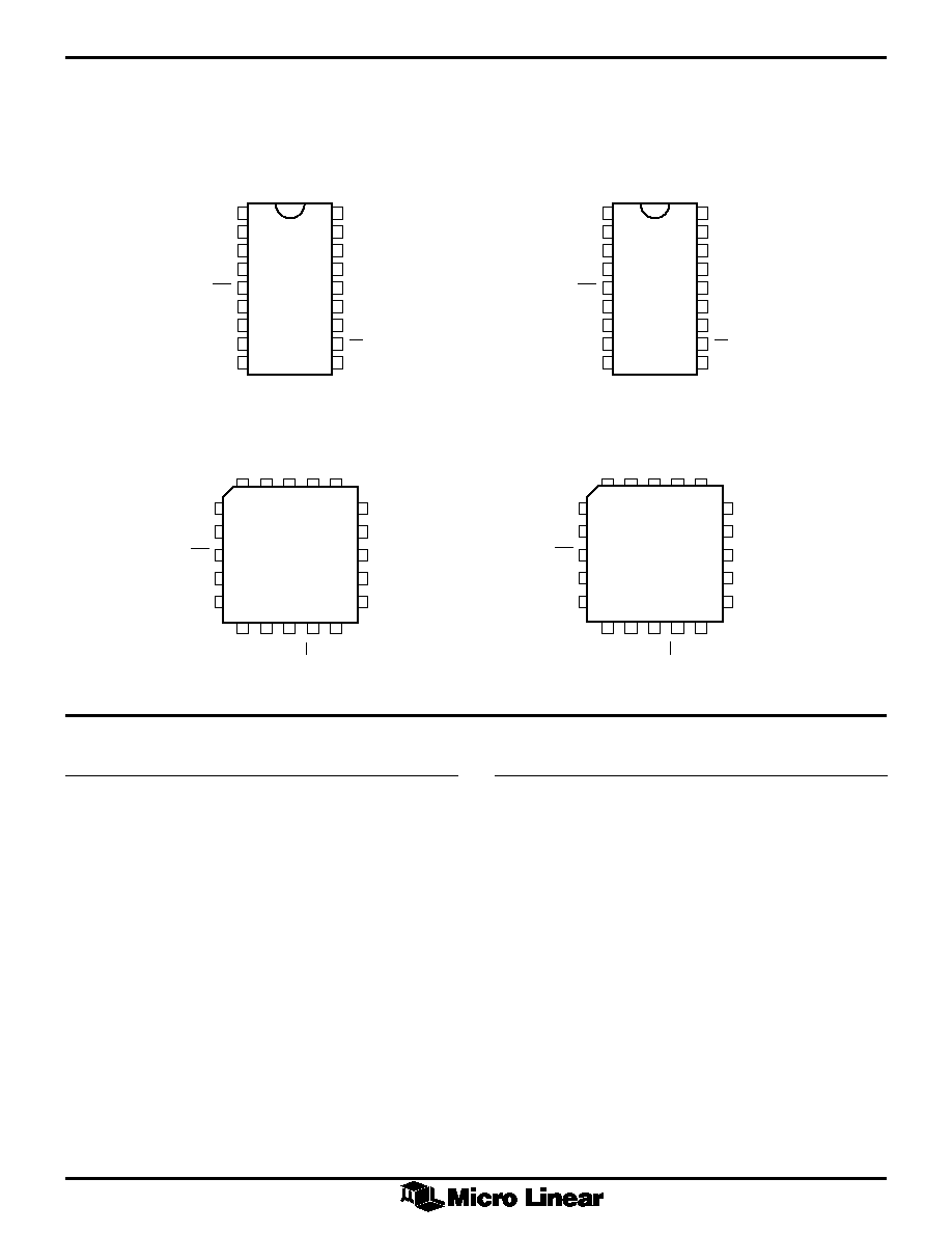
PIN DESCRIPTION
D7
D6
D5
D4
WR
D3
D2
D1
GND
D8
V
CC
V
OUT
V
SS
AGND
V
IN
NC
CS
A0
1
2
3
4
5
6
7
8
9
18
17
16
15
14
13
12
11
10
TOP VIEW
D8
V
CC
V
OUT
V
SS
AGND
V
IN
NC
CS
D0
1
2
3
4
5
6
7
8
9
18
17
16
15
14
13
12
11
10
TOP VIEW
V
OUT
V
SS
AGND
NC
NC
D4
NC
WR
D3
D2
9
10 11
12
13
D5
D6
D7
D8
V
CC
D1
GND
A0
CS
V
IN
4
5
6
7
8
3
2
1
20
19
18
17
16
15
14
TOP VIEW
V
OUT
V
SS
AGND
NC
NC
9
10 11
12
13
D5
D6
D7
D8
V
CC
D1
GND
D0
CS
V
IN
4
5
6
7
8
3
2
1
20
19
18
17
16
15
14
TOP VIEW
D4
NC
WR
D3
D2
D7
D6
D5
D4
WR
D3
D2
D1
GND
ML2008
18-Pin DIP (P18)
ML2009
*
18-Pin DIP (P18)
20-Pin PLCC (Q20)
20-Pin PLCC (Q20)

ML2008, ML2009
3
ABSOLUTE MAXIMUM RATINGS
(Note 1)
Supply Voltage
V
CC
.................................................................... +6.5V
V
SS
......................................................................≠6.5V
AGND with Respect to GND....................... V
CC
to V
SS
Analog Inputs and Outputs ..... V
SS
≠0.3V to V
CC
+0.3V
Digital Inputs and Outputs ... GND ≠0.3V to V
CC
+0.3V
Input Current Per Pin ........................................
±
25mA
Power Dissipation ........................................... 750mW
Storage Temperature Range ............... ≠65
∞
C to +150
∞
C
Lead Temperature (Soldering 10 sec.) ................. 300
∞
C
OPERATING CONDITIONS
Temperature Range (Note 2)
ML2008CX, ML2009CX .......................... 0
∞
C to +70
∞
C
ML2008IX, ML2009IX ......................... ≠40
∞
C to +85
∞
C
Supply Voltage
V
CC
................................................................ 4V to 6V
V
SS
............................................................. ≠4V to ≠6V
ELECTRICAL CHARACTERISTICS
Unless otherwise specified, T
A
= T
MIN
to T
MAX
, V
CC
= 5V
±
10%, V
SS
= ≠5V
±
10%, Data Word: D8 (ATTEN/
GAIN) = 1,
Other Bits = 0, (0dB Ideal Gain), C
L
= 100pF, R
L
= 600
, dBm measurements use 600
as reference load, digital timing
measured at 1.4V.
SYMBOL
PARAMETER
NOTES
CONDITIONS
MIN
TYP
MAX
UNITS
NOTE 3
Analog
AG
Absolute Gain Accuracy
4
V
IN
= 8dBm, 1kHz
≠0.05
+0.05
dB
RG
Relative Gain Accuracy
4
100000001
≠0.05
+0.05
dB
000000000
≠0.05
+0.05
dB
000000001
≠0.05
+0.05
dB
All other gain settings
≠0.1
+0.1
dB
All values referenced to 100000000
gain when D8 (ATTEN/
GAIN) = 1,
V
IN
= 8dBm when D8 (ATTEN/
GAIN) = 0,
V
IN
= (8dBm ≠ Ideal Gain) in dB
FR
Frequency Response
4
300-4000Hz
≠0.05
+0.05
dB
100-20,000Hz
≠0.1
+0.1
dB
Relative to 1kHz
V
OS
Output Offset Voltage
4
V
IN
= 0, +24dB gain
±
100
mV
I
CN
Idle Channel Noise
4
V
IN
= 0, +24dB, C msg weighted
≠6
0
dBrnc
5
V
IN
= 0, +24dB, 1kHz
450
900
nv/
Hz
HD
Harmonic Distortion
4
V
IN
= 8dBm, 1kHz
≠60
dB
Measure 2nd, 3rd, harmonic relative
to fundamental
SD
Signal to Distortion
4
V
IN
= 8dBm, 1kHz
+60
dB
C msg weighted
PSRR
Power Supply Rejection
4
200mV
P-P
, 1kHz sine, V
IN
= 0
on V
CC
≠60
≠40
dB
on V
SS
≠60
≠40
dB
Z
IN
Input Impedance, V
IN
4
1
Meg
V
INR
Input Voltage Range
4
±
3.0
V
V
OSW
Output Voltage Swing
4
±
3.0
V
ML2008, ML2009
4
ELECTRICAL CHARACTERISTICS
(Continued)
SYMBOL
PARAMETER
NOTES
CONDITIONS
MIN
TYP
MAX
UNITS
NOTE 3
Digital and DC
V
IL
Digital Input Low Voltage
4
0.8
V
V
IH
Digital Input High Voltage
4
2.0
V
I
IN
Input Current, Low
4
V
IH
= GND
≠10
µ
A
I
IN
Input Current, High
4
V
IH
= V
CC
10
µ
A
I
CC
V
CC
Supply Current
4
No output load, V
IL
= GND,
4
mA
V
IH
= V
CC
, V
IN
= 0
I
SS
V
SS
Supply Current
4
No output load, V
IL
= GND,
≠4
mA
V
IH
= V
CC
, V
IN
= 0
I
CCP
V
CC
Supply Current, ML2008
4
No output load, V
IL
= GND,
0.5
mA
Powerdown Mode Only
V
IH
= V
CC
I
SSP
V
SS
Supply Current, ML2008
4
No output load, V
IL
= GND,
≠0.1
mA
Powerdown Mode Only
V
IH
= V
CC
AC Characteristics
t
SET
V
OUT
Settling Time
4
V
IN
= 0.185V. Change gain from ≠24
20
µ
s
to +24dB. Measure from
WR rising
edge to when V
OUT
settles to within
0.05dB of final value.
t
STEP
V
OUT
Step Response
4
Gain = +24dB. V
IN
= ≠3V to +3V step.
20
µ
s
Measure from V
IN
= ≠3V to when V
OUT
settles to within 0.05dB of final value.
t
DS
Data Setup Time
4
50
ns
t
DH
Data Hold Time
4
50
ns
t
AS
A0 Setup Time
4
0
ns
t
AH
A0 Hold Time
4
0
ns
t
CSS
CS* Setup Time
4
0
ns
t
CSH
CS* Hold Time
4
0
ns
t
PW
WR* Pulse Width
4
50
ns
Note 1: Absolute maximum ratings are limits beyond which the life of the integrated circuit may be impaired. All voltages unless otherwise specified are measured with
respect to ground.
Note 2: 0
∞
C to +70
∞
C and ≠40
∞
C to +85
∞
C operating temperature range devices are 100% tested with temperature limits guaranteed by 100% testing, sampling, or by
correlation with worst-case test conditions.
Note 3: Typicals are parametric norm at 25
∞
C.
Note 4: Parameter guaranteed and 100% production tested.
Note 5: Parameter guaranteed. Parameters not 100% tested are not in outgoing quality level calculation.

ML2008, ML2009
5
TIMING DIAGRAM
D0-D8
A0
DATA
VALID
t
DS
t
DH
t
AH
t
AS
t
CSS
t
CSH
t
PW
CS
WR
TYPICAL PERFORMANCE CURVES
0
≠0.5
≠.10
≠.15
≠.20
≠.25
≠.30
≠.35
≠.40
≠.45
≠.50
100
1K
10K
100K
AMPLITUDE (dB)
FREQUENCY (Hz)
ATTEN: V
IN
= 0.5V
RMS
GAIN: V
IN
= 0.5V
RMS
/GAIN SETTING
GAIN = +24dB
GAIN = +18dB
GAIN = +12dB
GAIN = +0, ≠24dB
0
≠0.5
≠.10
≠.15
≠.20
≠.25
≠.30
≠.35
≠.40
≠.45
≠.50
100
1K
10K
100K
AMPLITUDE (dB)
FREQUENCY (Hz)
GAIN = +24dB
GAIN = 0dB
GAIN = ≠24dB
ATTEN: V
IN
= 2V
RMS
GAIN: V
IN
= 2V
RMS
/GAIN SETTING
2
1.8
1.6
1.4
1.2
1
0.8
0.6
0.4
0.2
0
10
100
1K
10K
OUTPUT NOISE
VOL
T
AGE (
µ
V/
Hz)
FREQUENCY (Hz)
GAIN = +24dB
GAIN = ≠24dB
GAIN = +12dB
Figure 4. Output Noise Voltage vs Frequency
Figure 5. C
MSG
Output Noise vs Gain Setting
≠2
≠3
≠4
≠5
≠6
≠7
≠8
≠9
≠10
≠24
C
MSG
OUTPUT (NOISE) (dBrnc)
GAIN SETTING (dB)
≠18
≠12
≠6
0
6
12
18
24
VIN = 0
Figure 3. Amplitude vs Frequency
(V
IN
/V
OUT
= 2V
RMS
)
Figure 2. Amplitude vs Frequency
(V
IN
/V
OUT
= 0.5V
RMS
)