 | –≠–ª–µ–∫—Ç—Ä–æ–Ω–Ω—ã–π –∫–æ–º–ø–æ–Ω–µ–Ω—Ç: ML2283CCP | –°–∫–∞—á–∞—Ç—å:  PDF PDF  ZIP ZIP |
May 1997
ML2280
*
, ML2283
**
Serial I/O 8-Bit A/D Converters
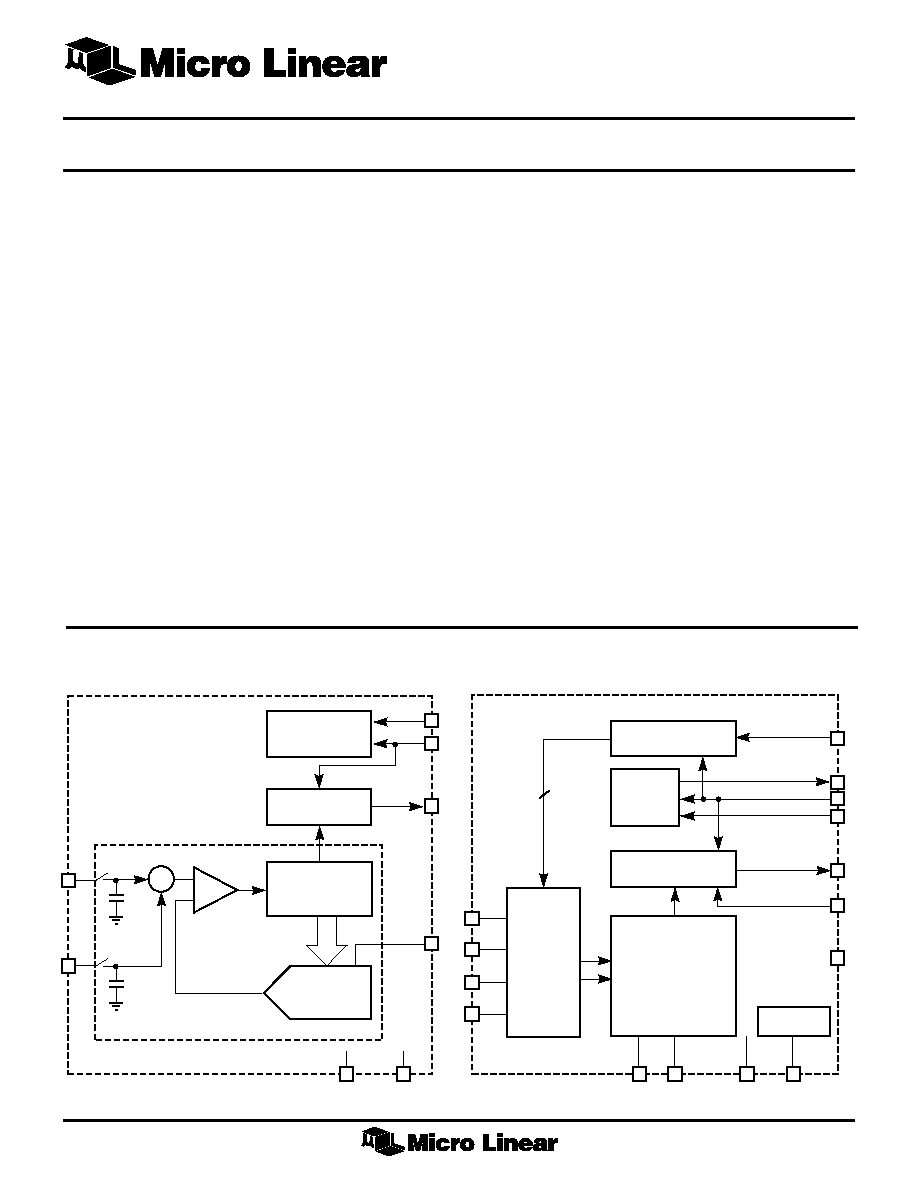
BLOCK DIAGRAM
1
GENERAL DESCRIPTION
The ML2280 and ML2283 are 8-bit successive
approximation A/D converters with serial I/O and
configurable input multiplexers with up to 4 input
channels.
All errors of the sample-and-hold incorporated on the
ML2280 and ML2283 are accounted for in the analog-to-
digital converters accuracy specification.
The voltage reference can be externally set to any value
between GND and V
CC
, thus allowing a full conversion
over a relatively small voltage span if desired.
The ML2283 is an enhanced double polysilicon, CMOS,
pin-compatible second source for the ADC0833 A/D
converter. All parameters are guaranteed over temperature
with a power supply voltage of 5V ±10%.
FEATURES
s
Conversion time: 6µs
s
ML2280 capable of digitizing a 5V, 40kHz sine wave
s
Total unadjusted error with external
reference: ±1/2LSB or ±1LSB
s
Sample-and-hold: 375ns acquisition
s
0 to 5V analog input range with single 5V
power supply
s
2.5V reference provides 0 to 5V analog input range
s
No zero- or full-scale adjust required
s
Low power: 12.5mW MAX
s
Analog input protection: 25mA (min) per input
s
Differential analog voltage inputs (ML2280)
s
Programmable multiplexer with differential or single
ended analog inputs (ML2283)
s
0.3" width 8- or 14-pin DIP, or 8-Pin SOIC (ML2280)
s
Superior pin-compatible replacement for ADC0833
INPUT
SHIFT-REGISTER
OUTPUT
SHIFT-REGISTER
SHUNT
REGULATOR
CONTROL
AND
TIMING
DI
SARS
CLK
CS
DO
4-BIT
SE
DGND
V+
V
CC
V
REF/2
AGND
CH3
CH2
CH1
CH0
A/D
CONVERTER
WITH
SAMPLE & HOLD
FUNCTION
4-CHANNEL
S.E.
OR
2-CHANNEL
DIFF
MULTIPLEXER
V
REF/2
CLK
CS
V
IN≠
SUCCESSIVE
APPROXIMATION
REGISTER
D/A
CONVERTER
+
≠
OUTPUT
SHIFT-REGISTER
CONTROL
AND
TIMING
COMP
A/D WITH SAMPLE & HOLD FUNCTION
8pF
8pF
≠
+
V
IN+
V
CC
GND
DO
ML2281
ML2283
* This Part Is Obsolete
** This Part Is End Of Life As Of August 1, 2000
ML2280, ML2283
2
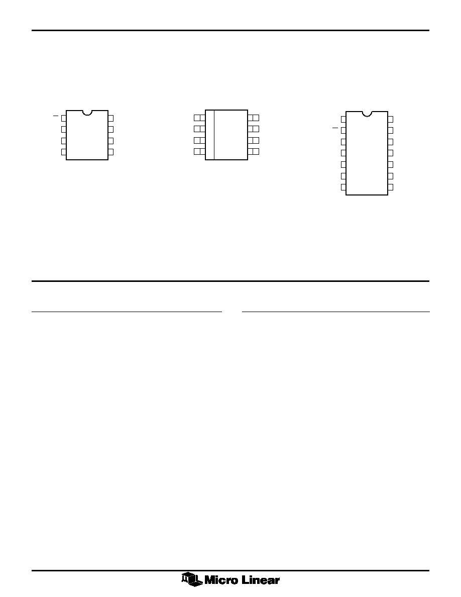
PIN CONFIGURATION
NAME
FUNCTION
V
CC
Positive supply. 5V ± 10%
DGND
Digital ground. 0 volts. All digital inputs and
outputs are referenced to this point.
AGND
Analog ground. The negative reference voltage
for A/D converter.
GND
Combined analog and digital ground.
CH0,
Analog inputs. Digitally selected to be single
V
IN
+, V
IN
≠ ended (V
IN
) or; V
IN
+ or V
IN
≠ of a differential
input. Analog range = GND - V
IN
- V
CC
.
V
REF/2
Reference. The analog input range is twice the
positive reference voltage value applied to this
pin.
V+
Input to the Shunt Regulator.
DO
Data out. Digital output which contains result
of A/D conversion. The serial data is clocked
out on falling edges of CLK.
PIN DESCRIPTION
ML2280
Single Differential Input
8-Pin PDIP
ML2283
4-Channel MUX
14-Pin PDIP
NAME
FUNCTION
SARS
Successive approximation register status.
Digital output which indicates that a
conversion is in progress. When SARS goes
to 1, the sampling window is closed and
conversion begins. When SARS goes to 0,
conversion is completed. When CS = 1, SARS
is in high impedance state.
CLK
Clock. Digital input which clocks data in on
DI on rising edges and out on DO on falling
edges. Also used to generate clocks for A/D
conversion.
DI
Data input. Digital input which contains serial
data to program the MUX and channel
assignments.
CS
Chip select. Selects the chip for multiplexer
and channel assignment and A/D conversion.
When CS = 1, all digital outputs are in high
impedance state. When CS = 0, normal A/D
conversion takes place.
CS
V
IN
+
V
IN
≠
GND
V
CC
CLK
DO
V
REF/2
1
2
3
4
8
7
6
5
TOP VIEW
TOP VIEW
V+
CS
CH0
CH1
CH2
CH3
DGND
V
CC
DI
CLK
SARS
DO
V
REF/2
AGND
1
2
3
4
5
6
7
8
9
10
11
12
13
14
ML2280
Single Differential Input
8-Pin SOIC
TOP VIEW
CS
V
IN
+
V
IN
≠
GND
V
CC
CLK
DO
V
REF/2
1
2
3
4
8
7
6
5
ML2280, ML2283
3
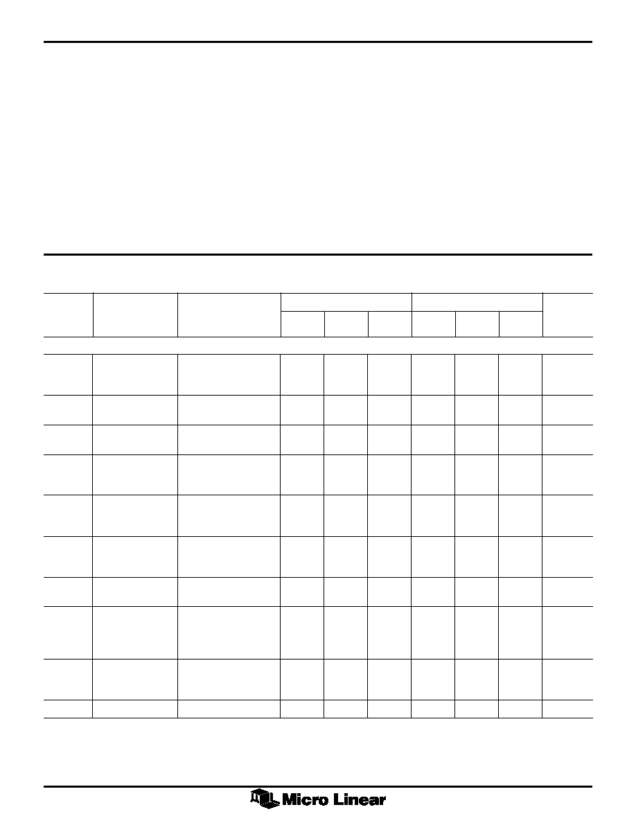
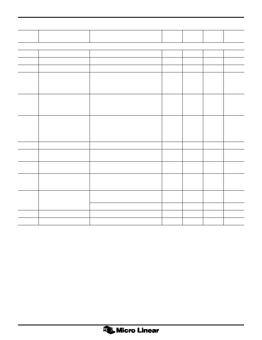
ELECTRICAL CHARACTERISTICS
Unless otherwise specified, T
A
= T
MIN
to T
MAX
, V
CC
= 5V ±10%, f
CLK
= 1.333MHz, and V
REF/2
= 2.5V.
ML228XB
ML228XC
TYP
TYP
SYMBOL
PARAMETER
CONDITIONS
MIN
NOTE 3
MAX
MIN
NOTE 3
MAX
UNITS
CONVERTER AND MULTIPLEXER CHARACTERISTICS
Total Unadjusted
V
REF/2
= 2.5V
±1/2
±1
LSB
Error
V
REF/2
not connected
±2
±2
LSB
(Notes 4, 6)
Reference Input
(Note 4)
10
15
20
10
15
20
k
W
Resistance
Common-Mode
(Notes 4, 7)
GND
V
CC
GND
V
CC
V
Input Range
≠0.05
+0.05
≠0.05
+0.05
DC Common-Mode Common mode voltage
±1/16
±1/4
±1/16
±1/4
LSB
Error
voltage GND to V
CC/2
(Note 5)
AC Common-Mode Common mode voltage
±1/4
±1/4
LSB
Error
GND to V
CC
,
0 to 50kHz (Note 5)
DC Power Supply
V
CC
= 5V ±10%
±1/32
±1/4
±1/32
±1/4
LSB
Sensitivity
V
REF
- V
CC
+0.1V
(Note 5)
AC Power Supply
100mV
P-P
, 25kHz sine
±1/4
±1/4
LSB
Sensitivity
on V
CC
(Note 5)
Change in Zero
15mA into V+
±1/2
±1/2
LSB
Error from V
CC
=5V
V
CC
= N.C.
to Internal Zener
V
REF/2
= 2.5V (Note 5)
Operation
V
Z
Internal Diode
15mA into V+
6.9
6.9
V
Regulated Break-
down (at V+)
V+
Input Resistance
(Note 4)
20
35
20
35
k
W
ABSOLUTE MAXIMUM RATINGS
Absolute maximum ratings are those values beyond which
the device could be permanently damaged. Absolute
maximum ratings are stress ratings only and functional
device operation is not implied.
Current into V+ ...................................................... 15mA
Supply Voltage, V
CC
................................................. 6.5V
Voltage
Logic Inputs ........................................... ≠7 to V
CC
+7V
Analog Inputs ................................ ≠0.3V to V
CC
+0.3V
Input Current per Pin (Note 1) .............................. ±25mA
Storage Temperature ................................ ≠65∞C to 150∞C
Package Dissipation
at T
A
= 25∞C (Board Mount) ............................. 800mW
Lead Temperature (Soldering 10 sec.)
Dual-In-Line Package (Molded) .......................... 260∞C
Dual-In-Line Package (Ceramic) ......................... 300∞C
OPERATING CONDITIONS
Supply Voltage, V
CC
............................ 4.5V
DC
to 6.3V
DC
Temperature Range (Note 2) ................. T
MIN
- T
A
- T
MAX
ML2280 BIP, ML2283 BIP ...................... ≠40∞C to 85∞C
ML2280 CIP, ML2283 CIP
ML2280 BCP, ML2283 BCP ...................... 0∞C to 70∞C
ML2280 CCP, ML2283 CCP
ML2280, ML2283
4
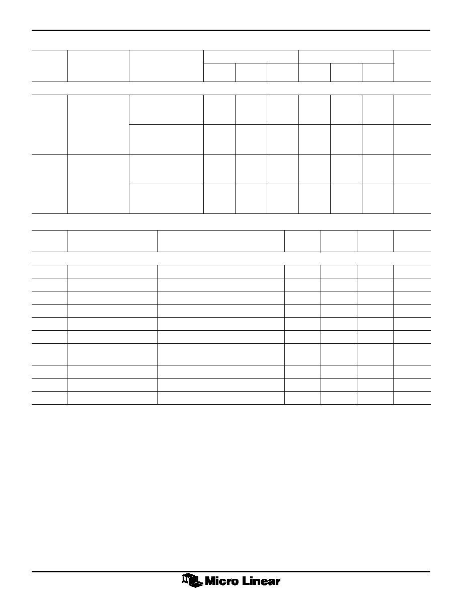
ELECTRICAL CHARACTERISTICS
(Continued)
ML228XB
ML228XC
TYP
TYP
SYMBOL
PARAMETER
CONDITIONS
MIN
NOTE 3
MAX
MIN
NOTE 3
MAX
UNITS
CONVERTER AND MULTIPLEXER CHARACTERISTICS (Continued)
I
OFF
Off Channel
On channel = V
CC
≠1
≠1
µA
Leakage Current
Off channel = 0V
(Notes 4, 8)
On channel = 0V
+1
+1
µA
Off channel = V
CC
(Notes 4, 8)
I
ON
On Channel
On channel = 0V
≠1
≠1
µA
Leakage Current
Off channel = V
CC
(Notes 4, 8)
On channel = V
CC
+1
+1
µA
Off channel = 0V
(Notes 4, 8)
TYP
SYMBOL
PARAMETER
CONDITIONS
MIN
NOTE 3
MAX
UNITS
DIGITAL AND DC CHARACTERISTICS
V
IN(1)
Logical "1" Input Voltage
(Note 4)
2.0
V
V
IN(0)
Logical "0" Input Voltage
(Note 4)
0.8
V
I
IN(1)
Logical "1" Input Current
V
IN
= V
CC
(Note 4)
1
µA
I
IN(0)
Logical "0" Input Current
V
IN
= 0V (Note 4)
≠1
µA
V
OUT(1
Logical "1" Output Voltage
I
OUT
= ≠2mA (Note 4)
4.0
V
V
OUT(0)
Logical "0" Output Voltage
I
OUT
= 2mA (Note 4)
0.4
V
I
OUT
HI-Z Output Current
V
OUT
= 0V (Note 4)
≠1
µA
V
OUT
= V
CC
1
µA
I
SOURCE
Output Source Current
V
OUT
= 0V (Note 4)
≠6.5
mA
I
SINK
Output Sink Current
V
OUT
= V
CC
(Note 4)
8.0
mA
I
CC
Supply Current
(Note 4)
1.3
2.5
mA
ML2280, ML2283
5
ELECTRICAL CHARACTERISTICS
(Continued)
TYP
SYMBOL
PARAMETER
CONDITIONS
MIN
NOTE 3
MAX
UNITS
AC ELECTRICAL CHARACTERISTICS
f
CLK
Clock Frequency
(Note 4)
10
1333
kHz
t
ACQ
Sample-and-Hold Acquisition
1/2
1/f
CLK
t
C
Conversion Time
Not including MUX adddressing time
8
1/f
CLK
SNR
Signal to Noise Ratio
V
IN
= 40kHz, 5V sine. f
CLK
= 1.333MHz
47
dB
ML2280
(f
SAMPLING
@ 120kHz). Noise is sum of all
nonfundamental components up to 1/2
of f
SAMPLING
(Note 11)
THD
Total Harmonic Distortion
V
IN
= 40kHz, 5V sine. f
CLK
= 1.333MHz
≠60
dB
ML2280
(f
SAMPLING
@ 120kHz). THD is sum of 2,
3, 4, 5 harmonics relative to fundamental
(Note 11)
IMD
Intermodulation Distortion
V
IN
= f
A
+ f
B
. f
A
= 40kHz, 2.5V sine.
≠60
dB
ML2280
f
B
= 39.8kHz, 2.5V Sine, f
CLK
= 1.333MHz
(f
SAMPLING
@ 120kHz). IMD is (f
A
+ f
B
),
(f
A
≠ f
B
), (2f
A
+ f
B
), (2f
A
≠ f
B
), (f
A
+ 2f
B
),
(f
A
≠ 2f
B
) relative to fundamental (Note 11)
Clock Duty Cycle
(Notes 4, 9)
40
60
%
t
SET-UP
CS Falling Edge or Data Input (Note 4)
130
ns
Valid to CLK Rising Edge
t
HOLD
Data Input Valid after
(Note 4)
80
ns
CLK Rising Edge
t
PD1
,
CLK Falling Edge to Output
C
L
= 100pF (Note 4 & 10)
t
PD0
Data Valid
Data MSB first
90
200
ns
Data LSB first
50
110
ns
t
1H
,
Rising Edge of CS to Data
C
L
= 10pF, R
L
= 10k
W (see high impedance
40
90
ns
t
0H
Output and SARS Hi-Z
test circuits) (Note 5)
C
L
= 100pF, R
L
= 2k
W (Note 5)
80
160
ns
C
IN
Capacitance of Logic Input
5
pF
C
OUT
Capacitance of Logic Outputs
5
pF
Note 1: When the input voltage (V
IN
) at any pin exceeds the power supply rails (V
IN
< GND < or V
IN
> V
CC
) the absolute value of current at that pin should be limited to
25mA or less.
Note 2: 0∞C to 70∞C and ≠40∞C to 85∞C operating temperature range devices are 100% tested with temperature limits guaranteed by 100% testing, sampling, or by
correlation with worst-case test conditions.
Note 3: Typicals are parametric norm at 25∞C.
Note 4: Parameter guaranteed and 100% tested.
Note 5: Parameter guaranteed. Parameters not 100% tested are not in outgoing quality level calculation.
Note 6: Total unadjusted error includes offset, full-scale, linearity, multiplexer and sample-and-hold errors.
Note 7: For V
IN
≠ ∑ V
IN
+ the digital output code will be 0000 0000. Two on-chip diodes are tied to each analog input (see Block Diagram) which will forward conduct for
analog input voltages one diode drop below ground or one diode drop greater than the V
CC
supply. Be careful, during testing at low V
CC
levels (4.5V), as high level
analog inputs (5V) can cause this input diode to conduct--especially at elevated temperatures, and cause errors for analog inputs near full-scale. The spec allows
50mV forward bias of either diode. This means that as long as the analog V
IN
or V
REF
does not exceed the supply voltage by more than 50mV, the output code will
be correct. To achieve an absolute 0V to 5V input voltage range will therefore require a minimum supply voltage of 4.950V
DC
over temperature variations, initial
tolerance and loading.
Note 8: Leakage current is measured with the clock not switching.
Note 9: A 40% to 60% clock duty cycle range insures proper operation at all clock frequencies. In the case that an available clock has a duty cycle outside of these limits,
the minimum time the clock is high or the minimum time the clock is low must be at least 300ns. The maximum time the clock can be high or low is 60µs.
Note 10: Since data, MSB first, is the output of the comparator used in the successive approximation loop, an additional delay is built in (see Block Diagram) to allow for
comparator response time..
Note 11: Because of multiplexer addressing, test conditions for the ML2283 is V
IN
= 30kHz, 5V sine (f
SAMPLING
™ 89kHz)