January, 2000
DATASHEET
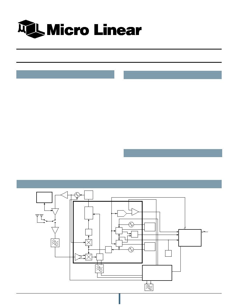
The ML2712 combined with the ML2713 form a FSK
(Frequency Shift Keying) 2.4 GHz radio chipset. The
ML2712 contains the RF and PLL circuits for a half duplex
radio transceiver solution for IEEE802.11 and other
wireless communication protocols using the 2.4 GHz ISM
band.
The ML2712 is controlled using a three-wire programming
interface and three control lines. The transmit circuits
feature an RF down converter for a transmit frequency
translation loop and a Wideband Phase Detector for a
directly modulated VCO transmitter. An RF down
converter mixer is provided for receive. All frequency
generation circuits are integrated for the RF conversion,
the 1LO VCO and PLL plus a 2LO VCO and PLL for use
in dual conversion radios. In addition the ML2712
contains an 8 bit D/A & Comparator that may be used
together as a tracking A/D for Received Signal Strength
Indication measurement (RSSI).
s
2.4GHz RF Down Converter
s
Programmable 2.2GHz and 236MHz Frequency
Synthesizers
s
External VCO tank circuits for flexibility
s
Compatibility with the OKI MSM7730 and similar
baseband controllers
s
Transmit Wideband Phase Comparator for closed loop
transmitter with >5MHz loop bandwidth
s
PLLs Programmable via 3 wire interface
s
48 pin TQFP 7mm body
s
3.0V to 5.5V operation
GENERAL DESCRIPTION
ML2712 2.4GHz RF Transceiver
FEATURES
ML2731
Bias
Controller
Transmit
Power
Amplifier
R. C.
Loop
Filter
LPF
MUX
+
�
DAC
Lock
Detect
2LO VCO
1LO VCO
x2
Tx Regulator
Output
2LO Loop
Filter &
Tank Circuit
1LO Loop
Filter &
Tank Circuit
32MHz
Clock
Baseband
Controller
(e.g., MSM7730B)
3
3
Reference
Frequency
Input
RSSI
Input
ML2712
ML2713
WB
Charge
Pump/WB
Phase
Comp
PLL 1
PLL 2
SIMPLIFIED BLOCK DIAGRAM
APPLICATIONS
s
2.4GHz Frequency Shift Key modulated radios
s
PC Card & Flashcard Wireless Transceivers
s
IEEE802.11FHSS Compatible 1 and 2Mbps Standard
PRELIMINARY

ML2712
2
January, 2000
PRELIMINARY
PRELIMINARY DATASHEET
TABLE OF CONTENTS
Micro Linear makes no representations or warranties with respect to the accuracy, utility, or completeness of the contents of
this publication and reserves the right to make changes to specifications and product descriptions at any time without notice.
No license, express or implied, by estoppel or otherwise, to any patents or other intellectual property rights is granted by this
document. The circuits contained in this document are offered as possible applications only. Particular uses or applications
may invalidate some of the specifications and/or product descriptions contained herein. The customer is urged to perform its
own engineering review before deciding on a particular application. Micro Linear assumes no liability whatsoever, and
disclaims any express or implied warranty, relating to sale and/or use of Micro Linear products including liability or warranties
relating to merchantability, fitness for a particular purpose, or infringement of any intellectual property right. Micro Linear
products are not designed for use in medical, life saving, or life sustaining applications.
General Description .........................................................................................................................................................1
Simplified Block Diagram ................................................................................................................................................1
Features ...........................................................................................................................................................................1
Applications .....................................................................................................................................................................1
Block Diagram ................................................................................................................................................................. 3
Pin Descriptions ...............................................................................................................................................................4
Pin Configuration .............................................................................................................................................................4
Functional Description ..................................................................................................................................................... 7
Introduction ................................................................................................................................................................7
Modes of Operation .........................................................................................................................................................8
Transmit Mode .............................................................................................................................................................8
Standby Mode .............................................................................................................................................................8
Receive Mode ........................................................................................................................................................... 10
Overview of PLLs ...................................................................................................................................................... 11
Operating Mode Control ............................................................................................................................................ 12
Serial Control Bus ...................................................................................................................................................... 13
Electrical Tables ............................................................................................................................................................... 18
Electrical Characteristics .................................................................................................................................................. 18
Absolute Maximum Ratings .............................................................................................................................................. 18
Operating Conditions ....................................................................................................................................................... 18
Physical Dimensions ........................................................................................................................................................ 24
Ordering Information ........................................................................................................................................................ 24
� Micro Linear 2000. is a registered trademark of Micro Linear Corporation. All other trademarks are the property of their
respective owners.
Products described herein may be covered by one or more of the following U.S. patents: 4,897,611; 4,964,026; 5,027,116;
5,281,862; 5,283,483; 5,418,502; 5,508,570; 5,510,727; 5,523,940; 5,546,017; 5,559,470; 5,565,761; 5,592,128; 5,594,376;
5,652,479; 5,661,427; 5,663,874; 5,672,959; 5,689,167; 5,714,897; 5,717,798; 5,742,151; 5,747,977; 5,754,012; 5,757,174;
5,767,653; 5,777,514; 5,793,168; 5,798,635; 5,804,950; 5,808,455; 5,811,999; 5,818,207; 5,818,669; 5,825,165; 5,825,223;
5,838,723; 5.844,378; 5,844,941. Japan: 2,598,946; 2,619,299; 2,704,176; 2,821,714. Other patents are pending.
WARRANTY
ML2712
3
January, 2000
PRELIMINARY
PRELIMINARY DATASHEET
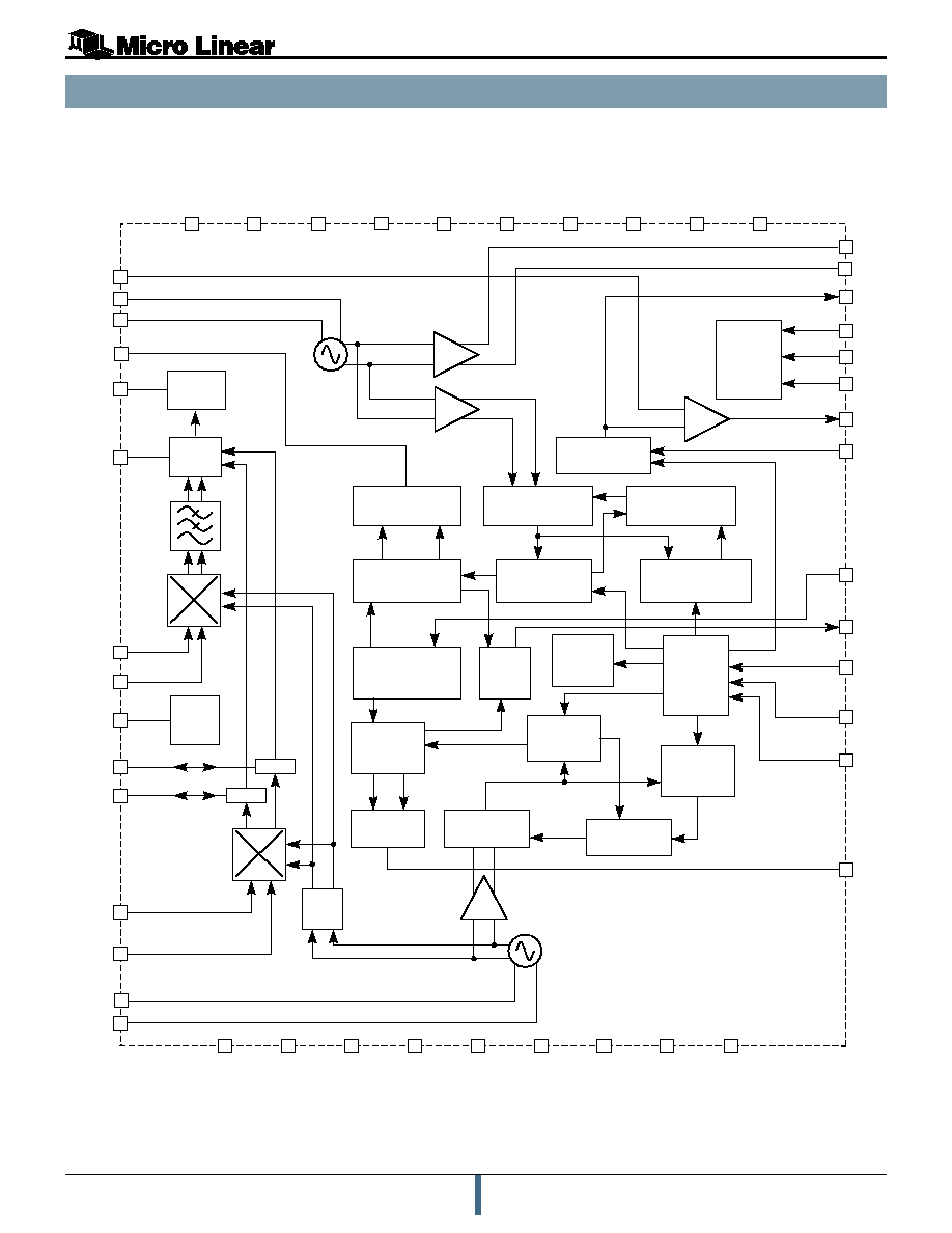
BLOCK DIAGRAM
35
4
WB
CHARGE
PUMP
CONTROL
8 BIT SERIAL
DAC
PRESCALER 14/15
2LO CHANGE
PUMP
2LO PHASE/
FREQUENCY
DETECTOR
REFERENCE
DIVIDER
2LO 5-BIT
COUNTER
LOCK
DETECT
CONTROL
2LO 4-BIT
SWALLOW COUNTER
1LO 6-BIT
COUNTER
1LO 6-BIT
SWALLOW
COUNTER
1LO PHASE/
FREQUENCY
DETECTOR
ADDRESS
DECODE
PRESCALER
CONTROL
WBCP
21
RVCC2
23
VCC7
27
VCC4
33
VCC8
34
VCC5
37
VCC6
16
VCC3
WBLD
22
BG
26
1IFB
25
1IF
32
TRFI
31
GND
WB
PHASE
COMP
BAND
GAP
REF
Rx
RF
MIXER
X2
MUX
MUX
1LO CHARGE
PUMP
PRESCALER
40/41
PRESCALER
CONTROL
30
RRFI
29
GND
LPF
Tx RF
MIXER
19
T1LO
1LO
VCO
9
GND
14
GND
17
GND
18
GND
24
GND
28
GND
36
GND
20
T1LOB
2LO
VCO
38
QP2
43
T2LO
RVCC3
2LO
2LOB
40
41
48 RS
47 TS
46 LOE
10 REF
8 DACEN
7 CLK
3 LD
6 DATA
5 EN
QP1
2 RSTH
45
RSSI
1 TPL
+
�
13
GND
44
GND
39
11
VCC1
12
RVCC1
15
VCC2
42
ML2712
4
January, 2000
PRELIMINARY
PRELIMINARY DATASHEET
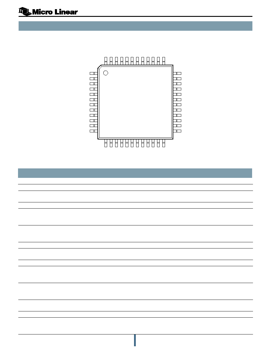
PIN DESCRIPTIONS
PIN CONFIGURATION
TOP VIEW
ML2712
48-Pin TQFP (H48-7)
GND
WBCP
VCC5
VCC8
TRFI
GND
RRFI
GND
GND
VCC4
1IFB
1IF
TPL
RSTH
LD
WBLD
EN
DATA
CLK
DACEN
GND
REF
VCC1
RVCC1
13 14 15
RS
TS
LOE
RSSI
GND
T2LO
RVCC
3
2LO
2LOB
GND
QP2
VCC
6
QP1
GND
VCC
2
VCC
3
GND
GND
T1LO
T1LOB
RVCC
2
BG
VCC
7
GND
16 17
1
2
3
4
5
6
7
8
9
10
11
12
36
35
34
33
32
31
30
29
28
27
26
25
18 19 20 21 22 23 24
48 47 46 45 44 43 42 41 40 39 38 37
Power and Ground
11
VCC
1
Supply Voltage for CMOS Logic. A bypass capacitor connected with minimum
trace lengths from VCC
1
to PCB ground is recommended
9
GND
Ground for CMOS Logic
15
VCC
2
Supply voltage for Digital/Analog Converter and Comparator. A bypass
capacitor connected with minimum trace lengths from VCC
2
to PCB ground is
recommended
16
VCC
3
Supply Voltage for 1LO Prescaler and Phase Detector. A bypass capacitor
connected with minimum trace lengths from VCC
3
to PCB ground is
recommended
17
GND
Ground for 1LO Prescaler and Phase Detector
27
VCC
4
Supply Voltage for RF Amplifier. A bypass capacitor connected with minimum
trace lengths from VCC
4
to PCB ground is recommended
28
GND
Ground for RF Low Noise Amplifier
34
VCC
5
Supply Voltage for Wideband Transmit PLL Charge Pump. A bypass capacitor
connected with minimum trace lengths from VCC
5
to PCB ground is
recommended
36
GND
Ground for Wideband Transmit PLL Charge Pump. Minimizing the lead trace
length from this GND to PCB ground to reduce inductance and resistance is
recommended
37
VCC
6
Supply Voltage for 2LO Charge Pump. A bypass capacitor connected with
minimum trace lengths from VCC
6
to PCB ground is recommended
39
GND
Ground for 2LO Charge Pump
23
VCC
7
Power Supply for 2LO Prescaler and Phase Detector. A bypass capacitor
connected with minimum trace lengths from VCC
7
to PCB ground is
recommended
Pin # Signal Name
I/O Type
Description

ML2712
5
January, 2000
PRELIMINARY
PRELIMINARY DATASHEET
PIN DESCRIPTIONS (continued)
24
GND
Ground for 2LO Prescaler and Phase Detector
33
VCC
8
Supply Voltage for Mixers, 1LO Frequency Doubler, and Transmit PLL. A
bypass capacitor connected with minimum trace lengths from VCC
8
to PCB
ground is recommended
29
GND
Ground for Mixers, 1LO Frequency Doubler, and Transmit PLL
Regulated Power and Ground
12
RVCC
1
Regulated Bypass Output Supply Voltage for 1LO PLL Charge Pump. A bypass
capacitor connected with minimum trace lengths from RVCC
1
to PCB ground is
recommended
14
GND
Ground for 1LO PLL Charge Pump
21
RVCC
2
Regulated Bypass Output Supply for 1LO Voltage Controlled Oscillator. A
bypass capacitor connected with minimum trace lengths from RVCC
2
to PCB
ground is recommended
18
GND
Ground for 1LO Voltage Controlled Oscillator
42
RVCC
3
Regulated Bypass Output Supply for 2LO Voltage Controlled Oscillator. A
bypass capacitor connected with minimum trace lengths from RVCC
3
to PCB
ground is recommended
44
GND
Ground for 2LO Voltage Controlled Oscillator
Transmitter Section
32
TRFI
I
Transmit RF Input signal. This signal, input to the Transmit Down Converter
Mixer should be AC coupled and matched to the nominal 50
Winput
impedance
31
GND
Transmit Signal Ground. Minimizing the lead trace length from this GND to
PCB ground to reduce inductance and resistance is recommended
35
WBCP
O (Analog)
Wideband PLL Charge Pump output
10
REF
I
Reference frequency input to Phase Locked Loops. Requires square wave input
3
LD
O (CMOS)
Lock Detect output. Low output indicates this pin is in open
drain. Two
Phase Locked Loops are frequency locked and requires 10k
W pull-up
4
WBLD
O (CMOS)
Wideband PLL Lock Detect open drain output and requires 10k
W pull-up
41
2LO
O
2LO output. Together with 2LOB provides a balanced 2LO output port for
input to Down Converter Mixer on ML2713. Requires 5K
W external pull-up
resistor to VCC3 if not connected to ML2713
In Standby Mode, 2LOB and 2LO provide a calibration tone used to calibrate
the ML2713 IF Transceiver
40
2LOB
O
2LOI output. Together with 2LO provide a balanced 2LO output port for input
to Down Converter Mixer on ML2713 Requires 5K
W external pull-up resistor to
VCC1 if not connected to ML2713
In Standby Mode, 2LO and 2LOB provide a calibration tone used to calibrate
the ML2713 IF Transceiver
25
1IF
I/O
IF Input/Output. In RECEIVE Mode, functions with 1IFB to present a balanced
first IF output port with 340
W output impedance. Connection must be AC
coupled. It is recommended that the signal trace connected to this pin be
isolated from other signal or digital control lines to maintain receiver
sensitivity
In TRANSMIT Mode, functions with 1IFB to present a balanced first IF input
port with 340
W input impedance. Connection must be AC coupled. It is
recommended that the signal trace connected to this pin be isolated from other
signal or digital control lines to maintain receiver sensitivity
Pin # Signal Name
I/O Type
Description