July 2000
PRELIMINARY
ML4769
*
2 Cell, Adjustable Output Boost Regulator
with Load Disconnect
1
GENERAL DESCRIPTION
The ML4769 is a continuous conduction boost regulator
designed for DC to DC conversion in multiple cell battery
power systems. Continuous conduction allows the
regulator to maximize output current for a given inductor.
The maximum switching frequency can exceed 200kHz,
allowing the use of small, low cost inductors. The ML4769
is capable of start-up with input voltages as low as 1.8V.
The output voltage can be set anywhere between 3.0V
and 5.5V by an external resistor divider connected to the
SENSE pin.
An integrated synchronous rectifier eliminates the need
for an external Schottky diode and provides a lower
forward voltage drop, resulting in higher conversion
efficiency. In addition, low quiescent current and variable
frequency operation result in high efficiency even at light
loads. The ML4769 requires only a few external
components to build a very small regulator capable of
achieving conversion efficiencies approaching 85%.
The SHDN input allows the user to stop the regulator from
switching, and provides complete isolation of the load
* Some Packages Are Obsolete
from the battery.
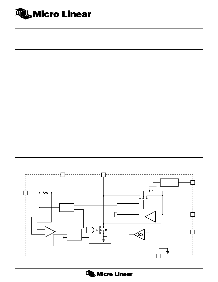
BLOCK DIAGRAM
FEATURES
s
Guaranteed full load start-up and operation at
1.8V input
s
Continuous conduction mode for high output current
s
Pulse Frequency Modulation and internal synchronous
rectification for high efficiency
s
Isolates the load from the input during shutdown
s
Minimum external components
s
Low ON resistance internal switching FETs
s
Low supply current
s
Adjustable output voltage (3V to 5.5V)
VL2
5
VOUT
4
SENSE
6
+
≠
SHUTDOWN
CONTROL
7
SHDN
VIN
2
2.57V
START-UP
3
GND
VL1
1
SYNCHRONOUS
RECTIFIER
CONTROL
BOOST
CONTROL
SHDN
+
≠
+
≠
8
PWR GND
ML4769
3
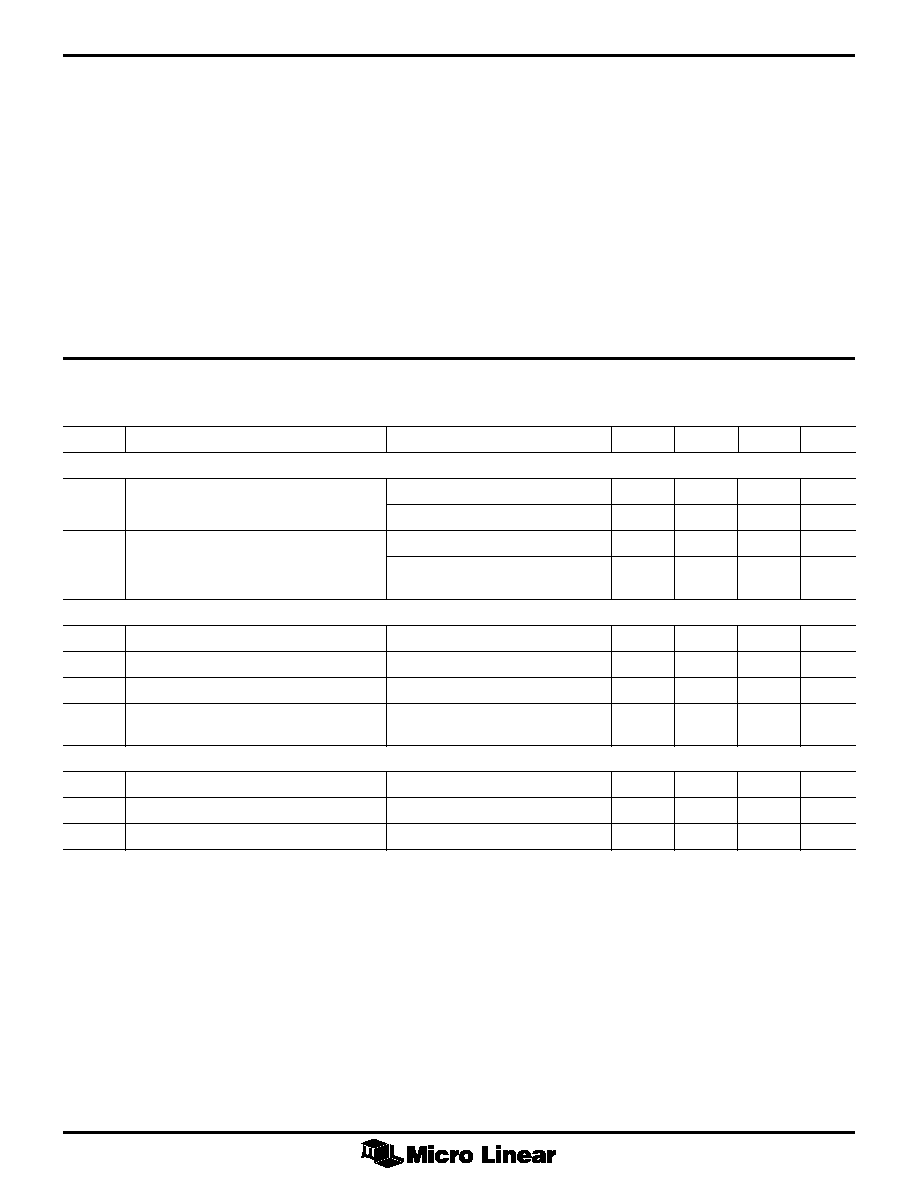
ELECTRICAL CHARACTERISTICS
Unless otherwise specified, V
IN
= Operating Voltage Range, T
A
= Operating Temperature Range (Note 1)
SYMBOL
PARAMETER
CONDITIONS
MIN
TYP
MAX
UNITS
SUPPLY
I
IN
V
IN
Current
V
IN
= V
OUT
- 0.2V, SHDN = 0V
3
6
µA
V
IN
= SHDN = 2.4V, V
OUT
= 0V
0.3
1
µA
I
OUT(Q)
V
OUT
Quiescent Current
SHDN = 0V
25
35
µA
V
IN
= SHDN = 2.4V,
14
20
µA
V
OUT
= V
OUT(NOM)
PFM REGULATOR
I
PEAK
I
L
Peak Current
750
850
950
mA
V
SENSE
SENSE Comparator Threshold Voltage
2.52
2.57
2.62
V
Line Regulation
I
OUT
= 0, See Figure 1
4.95
5.05
5.15
V
Load Regulation
V
IN
= 2.4V, I
OUT
£ 180mA
4.85
4.95
5.15
V
See Figure 1
SHUTDOWN
V
IL
Input Low Voltage
0.5
V
V
IH
Input High Voltage
V
IN
- 0.5
V
Input Bias Current
-100
100
nA
Note 1:
Limits are guaranteed by 100% testing, sampling, or correlation with worst case test conditions.
ABSOLUTE MAXIMUM RATINGS
Absolute maximum ratings are those values beyond
which the device could be permanently damaged.
Absolute maximum ratings are stress ratings only and
functional device operation is not implied.
V
OUT ...............................................................................................
7V
Voltage on any other pin ..... GND - 0.3V to V
OUT
+ 0.3V
Peak Switch Current (I
PEAK
) ......................................... 2A
Average Switch Current (I
AVG
) ..................................... 1A
Junction Temperature ............................................. 150∫C
Storage Temperature Range .................... ≠65∫C to 150∫C
Lead Temperature (Soldering, 10 sec) ................... 260∫C
Thermal Resistance (
q
JA
) .................................. 160∫C/W
OPERATING CONDITIONS
Temperature Range
ML4769CS-X .............................................. 0∫C to 70∫C
ML4769ES-X ........................................... -20∫C to 70∫C
V
IN
Operating Range ....................... 1.8V to V
OUT
- 0.2V
V
OUT
Operating Range ................................ 3.0V to 5.5V
ML4769
5
FUNCTIONAL DESCRIPTION
The ML4769 combines a unique form of current mode
control with a synchronous rectifier to create a boost
converter that can deliver high currents while maintaining
high efficiency. Current mode control allows the use of a
very small high frequency inductor and output capacitor.
Synchronous rectification replaces the conventional
external Schottky diode with an on-chip P-channel
MOSFET to reduce losses, eliminate an external
component, and provide the means for load disconnect.
Also included on-chip are an N-channel MOSFET main
switch and current sense resistor.
REGULATOR OPERATION
The ML4769 is a variable frequency, current mode
switching regulator. Its unique control scheme converts
efficiently over more than three decades of load current.
A block diagram of the boost converter including the key
external components is shown in Figure 2.
Error amp A3 converts deviations in the desired output
voltage to a small current, I
SET
. The inductor current is
measured through a current sense resistor (R
SENSE
) which
is amplified by A1. The boost control block matches the
average inductor current to a multiple of the I
SET
current
by switching Q1 on and off. The peak inductor current is
limited by the controller to about 900mA.
At light loads, I
SET
will momentarily reach zero after an
inductor discharge cycle, causing Q1 to stop switching.
Depending on the load, this idle time can extend to
tenths of a second. When the circuit is not switching, only
25µA of supply current is drawn from the output. This
allows the part to remain efficient even when the load
current drops below 250µA.
Amplifier A2 and the PMOS transistor Q2 work together
to form a low drop diode. When transistor Q1 turns off,
the current flowing in the inductor causes V
L2
to go high.
As the voltage on V
L2
rises above V
OUT
, amplifier A2
allows the PMOS transistor Q2 to turn on. In
discontinuous operation, (where I
L
always returns to zero),
A2 uses the resistive drop across the PMOS switch Q2 to
sense zero inductor current and turns the PMOS switch
off. In continuous operation, the PMOS turn off point is
independent of A2 and is determined by the boost control
circuitry.
Typical inductor current and voltage waveforms are
shown in Figure 3.
SHUTDOWN
The ML4769 output can be shut down by pulling the
SHDN pin high (to V
IN
). When SHDN is high, the
regulator stops switching, the control circuitry is powered
down, and the body diode of the PMOS synchronous
rectifier is disconnected from the output. By switching
Q1, Q2, and Q3 off, the load is isolated from the input.
This allows the output voltage to be independent of the
input while in shutdown.
DESIGN CONSIDERATIONS
OUTPUT CURRENT CAPABILITY
The maximum current available at the output of the
regulator is related to the maximum inductor current by
the ratio of the input to output voltage and the conversion
efficiency. The maximum inductor current is limited by
the boost controller to about 600mA. The conversion
efficiency is determined mainly by the internal switches
as well as the external components, but can be estimated
at about 80%. The maximum output current can be
determined by using the typical performance curves
shown in Figures 4 and 5, or by calculation using the
following equation:
I
V
V
V
A
OUT MAX
IN MIN
OUT
OUT
(
)
(
)
.
.
.
=
+
!
"
$
#
#
-
0 0392
0 488
0 144
1
6
2
7
(1)
Since the maximum output current is based on when the
inductor current goes into current limit, it is not
recommended to operate the ML4769 at the maximum
output current continuously. Applications that have high
transient load currents should be evaluated under worst
case conditions to determine suitability.
INDUCTOR SELECTION
The ML4769 is able to operate over a wide range of
inductor values. A value of 10µH is a good choice, but
any value between 5µH and 33µH is acceptable. As the
inductor value changes, the control circuitry will
automatically adjust to keep the inductor current under
control. Choosing an inductance value of less than 10µH
will reduce the component's footprint, but the efficiency
and maximum output current may drop.
It is important to use an inductor that is rated to handle
1.0A peak currents without saturating. Also look for an
inductor with low winding resistance. A good rule of
thumb is to allow 5 to 10m
W of resistance for each 1µH of
inductance.
The final selection of the inductor will be based on trade-
offs between size, cost and efficiency. Inductor tolerance,
core and copper loss will vary with the type of inductor
selected and should be evaluated with a ML4769 under
worst case conditions to determine its suitability.
Several manufacturers supply standard inductance values
in surface mount packages:
Coilcraft
(847) 639-6400
Coiltronics
(561) 241-7876
Dale
(605) 665-9301
Sumida
(847) 956-0666