 | –≠–ª–µ–∫—Ç—Ä–æ–Ω–Ω—ã–π –∫–æ–º–ø–æ–Ω–µ–Ω—Ç: ML4790CS | –°–∫–∞—á–∞—Ç—å:  PDF PDF  ZIP ZIP |

July 2000
ML4790
*
Adjustable Output, Low Ripple Boost Regulator
FEATURING
Extended Commercial Temperature Range
≠20∞C to 70∞C
for Portable Handheld Equipment
BLOCK DIAGRAM
1
GENERAL DESCRIPTION
The ML4790 is a high efficiency, PFM (Pulse Frequency
Modulation), boost switching regulator connected in
series with an integrated LDO (Low Dropout Regulator)
that incorporates "Silent SwitcherTM" technology. This
technique incorporates a patented tracking scheme to
minimize the voltage drop across the LDO and increase
the total efficiency of the regulator beyond that which can
be obtained by using a discrete external LDO regulator.
The ML4790 is designed to convert single or multiple cell
battery inputs to regulated output voltages for integrated
circuits and is ideal for portable communications
equipment that cannot tolerate the output voltage ripple
normally associated with switching regulators.
An integrated synchronous rectifier eliminates the need for
an external Schottky diode and provides a lower forward
voltage drop, resulting in higher conversion efficiency.
(* Indicates Part is End Of Life as Of July 1, 2000)
FEATURES
s
Incorporates "Silent SwitcherTM" technology to deliver
very low output voltage ripple (typically 5mV)
s
Guaranteed full load start-up and operation at 1.0V
input and low operating quiescent current (<100
µ
A)
for extended battery life
s
Pulse Frequency Modulation and internal synchronous
rectification for high efficiency
s
Minimum external components
s
Low ON resistance internal switching MOSFETs
s
Adjustable output voltage (2.5V to 5.5V)
Patent Pending
*Optional
BOOST
CONTROL
4
8
2
1
6
L1
SHDN
V
IN
GND
FEEDBACK
V
L
+
≠
V
OUT
PWR
GND
FROM
POWER
MANAGEMENT
*C
IN
V
BAT
7
LDO
CONTROL
5
V
BOOST
C2
V
OUT
3
SENSE
R
1
R
2
C
OUT
V
OUT
C
FB

2
ML4790
PIN CONNECTION
PIN DESCRIPTION
PIN
NO.
NAME
FUNCTION
1
V
IN
Battery input voltage
2
GND
Analog signal ground
3
SENSE
Programming pin for setting the
output voltage
4
V
OUT
LDO linear regulator output
ML4790
8-Pin SOIC (S08N)
PIN
NO.
NAME
FUNCTION
5
V
BOOST
Boost regulator output for connection
of an output filter capacitor
6
V
L
Boost inductor connection
7
SHDN
Pulling this pin high shuts down the
regulator, isolating the load from the
input
8
PWR GND Return for the NMOS boost transistor
V
IN
GND
SENSE
V
OUT
PWR GND
SHDN
V
L
V
BOOST
1
2
3
4
TOP VIEW
8
7
6
5

3
ML4790
Storage Temperature Range .................... ≠65
∞
C to +150
∞
C
Lead Temperature (Soldering 10s) .......................... +260
∞
C
Thermal Resistance (
JA
)
Plastic SOIC .................................................... 110
∞
C/W
OPERATING CONDITIONS
Temperature Range
ML4790CS-X ............................................ 0
∞
C to +70
∞
C
ML4790ES-X ......................................... ≠20
∞
C to +70
∞
C
V
IN
Range
ML4790CS-X ................................................ 1.0V to 6V
ML4790ES-X ................................................. 1.1V to 6V
V
OUT
Range .................................................. 2.5V to 5.5V
ABSOLUTE MAXIMUM RATINGS
Absolute maximum ratings are those values beyond which
the device could be permanently damaged. Absolute
maximum ratings are stress ratings only and functional
device operation is not implied.
V
BOOST
........................................................................ 7V
Voltage on Any Other Pin ... GND ≠0.3V to V
BOOST
+0.3V
Peak Switch Current (I
PEAK
) .......................................... 1A
Average Switch Current (I
AVG
) ............................... 500mA
LDO Output Current ............................................. 250mA
Junction Temperature .............................................. 150
∞
C
ELECTRICAL CHARACTERISTICS
Unless otherwise specified, V
IN
= Operating Voltage Range, T
A
= Operating Temperature Range. (Note 1)
PARAMETER
CONDITIONS
MIN
TYP.
MAX
UNITS
Supply
V
IN
Current
V
IN
= 6V
60
75
µ
A
SHDN = high
15
25
µ
A
V
OUT
Quiescent Current
V
BOOST
= V
OUT
+ 0.5V
8
10
µ
A
V
L
Quiescent Current
1
µ
A
PFM Regulator
Pulse Width (T
ON
)
4.5
5
5.5
µ
s
LDO
SENSE Comparator Threshold Voltage
194
200
206
mV
Load Regulation
See Figure 1
V
IN
= 1.2V, I
OUT
< 10mA
4.85
5.0
5.15
V
V
IN
= 2.4V, I
OUT
< 75mA
4.85
5.0
5.15
V
Dropout Voltage
See Figure 1
V
IN
= 1.2V, I
OUT
< 10mA
300
mV
V
IN
= 2.4V, I
OUT
< 75mA
500
mV
Output Ripple
5
mV
P-P
Shutdown
SHDN Threshold
0.5
0.8
1.0
V
SHDN Bias Current
≠100
100
nA
Note 1:
Limits are guaranteed by 100% testing, sampling, or correlation with worst case test conditions.
Figure 1. Application Test Circuit
ML4790
33
µ
F
V
IN
22
µ
H
(Sumida CD54)
V
OUT
V
IN
GND
SENSE
V
OUT
PWR GND
SHDN
V
L
V
BOOST
100
µ
F
I
OUT
100
µ
F
1nF
931k
39.2k
4
ML4790
FUNCTIONAL DESCRIPTION
The ML4790 combines Pulse Frequency Modulation
(PFM) and synchronous rectification to create a boost
converter that is followed by a low dropout linear
regulator (LDO). This combination creates a low output
ripple boost converter that is both highly efficient and
simple to use.
The PFM regulator charges a single inductor for a fixed
period of time and then completely discharges before
another cycle begins, simplifying the design by
eliminating the need for conventional current limiting
circuitry. Synchronous rectification is accomplished by
replacing an external Schottky diode with an on-chip
PMOS device, reducing switching losses and external
component count.
The integrated LDO reduces the output ripple voltage to
less than 5mV peak-to-peak. Integrating the LDO along
with the PFM regulator allows the circuit to be optimized
for very high efficiency using a patented feedback
technique. It also allows the LDO to provide the
maximum ripple rejection over the operating frequency
range of the regulator.
A block diagram of the ML4790 is shown in Figure 2. The
PFM stage is comprised of Q1, Q2, A1, A2, the one shot,
the flip-flop, and externals L1 and C2. The LDO stage is
comprised of Q3, A3, the offset voltage control, and
external components R1, R2 and C
OUT
. Since the LDO
actually controls the operation of the PFM regulator, the
operation of the LDO stage will be covered first.
LDO OPERATION
The LDO stage operates as a linear regulator. A3 is the
error amplifier, which compares the output voltage
through the divider R1 and R2 to the reference, and Q3 is
the pass device. When the output voltage is lower than
desired, the output of A3 increases the gate drive of Q3,
which reduces the voltage drop across it and brings the
output back into regulation. Similarly, if the output voltage
is higher than desired, A3 adjusts the gate drive of Q3 for
more drop and the output is brought back into regulation.
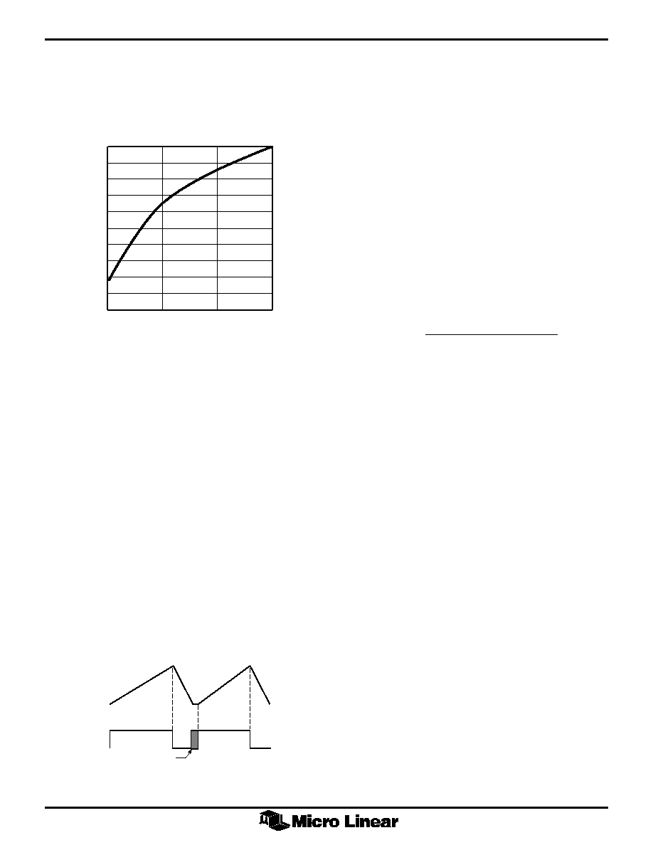
450
400
350
300
250
200
150
100
V
OS
(mV)
0
I
OUT
(mA)
10
20
30
40
50
60
70
80
90 100
Figure 3. LDO V
OS
versus output current.
Also included in the LDO stage is an offset voltage
control. This circuit monitors the output current and
adjusts the offset voltage according the general
characteristic shown in Figure 3. The offset control
ensures that the PFM stage provides just enough
"overhead" voltage for the LDO stage to operate properly.
+
≠
6
≠
5
µ
s
ONE SHOT
R
S
L1
Q3
A2
A1
Q1
R1
C
OUT
+
≠
+
5
C2
V
OS
= f (I
LOAD
)
+
≠
A3
V
REF
R2
4
I
LOAD
Q2
3
C
FB
Figure 2. PFM Regulator and LDO Block Diagram
5
ML4790
SHUTDOWN
The SHDN pin should be held low for normal operation.
Raising the voltage on SHDN above the threshold level
will release the gate of Q3, which effectively becomes an
open circuit. This also prevents the one shot from
triggering, which keeps switching from occurring.
DESIGN CONSIDERATIONS
INDUCTOR
Selecting the proper inductor for a specific application
usually involves a trade-off between efficiency and
maximum output current. Choosing too high a value will
keep the regulator from delivering the required output
current under worst case conditions. Choosing too low a
value causes efficiency to suffer. It is necessary to know
the maximum required output current and the input
voltage range to select the proper inductor value. The
maximum inductor value can be estimated using the
following formula:
L
V
T
V
V
I
MAX
IN MIN
ON MIN
OUT
OS
OUT MAX
=
◊
◊
◊
+
◊
(
)
(
)
(
)
(
)
2
2
(1)
where
is the efficiency, typically between 0.75 and
0.85, and V
OS
is the dropout voltage at I
OUT(MAX)
taken
from Figure 3. Note that this is the value of inductance
that just barely delivers the required output current under
worst case conditions. A lower value may be required to
cover inductor tolerance, the effect of lower peak inductor
currents caused by resistive losses, and minimum dead
time between pulses.
Another method of determining the appropriate inductor
value is to make an estimate based on the typical
performance curves given in Figures 6 and 7. Figure 6
shows maximum output current as a function of input
voltage for several inductor values. These are typical
performance curves and leave no margin for inductance
and ON-time variations. To accommodate worst case
conditions, it is necessary to derate these curves by at
least 10% in addition to inductor tolerance.
For example, a two cell to 5.5V application requires
40mA of output current while using an inductor with 15%
tolerance. The output current should be derated by 25%
to 50mA to cover the combined inductor and ON-time
tolerances. Assuming that 2V is the end of life voltage of a
two cell input, Figure 6 shows that with a 2V input, the
ML4790 delivers 52mA with a 22
µ
H inductor.
Note, that at lower output voltages there is less voltage
required at the PFM stage, and therefore less gate drive
available for the pass device Q3. This results in Q3 being
more resistive and unable to deliver as much output
current as a ML4790 set for a higher output voltage. This
characteristic is shown in Figure 4.
200
180
160
140
120
100
80
60
40
20
0
I
OUT
(mA)
2.5V
3.5V
4.5V
5.5V
V
OUT
(V)
Figure 4. ML4790 I
OUT
MAX
V
IN
= V
OUT
≠ 0.5V, L = 22
µ
H
PFM REGULATOR OPERATION
When the output of the PFM stage, V
BOOST
(pin 5), is at or
above the dropout voltage, V
OUT
+ V
OS
, the output of A1
stays low and the circuit remains idle. When V
BOOST
falls
below the required dropout voltage, the output of A1 goes
high, signaling the regulator to deliver charge to the
capacitor C2. Since the output of A2 is normally high, the
output of the flip-flop becomes SET. This triggers the one
shot to turn Q1 on and begins charging L1 for 5
µ
s. When
the one shot times out, Q1 turns off, allowing L1 to
flyback and momentarily charge C2 through the body
diode of Q2. But, as the source voltage of Q2 rises above
the drain, the current sensing amplifier A2 drives the gate
of Q2 low, causing Q2 to short out the body diode. The
inductor then discharges into C2 through Q2. The output
of A2 going low also serves to RESET the flip-flop in
preparation for the next charging cycle. When the
inductor current in Q2 falls to zero, the output of A2 goes
high, releasing Q2`s gate, allowing the flip-flop to be SET
again. If the voltage at V
BOOST
is still low, A1 will initiate
another pulse. Typical inductor current and voltage
waveforms are shown in Figure 5.
Q(ONE SHOT)
Q1 ON
Q1 ON
Q2
ON
Q2
ON
INDUCTOR
CURRENT
Q1 & Q2 OFF
Figure 5. PFM Inductor Current
Waveforms and Timing.