 | –≠–ª–µ–∫—Ç—Ä–æ–Ω–Ω—ã–π –∫–æ–º–ø–æ–Ω–µ–Ω—Ç: ML4811CP | –°–∫–∞—á–∞—Ç—å:  PDF PDF  ZIP ZIP |
1
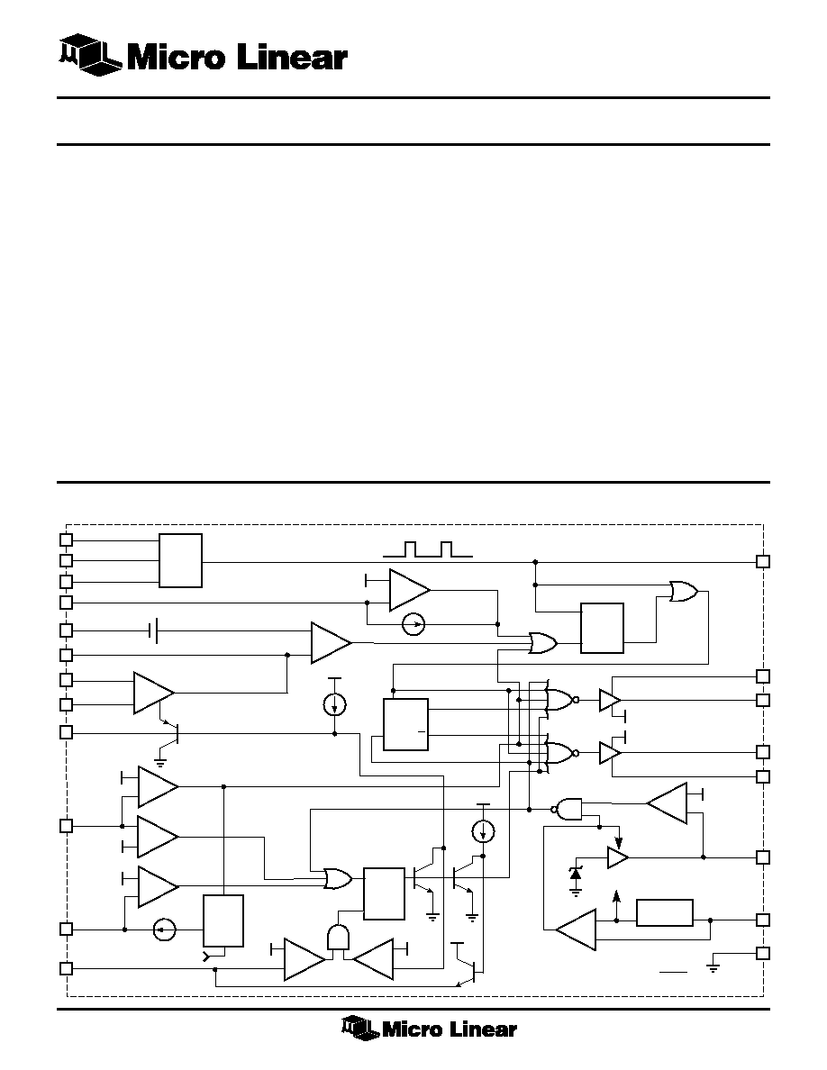
BLOCK DIAGRAM
(Pin numbers shown are for ML4811)
May 1997
ML4810
*
, ML4811
**
High Frequency Power Supply Controller
FEATURES
s
Integrating Soft Start Reset
s
High current (2A peak) dual totem pole outputs
s
Practical operation to 1MHz (f
OSC
)
s
5.1V
±
2% trimmed bandgap reference
s
Under voltage lockout with 7V hysteresis
s
Soft Start Reset Delay (ML4811)
s
Oscillator synchronization function (ML4811)
s
Soft Start latch ensures full soft start cycle
s
Outputs pull low for undervoltage lockout
s
Accurately controlled oscillator ramp discharge current
s
All timing currents "slaved" to R
T
for precise control
GENERAL DESCRIPTION
The ML4810 and ML4811 High Frequency PWM
Controllers are optimized for use in Switch Mode Power
Supply designs running at frequencies to 1MHz. The
ML4810/11 contain a unique overload protection circuit
which helps to limit stress on the output devices and
reliably performs a soft-start reset. These controllers are
designed to work in either voltage or current mode and
provide for input voltage feed forward.
A 1.1V threshold current limit comparator provides a
cycle-by-cycle current limit. An integrating circuit
"counts" the number of times the 1.1V limit was reached.
A soft-start cycle is initiated if the cycle-by-cycle current
limit is repeatedly activated. A reset delay function is
provided on the ML4811.
These controllers are similar to the UC1825 controller,
* This part is End of Life as of August 1, 2000
however these controllers include many features not
** This part is Obsolete
found on the 1825. These features are set in
Italics.
+
≠
R
T
OUT A
E/A OUT
I
LIM
/SD
RC (RESET)
RESET DELAY
INV
SOFT START
1.5V
CLOCK
1.1V
1.1V
5.1V
2.45V
1.1V
I(1)
3
◊
I(1)
V+
R
POWER V
C
POWER GND
P
4V
R
TF.F.
OSC
S
UNDER
VOLTAGE
LOCKOUT
INTERNAL
BIAS
Q
ENABLE
V
REF
V
REF
GEN
9V
Q
Q
C
Q
S
RAMP
C
T
CLOCK
PWR V
C
OUT B
POWER GND
V
CC
GND
NI
6
7
SYNC
10
O.V.P./SHUTDOWN
11
8
3
2
1
12
9
R
Q
S
+
≠
+
≠
+
≠
≠
+
4
20
≠
+
≠
+
≠
+
2.2V
1.5V V
REF
COMP
ERROR
AMP
1.25V
I(1)
V+
≠
+
≠
+
I(1) =
3V
16 x R
T
5
16
14
17
13
18
15
19

ML4810, ML4811
2
PIN CONFIGURATION
ML4810
16-Pin DIP (P16)
16-Pin SOIC (S16W)
PIN NAME
FUNCTION
PIN NAME
FUNCTION
1
INV
Inverting input to error amp.
2
NI
Non-inverting input to error amp.
3
E/A OUT
Output of error amplifier and input to
main comparator.
4
RC
RESET
Timing elements for Integrating Soft
Start reset.
5
CLOCK
Oscillator output.
6
R
T
Timing resistor for oscillator -- sets
charging current for oscillator timing
capacitor (pin 6).
7
C
T
Timing capacitor for oscillator.
8
RAMP
Non-inverting input to main
comparator. Connected to C
T
for
voltage mode operation or to current
sense resistor for current mode.
9
SOFT START Normally connected to Soft Start
capacitor.
10 SYNC
A high going pulse terminates the
PWM cycle and discharges C
T
.
PIN DESCRIPTION
11 OVP
Exceeding 2.5V terminates the PWM
cycle and inhibits the outputs.
12 I
LIM
/S.D.
Current limit sense pin. Normally
connected to current sense resistor.
13 GND
Analog signal ground.
14 OUTA
High current totem pole output. This
output is the first one energized after
power on reset.
15 PWR GND
Return for the high current totem
pole outputs.
16 V
C
Positive supply for the high current
totem pole outputs.
17 OUTB
High current totem pole output.
18 V
CC
Positive supply for the IC.
19 5.1V REF
Buffered output for the 5.1V voltage
reference.
20 RESET DELAY Timing capacitor to determine the
amount of delay between fault.
TOP VIEW
INV
NI
E/A OUT
RC
RESET
R
T
C
T
RAMP
SOFT START
5.1V REF
V
CC
OUTB
POWER V
C
PWR GND
OUTA
GND
I
LIM
/S.D.
1
2
3
4
5
6
7
8
16
15
14
13
12
11
10
9
ML4811
20-Pin DIP (P20)
20-Pin SOIC (S20)
INV
NI
E/A OUT
RC
RESET
CLOCK
R
T
C
T
RAMP
SOFT START
SYNC
RESET DELAY
5.1V REF
V
CC
OUTB
POWER V
C
PWR GND
OUTA
GND
I
LIM
/S.D.
OVP
1
2
3
4
5
6
7
8
9
10
20
19
18
17
16
15
14
13
12
11
TOP VIEW

ML4810, ML4811
3
ABSOLUTE MAXIMUM RATINGS
Absolute maximum ratings are those values beyond which
the device could be permanently damaged. Absolute
maximum ratings are stress ratings only and functional
device operation is not implied.
Supply Voltage (Pins 18, 16) ...................................... 25V
Output Current, Source or Sink (Pins 14, 17)
DC ....................................................................... 0.5A
Pulse (0.5
µ
s) ......................................................... 2.0A
Analog Inputs
(Pins INV, NI, SOFT START) ....................... ≠0.3V to 7V
(Pins 9, 10, 11, 12, 20) .............................. ≠0.3V to 6V
Clock Output Current (Pins 5) ................................. ≠5mA
Error Amplifier Output Current (Pin 3) ...................... 5mA
Junction Temperature ............................................. 150
∞
C
Storage Temperature Range ..................... ≠65
∞
C to 150
∞
C
Lead Temperature (Soldering 10 sec.) ..................... 260
∞
C
Thermal Resistance (
JA
)
Plastic DIP ....................................................... 65
∞
C/W
Plastic SOIC .................................................... 65
∞
C/W
ELECTRICAL CHARACTERISTICS
Unless otherwise specified, V
CC
= 15V, R
T
= 3.65k
, C
T
= 1000pF, T
A
= Operating Temperature Range. (Note 1)
PARAMETER
CONDITIONS
MIN
TYP
MAX
UNITS
OSCILLATOR
Initial Accuracy
T
J
= 25
∞
C
360
400
440
kHz
Voltage Stability
10V < V
CC
< 25V
0.2
4
%
Temperature Stability
5
%
Total Variation
line, temperature
340
460
kHz
Clock Out High
3.9
4.5
V
Clock Out Low
2.3
2.9
V
Ramp Peak
2.8
V
Ramp Valley
1.0
V
Ramp Valley to Peak
1.6
2.3
V
Sync Input Threshold
0.8
1.0
1.4
V
Sync Input Current
SYNC = 4V
µ
A
REFERENCE
Output Voltage
T
J
= 25
∞
C, I
O
= 1mA
5.00
5.10
5.20
V
Line Regulation
10V < V
CC
< 25V
2
20
mV
Load Regulation
1mA < I
O
< 10mA
5
20
mV
Temperature Stability
0
∞
C < T
J
< 150
∞
C
0.2
0.4
%
Total Variation
line, load, temperature
4.95
5.25
V
Output Noise Voltage
10Hz to 10kHz
50
µ
V
Long Term Stability
T
J
= 125
∞
C, 1000 hrs
5
25
mV
Short Circuit Current
V
REF
= 0V
≠15
≠50
≠100
mA
UNDERVOLTAGE LOCKOUT
Start Threshold
15
16
17
V
UVLO Hysteresis
6.5
7
7.5
V
ERROR AMPLIFIER
Input Offset Voltage
±
20
mV
Input Bias Current
0.6
3
µ
A
Input Offset Current
0.1
1
µ
A
Open Loop Gain
1 < V
O
< 4V
60
96
dB
OPERATING CONDITIONS
Temperature Range
ML4810, ML4811 ...................................... 0
∞
C to 70
∞
C
ML4810, ML4811
4
ELECTRICAL CHARACTERISTICS
(Continued)
PARAMETER
CONDITIONS
MIN
TYP
MAX
UNITS
ERROR AMPLIFIER (Continued)
CMRR
1.5 < V
CM
< 5.5V
65
95
dB
PSRR
10 < V
CC
< 30V
75
90
dB
Output Sink Current
V
PIN 3
= 1V
1
2.5
mA
Output Source Current
V
PIN 3
= 4V
≠0.5
≠1.3
mA
Output High Voltage
I
PIN 3
= ≠0.5mA
4.0
4.7
5.0
V
Output Low Voltage
I
PIN 3
= 1mA
0
0.5
1.0
V
Unity Gain Bandwidth
3
5.5
MHz
Slew Rate
6
12
V/
µ
s
PWM COMPARATOR
Pin 8 Bias Current
V
PIN 8
= 0V
≠1
≠5
µ
A
Duty Cycle Range
0
75
%
Pin 3 Zero DC Threshold
1.1
1.25
V
Delay to Output
50
80
ns
SOFT-START
Charge Current (Pin 9)
ML4811
V
PIN 9
= 1V, V
PIN 4
,
12
= 0
≠35
≠55
≠75
µ
A
Discharge Current (Pin 9)
V
PIN 9
= 3V, V
PIN 4
> 2.5
1
5
mA
V
PIN 9
= 3V, V
PIN 12
> 1.65, V
PIN 4
< 2
1
5
mA
Charge Current (Pin 20)
V
PIN 20
= 1V
1
5
mA
Discharge Current (Pin 20)
Requires external discharge resistor
0
µ
A
CURRENT LIMIT/SHUTDOWN
Pin 12 Bias Current
0V < V
PIN 12
< 4V
+15
µ
A
Current Limit Threshold
ML4810
1.2
1.3
1.4
V
ML4811
0.95
1.1
1.3
V
Reset Threshold (Pin 12)
ML4810
V
PIN 4
< 2V
1.60
1.75
1.90
V
ML4811
V
PIN 4
< 2V
1.4
1.50
1.8
V
Delay to Output
40
70
ns
Pin 4 Charging Current
V
PIN 12
= 2V
120
150
180
µ
A
Restart Threshold (Pin 4)
2
2.45
3
V
OVP Shutdown Threshold (Pin 11)
2.4
2.7
2.8
V
OVP Input Current
V
PIN 11
= 3V
40
50
60
µ
A
Charge Current (Pin 8)
ML4810
V
PIN 8
= 1V, V
PIN 4, 9
= 0
≠40
≠50
≠60
µ
A
OUTPUT
Output Low Level
I
OUT
= 20mA
0.25
0.4
V
I
OUT
= 200mA
1.2
2.2
V
Output High Level
I
OUT
= ≠20mA
13.0
13.5
V
I
OUT
= ≠200mA
12.0
13.0
V
Collector Leakage
V
C
= 30V
100
500
µ
A
Rise/Fall Time
C
L
= 1000pF
30
60
ns
SUPPLY
Start Up Current
ML4810
V
CC
= 8V
2.0
3.5
mA
ML4811
V
CC
= 8V
2.5
4.0
mA
I
CC
ML4810
V
PIN 1, 7, 9
= 0V, V
PIN 2
= 1V, T
A
= 25
∞
C
32
46
mA
ML4811
V
PIN 1, 7, 9
= 0V, V
PIN 2
= 1V, T
A
= 25
∞
C
38
55
mA
Note 1: Limits are guaranteed by 100% testing, sampling, or correlation with worst-case test conditions.
ML4810, ML4811
5
T
PD
T
PD
T
PD
V
TH2
SWITCH CURRENT
DIODE CURRENT
V
TH1
T
PD
T
PD
T
PD
V
TH2
SWITCH CURRENT
DIODE CURRENT
V
TH1
+
≠
+
≠
≠
+
≠
+
≠
+
≠
12
4
9
I
LIM
/SD
FROM OSC.
RC
RESET
ERROR
AMP
QI
Q2
F2
F3
F1
QI
G1
G2
I(2)
C1
I(1)
I(1)
R
R
Q
A5
A2
A4
A3
A1
4UL0
S
Q
S
R
1.5V
1.1V
S
Q
1.1V
2.45V
20
RESET DELAY
FROM OSC.
FROM PWM
COMPARATOR
SOFT START
V+
C2
R1
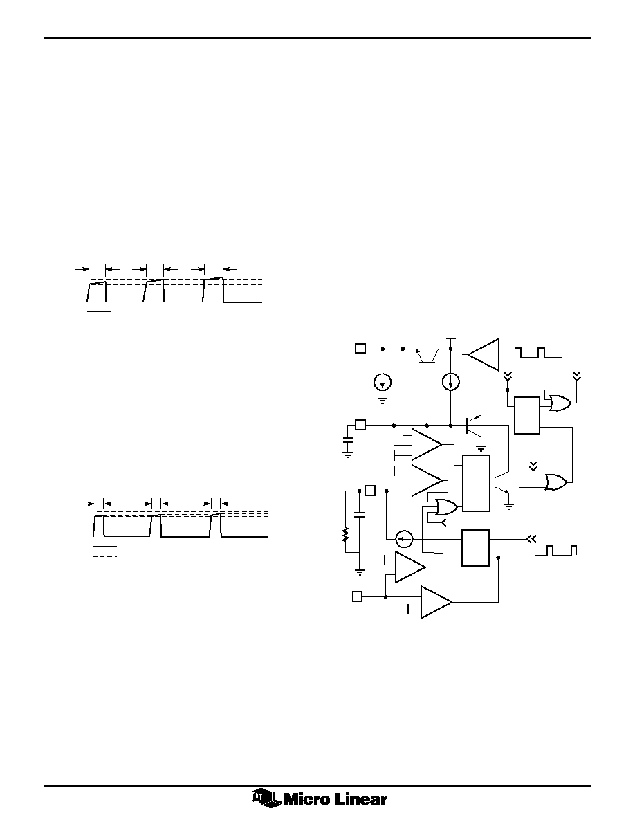
FUNCTIONAL DESCRIPTION
SOFT START AND CURRENT LIMIT
The ML4810/11 offers a unique system of fault detection
and reset. Most PWM controllers use a two threshold
method which relies on the buildup of current in the
output inductor during a fault. This buildup occurs
because:
1. Inductor di/dt is a small number when the switch is off
under load fault (short circuit) conditions, since VL is
small.
2. Some energy is delivered to the inductor since the IC
must first detect the over-current because there is a
finite delay before the output switch can turn off.
A method of circumventing this problem involves
"counting" the number of times the controller terminates
the PWM cycle due to the cycle by cycle current limit.
When the switch current crosses the 1.1V threshold A1
signals the F1 to terminate the cycle and sets F3, which is
reset at the beginning of the PWM cycle. The output of F3
turns on a current source to charge C2. When, after
several cycles, C2 has charged to 2.45V, A5 turns on F2 to
discharge soft start capacitor C1. Charge is short lived (for
instance a disk drive start-up or a board being plugged
into a live rack) the control can "ride out" the surge with
the switch protected by the cycle by cycle limit. R1 and
C1 can be selected to track diode heating, or to ride out
various system surge requirements as required.
If the high current demand is caused by a short circuit, the
duty cycle will be short and the output diodes will carry
the current for the majority of PWM cycle. C2 charges
fastest for low duty cycles (since F3 will be on for a longer
time) providing for quicker shutdown during short-circuit
when the output diodes are being maximally stressed.
Figure 1. Current Waveforms for Slow Turn-Off System
with Load Fault
This scheme was adequate for controllers with longer
comparator propagation delays and turn-off delays than is
desirable in a high frequency system. For systems with
low propagation delays, very little energy will be
delivered to the inductor and the current "ratcheting"
described above will not occur. This results in the
controller never detecting the load fault and continuing to
pump full current to the load indefinitely, causing heating
in the output rectifiers and inductor.
Figure 2. Current Waveforms for High Speed System
with Load Fault
Figure 3. Integrating Soft Start Reset