 | –≠–ª–µ–∫—Ç—Ä–æ–Ω–Ω—ã–π –∫–æ–º–ø–æ–Ω–µ–Ω—Ç: ML4825CP | –°–∫–∞—á–∞—Ç—å:  PDF PDF  ZIP ZIP |
1
May 1997
ML4825
*
High Frequency Power Supply Controller
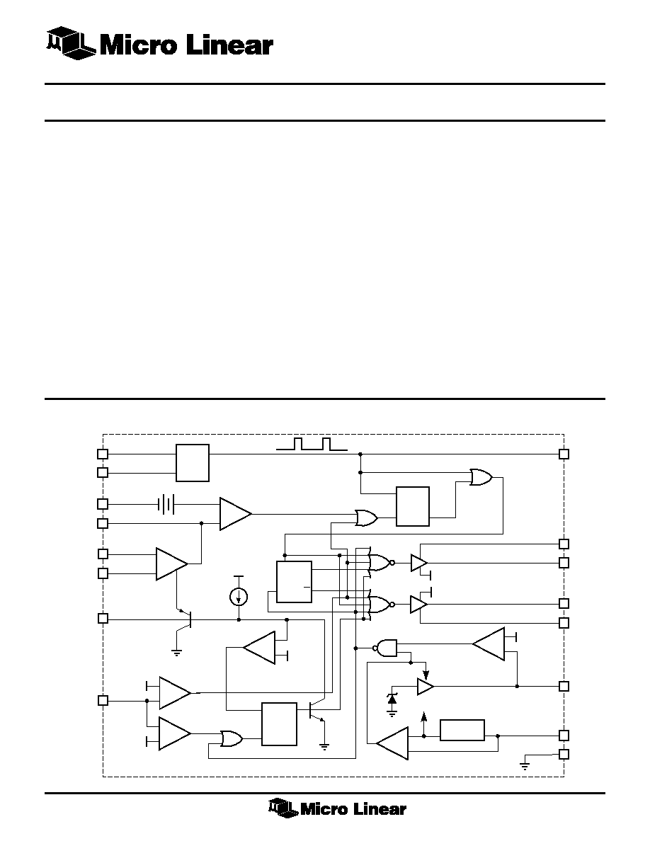
GENERAL DESCRIPTION
The ML4825 High Frequency PWM Controller is an IC
controller optimized for use in Switch Mode Power
Supply designs running at frequencies to 1MHz.
Propagation delays are minimal through the comparators
and logic for reliable high frequency operation while slew
rate and bandwidth are maximized on the error amplifier.
This controller is designed to work in either voltage or
current mode and provides for input voltage feed forward.
A 1V threshold current limit comparator provides cycle-
by-cycle current limit while exceeding a 1.4V threshold
initiates a soft-start cycle. The soft start pin doubles as a
maximum duty cycle clamp. An under-voltage lockout
circuit with 800mV of hysteresis assures low startup
current and drives the outputs low.
This controller is similar in architecture and performance
to the UC1825 controller, however the ML4825 includes
many features not found on the 1825. These features are
set in
Italics.
BLOCK DIAGRAM
(Pin configuration shown for 16-pin version)
*Some Packages Are Obsolete or End Of Life
+
+
≠
R
T
OUT A
E/A OUT
I
LIM
/SD
INV
SS
1.4V
1V
9
µ
A
V+
1V
R
POWER V
C
POWER GND
P
4V
R
TF.F.
OSC
S
UNDER
VOLTAGE
LOCKOUT
INTERNAL
BIAS
Q
ENABLE
V
REF
V
REF
GEN
9V
Q
Q
C
Q
S
RAMP
C
T
CLOCK OUT
PWR V
C
OUT B
PWR GND
V
CC
SIGNAL GND
NI
5
6
7
4
13
11
14
10
15
12
3
2
1
9
8
+
≠
+
≠
≠
+
≠
+
≠
+
+
≠
1.5V V
REF
16
COMP
ERROR
AMP
1.25V
FEATURES
s
Practical operation at switching frequencies to 1.0MHz
s
High current (2A peak) dual totem pole outputs
s
Wide bandwidth error amplifier
s
Fully latched logic with double pulse suppression
s
Pulse-by-pulse current limiting
s
Soft start and maximum duty cycle control
s
Under voltage lockout with hysteresis
s
Precision trimmed 5.1V bandgap reference
s
Pin compatible improved replacement for UC1825
s
Fast shut down path from current limit to outputs
s
Outputs preset to known condition after under voltage
lockout
s
Soft start latch ensures full soft start cycle
s
Outputs pull low for undervotage lockout
ML4825
2
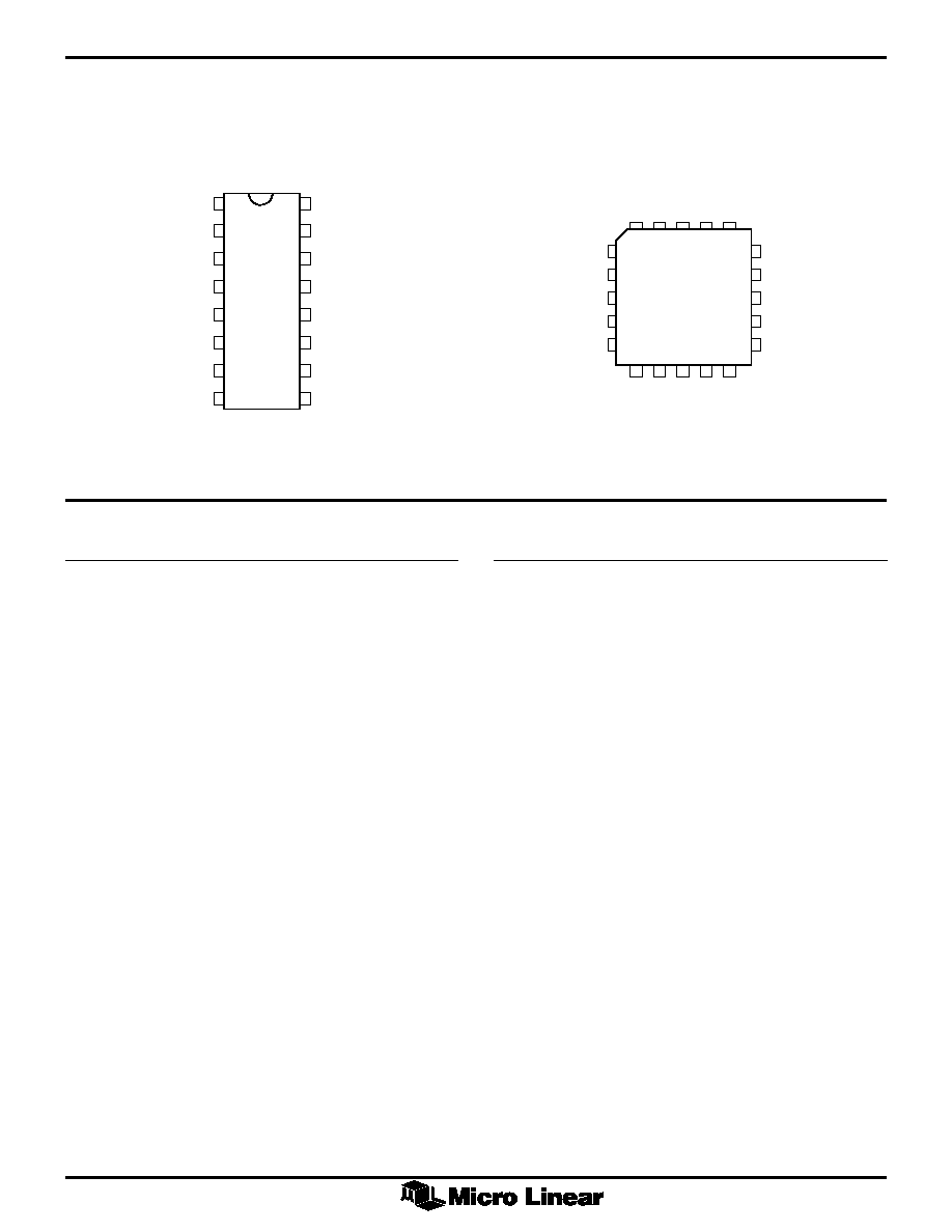
PIN CONFIGURATION
PIN
NAME
FUNCTION
PIN
NAME
FUNCTION
1 (2) INV
Inverting input to error amp.
2 (3) NI
Non-inverting input to error amp.
3 (4) E/A OUT
Output of error amplifier and input
to main comparator
4 (5) CLOCK
Oscillator output
5 (7) R
T
Timing resistor for oscillator--
sets charging current for oscillator
timing capacitor (pin 6)
6 (8) C
T
Timing capacitor for oscillator
7 (9) RAMP
Non-inverting input to main
comparator. Connected to C
T
for
voltage mode operation or to current
sense resistor for current mode
8 (10) SS
Normally connected to soft start
capacitor
9 (12) I
LIM
/SD
Current limit sense pin. Normally
connected to current sense resistor.
10 (13) GND
Analog signal ground
11 (14) OUT A
High current totem pole output. This
output is the first one energized after
power on reset
12 (15) PWR GND Return for the high current totem
pole outputs
13 (17) V
C
Positive supply for the high current
totem pole output
14 (18) OUT B
High current totem pole output
15 (19) V
CC
Positive supply for the IC
16 (20) 5.1V REF
Buffered output for the 5.1V voltage
reference
PIN DESCRIPTION
(Pin number in parentheses is for PLCC version)
ML4825
16-Pin PDIP
16-Pin SOIC
ML4825
20-Pin PLCC
INV
NI
E/A OUT
CLOCK
R
T
C
T
RAMP
SS
5.1V REF
V
CC
OUT B
V
C
PWR GND
OUT A
GND
I
LIM
/SD
1
2
3
4
5
6
7
8
16
15
14
13
12
11
10
9
TOP VIEW
OUT B
V
C
NC
PWR GND
OUT A
E/A OUT
CLOCK
NC
R
T
C
T
9
10 11
12
13
NI
INV
NC
5.1V REF
V
CC
RAMP
SS
NC
I
LIM
/SD
GND
4
5
6
7
8
3
2
1
20
19
18
17
16
15
14
TOP VIEW

ML4825
3
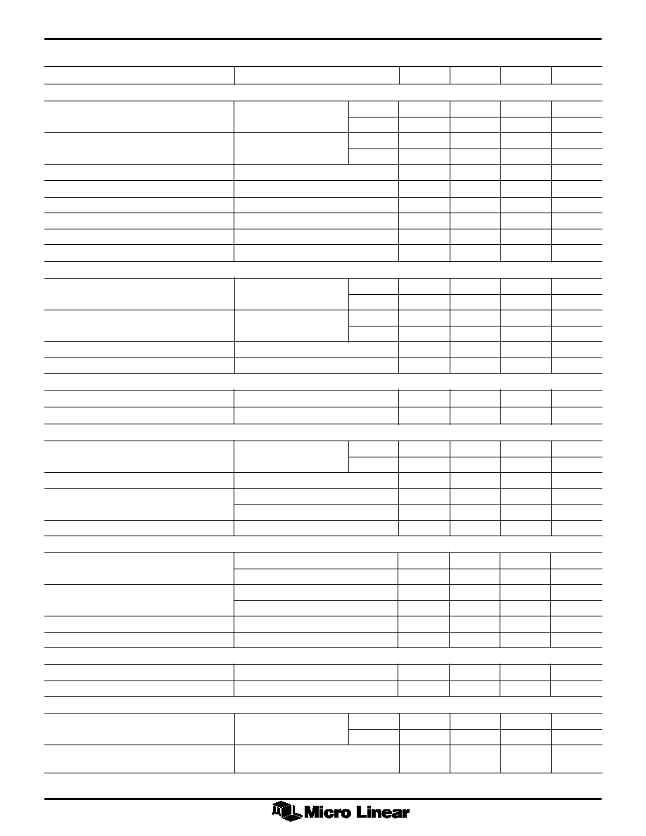
ELECTRICAL CHARACTERISTICS
Unless otherwise specified, R
T
= 3.65k
,
C
T
= 1000pF, T
A
= Operating Temperature Range, V
CC
= 15V (Note 1).
PARAMETER
CONDITIONS
MIN
TYP
MAX
UNITS
OSCILLATOR
Initial Accuracy
T
J
= 25
∞
C
360
400
440
kHz
Voltage Stability
10V < V
CC
< 30V, T
A
= 25
∞
C
≠2
0.2
2
%
Temperature Stability
5
%
Total Variation
Line, temperature
340
460
kHz
Clock Out High
3.9
4.5
V
Clock Out Low
2.3
2.9
V
Ramp Peak
2.6
2.8
3.0
V
Ramp Valley
0.7
1.0
1.25
V
Ramp Valley to Peak
1.6
1.8
2.0
V
REFERENCE
Output Voltage
T
J
= 25
∞
C, I
O
= 1mA
C suffix
5.00
5.10
5.20
V
I suffix
5.00
5.10
5.20
V
Line Regulation
10V < V
CC
< 30V
≠20
2
20
mV
Load Regulation
1mA < I
O
< 10mA
≠20
5
20
mV
Temperature Stability
≠55
∞
C < T
J
< 150
∞
C
0.2
0.4
%
Total Variation
Line, load, temperature
C suffix
4.95
5.25
V
I suffix
4.95
5.25
V
Output Noise Voltage
10Hz to 10kHz
50
µ
V
Long Term Stability
T
J
= 125
∞
C, 1000 hours
5
25
mV
Short Circuit Current
V
REF
= 0V
≠15
≠50
≠100
mA
ERROR AMPLIFIER
Input Offset Voltage
C suffix
≠15
15
mV
I suffix
≠15
15
mV
Input Bias Current
0.6
3
µ
A
Input Offset Current
0.1
1
µ
A
Open Loop Gain
1 < V
O
< 4V
60
96
dB
ABSOLUTE MAXIMUM RATINGS
Absolute maximum ratings are those values beyond which
the device could be permanently damaged. Absolute
maximum ratings are stress ratings only and functional
device operation is not implied.
Supply Voltage (V
C,
V
CC
) ........................................... 30V
Output Current, Source or Sink (OUT A, OUT B)
DC ....................................................................... 0.5A
Pulse (0.5
µ
s) ......................................................... 2.0A
Analog Inputs
(INV, NI, RAMP)................................ GND ≠0.3V to 7V
(SS, I
LIM
) ........................................... GND ≠0.3V to 6V
CLOCK Output Current ........................................... ≠5mA
E/A OUT Output Current .......................................... 5mA
Soft Start Sink Current ............................................ 20mA
R
T
Charging Current ................................................ ≠5mA
Junction Temperature
ML4825IX, ML4825CX ....................................... 150
∞
C
Storage Temperature Range ..................... ≠65
∞
C to 150
∞
C
Lead Temperature (soldering 10 sec.) ..................... 260
∞
C
Thermal Resistance (
JA
)
Plastic DIP or SOIC ......................................... 65
∞
C/W
Plastic Chip Carrier (PCC) ................................ 60
∞
C/W
OPERATING CONDITIONS
Temperature Range
ML4825CX ................................................ 0
∞
C to 70
∞
C
ML4825IX .............................................. ≠40
∞
C to 85
∞
C
ML4825
4
ELECTRICAL CHARACTERISTICS
(Continued)
PARAMETER
CONDITIONS
MIN
TYP
MAX
UNITS
ERROR AMPLIFIER (Continued)
CMRR
1.5V < V
CM
< 5.5V
C suffix
75
95
dB
I suffix
75
95
dB
PSRR
10V < V
CC
< 30V
C suffix
80
110
dB
I suffix
80
110
dB
Output Sink Current
V
EA OUT A
= 1.0V
1
2.5
mA
Output Source Current
V
EA OUT A
= 4.0V
≠0.5
≠1.3
mA
Output High Voltage
I
EA OUT A
= ≠0.5mA
4.0
4.7
5.0
V
Output Low Voltage
I
EA OUT A
= 1mA
0
0.5
1.0
V
Unity Gain Bandwidth
3
5.5
MHz
Slew Rate
6
12
V/
µ
s
PWM COMPARATOR
Ramp Bias Current
V
RAMP
= 0V, T
A
> 0
∞
C
C suffix
≠1
≠5
µ
A
I suffix
≠5
µ
A
Duty Cycle Range
C suffix
85
100
%
I suffix
80
100
%
E/A OUT Zero DC Threshold
V
RAMP
= 0V
1.1
1.25
1.7
V
Delay to Output
50
80
nS
SOFT START
Charge Current
SS = 0.5V
≠3
≠9
≠20
µ
A
Discharge Current
SS = 1V
1
mA
CURRENT LIMIT/SHUTDOWN
I
LIM
Bias Current
0V < V
I(LIM)
< 0.5V
C suffix
≠10
10
µ
A
I suffix
≠10
10
µ
A
Current Limit Threshold
0.9
1
1.1
V
Shutdown Threshold
T
A
> 0
∞
C
1.25
1.4
1.55
V
T
A
< 0
∞
C
1.25
1.4
1.60
V
Delay to Output
40
70
ns
OUTPUT
Output Low Level
I
OUT
= 20mA
0.25
0.4
V
I
OUT
= 200mA
1.2
2.2
V
Output High Level
I
OUT
= ≠20mA
13.0
13.5
V
I
OUT
= ≠200mA
12.0
13.0
V
Collector Leakage
V
C
= 30V
100
500
µ
A
Rise/Fall Time
C
L
= 1000pF
30
60
ns
UNDERVOLTAGE LOCKOUT
Start Threshold
8.8
9.2
9.6
V
UVLO Hysteresis
0.3
0.8
1.2
V
SUPPLY
Start Up Current
V
CC
= 8V
C suffix
0.1
1.1
2.5
mA
I suffix
0.1
3.5
mA
I
CC
V
INV,
V
RAMP,
V
I(LIM)/SD
= 0V,
10
26
33
mA
V
NI
= 1V, T
A
= 25
∞
C
Note 1: Limits are guaranteed by 100% testing, sampling, or correlation with worst-case test conditions.
ML4825
5
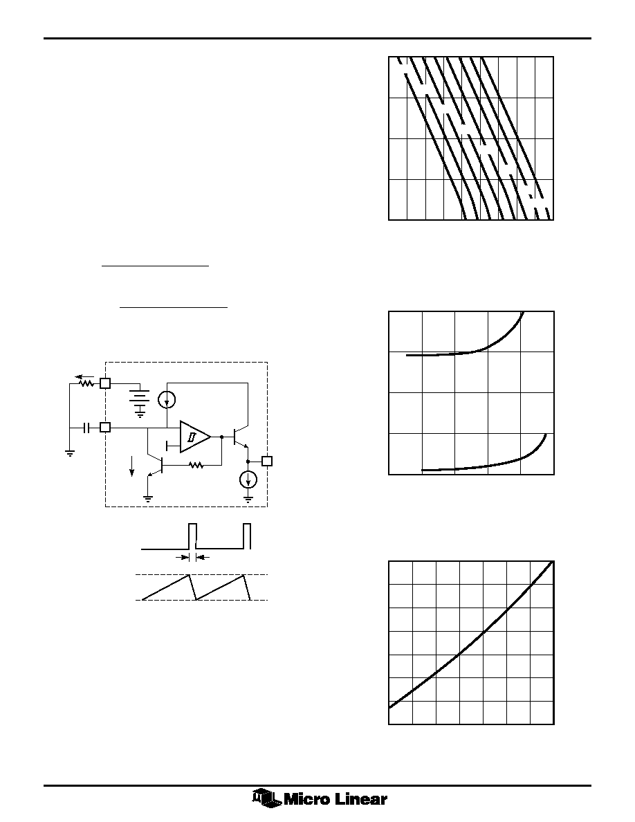
FUNCTIONAL DESCRIPTION
OSCILLATOR
The ML4825 oscillator charges the external capacitor (C
T
)
with a current (I
SET
) equal to 3/R
SET
. When the capacitor
voltage reaches the upper threshold (Ramp Peak), the
comparator changes state and the capacitor discharges to
the lower threshold (Ramp Valley) through Q1. While the
capacitor is discharging, Q2 provides a high pulse.
The oscillator period can be described by the following
relationship:
t
OSC
= t
RAMP
+ t
DEADTIME
where:
t
C Ramp Valley to Peak
I
RAMP
SET
=
(
)
and:
t
C Ramp Valley to Peak
I
DEADTIME
Q
=
(
)
1
Figure 1. Oscillator Block Diagram
I
SET
R
T
3V
C
T
I
SET
5.1V
Q1
I
Q1
CLOCK
t
D
RAMP PEAK
RAMP VALLEY
C
T
4
6
5
+
≠
100k
10k
1k
R
T
(
)
FREQUENCY (Hz)
100
1k
10k
1M
100k
100nF
47nF
22nF
0nF
4.7nF
2.2nF
1nF
470pF
160
140
120
100
80
T
D
(ns)
FREQUENCY (Hz)
10k
100k
1M
1.0nF
470pF
4.70
2.20
1.00
0.47
0.22
0.10
0.047
T
D
(
µ
s)
CT (nF)
0.47
2.2
100
22
1.0
4.7
47
10.0
Figure 2. Oscillator Timing Resistance vs Frequency
Figure 3. Oscillator Deadtime vs Frequency
Figure 4. Oscillator Deadtime vs C
T
(3k
R
T
100k
)