 | –≠–ª–µ–∫—Ç—Ä–æ–Ω–Ω—ã–π –∫–æ–º–ø–æ–Ω–µ–Ω—Ç: ML4835 | –°–∫–∞—á–∞—Ç—å:  PDF PDF  ZIP ZIP |

July 2000
PRELIMINARY
ML4835
*
Compact Fluorescent Electronic Dimming
Ballast Controller
1
GENERAL DESCRIPTION
The ML4835 is a complete solution for a dimmable or a
non-dimmable, high power factor, high efficiency
electronic ballast especially tailored for a compact
fluorescent lamp (CFL). The Bi-CMOS ML4835 contains
controllers for "boost" type power factor correction as
well as for a dimming ballast with end-of-lamp life
detection.
The PFC circuits uses a new , simple PFC topology which
requires only one loop for compensation. In addition,
this PFC can be used with either peak- or average-current
mode. This system produces a power factor of better than
0.99 with low input current THD.
The ballast controller section provides for programmable
starting sequence with individual adjustable preheat and
lamp out-of-socket interrupt times. The ML4835 provides
a shut down for both PFC and ballast controllers in the
event of end-of-life for the CFL.
BLOCK DIAGRAM
FEATURES
s
Power detect for end-of-lamp-life detection
s
Low distortion , high efficiency continuous boost, peak
or average current sensing PFC section
s
Leading- and trailing-edge synchronization between
PFC and ballast
s
One to one frequency operation between PFC and
ballast
s
Programmable start scenario for rapid/instant start lamps
s
Triple frequency control network for dimming or
starting to handle various lamp sizes
s
Programmable restart for lamp out condition to reduce
ballast heating.
s
Internal over-temperature shutdown
s
PFC over-voltage comparator eliminates output
"runaway" due to load removal
s
Low start-up current; < 0.55mA
7
RSET
9
RT/CT
8
RT2
13
CRAMP
4
PIFBO
3
PIFB
2
PEAO
1
PVFB/OVP
12
PWDET
10
INTERRUPT
5
LAMP FB
6
LEAO
17
OUT A
16
OUT B
18
PFC OUT
15
PGND
11
RX/CX
19
VCC
20
REF
14
AGND
OUTPUT
DRIVERS
PRE-HEAT AND
INTERRUPT TIMERS
LAMP OUT DETECT
AND
AUTOMATIC LAMP
RESTART
UNDER-VOLTAGE
AND
THERMAL SHUTDOWN
END-OF-LAMP DETECT
AND
POWER SHUTOFF
ANTI-FLASH
COMPENSATION
AND
POWER DIMMING LEVEL
INTERFACE
CONTROL
AND
GATING
LOGIC
THREE-FREQUENCY
CONTROL SEQUENCER
VCO
VARIABLE FREQUENCY
OSCILLATOR
POWER
FACTOR
CONTROLLER
(* Indicates Part is End Of Life as of July 1, 2000)

ML4835
2
PIN CONFIGURATION
PIN DESCRIPTION
PIN
NAME
FUNCTION
1
PVFB/OVP
Inverting input to the PFC error
amplifier and OVP comparator input.
2
PEAO
PFC error amplifier output and
compensation node
3
PIFB
Senses the inductor current and peak
current sense point of the PFC cycle
by cycle current limit
4
PIFBO
Output of the current sense amplifier.
Placing a capacitor to ground will
average the inductor current.
5
LAMP FB
Inverting input of the lamp error
amplifier, used to sense and regulate
lamp arc current. Also the input node
for dimmable control.
6
LEAO
Output of the lamp current error
transconductance amplifier used for
lamp current loop compensation
7
R
SET
External resistor which SETS oscillator
F
MAX
, and R
X
/C
X
charging current
8
R
T2
Oscillator timing component to set
start frequency
9
R
T
/C
T
Oscillator timing components
PIN
NAME
FUNCTION
10
INTERRUPT Input used for lamp-out detection and
restart. A voltage less than 1V will
reset the IC and cause a restart after a
programmable interval.
11
R
X
/C
X
Sets the timing for preheat and
interrupt.
12
PWDET
Lamp output power detection
13
C
RAMP
Integrated voltage of the error
amplifier out
14
AGND
Analog ground
15
PGND
Power ground.
16
OUT B
Ballast MOSFET driver output
17
OUT A
Ballast MOSFET driver output
18
PFC OUT
Power factor MOSFET driver output
19
V
CC
Positive supply voltage
20
REF
Buffered output for the 7.5V reference
1
2
3
4
5
6
7
8
9
10
20
19
18
17
16
15
14
13
12
11
ML4835
20-Pin SOIC (S20)
20-Pin DIP (P20)
PVFB/OVP
PEAO
PIFB
PIFBO
LAMP FB
LEAO
RSET
RT2
RT/CT
INTERRUPT
REF
VCC
PFC OUT
OUT A
OUT B
PGND
AGND
CRAMP
PWDET
RX/CX

ML4835
3
ABSOLUTE MAXIMUM RATINGS
Absolute maximum ratings are those values beyond which
the device could be permanently damaged. Absolute
maximum ratings are stress ratings only and functional
device operation is not implied.
Supply Current (I
CC) .............................................................
65mA
Output Current, Source or Sink
(OUT A, OUT B, PFC OUT) DC ........................... 250mA
PIFB Input Voltage ............................................≠3V to 2V
Maximum Forced Voltage
(PEAO, LEAO) ............................................ ≠0.3V to 7.7V
Maximum Forced Current
(PEAO, LEAO) ...................................................... ±20mA
Junction Temperature .............................................. 150∫C
Storage Temperature Range ...................... ≠65∫C to 150∫C
Lead Temperature (Soldering, 10 sec) ..................... 260∫C
Thermal Resistance (
q
JA
)
ML4835CP .......................................................... 65∫C/W
ML4835CS .......................................................... 80∫C/W
OPERATING CONDITIONS
Temperature Range ....................................... 0∞C to 85∞C
ELECTRICAL CHARACTERISTICS
Unless otherwise specified, V
CC
= V
CCZ
≠0.5V, R
SET
= 11.8k
W, R
T
= 15.4k
W, R
T2
= 67.5k
W, C
T
= 1.5nF,
T
A
= Operating Temperature Range (Note 1)
SYMBOL
PARAMETER
CONDITIONS
MIN
TYP
MAX
UNITS
LAMP CURRENT AMPLIFIER (LAMP FB, LEAO)
Input Bias Current
-0.3
-1.0
µA
Small Signal Transconductance
35
75
105
µ
W
Input Bias Voltage
-0.3
5.0
V
Output Low
LAMP FB = 3V, R
L
=
•
0.2
0.4
V
Output High
LAMP FB = 2V, R
L
=
•
7.1
7.5
V
Source Current
LAMP FB = 0V, LEAO = 6V
-80
-220
µA
Sink Current
LAMP FB = 5V, LEAO = 0.3V
80
220
µA
PFC VOLTAGE FEEDBACK AMPLIFIER ( PEAO, PVFB/OVP)
Input Bias Current
-0.3
-1.0
µA
Small Signal Transconductance
35
75
105
µ
W
Input Bias Voltage
-0.3
5.0
V
Output Low
PVFB = 3V, R
L
=
•
0.2
0.4
V
Output High
PVFB = 2V, R
L
=
•
6.4
6.8
V
Source Current
PVFB = 0V, PEAO = 6V
-80
220
µA
Sink Current
PVFB = 5V, PEAO = 0.3V
80
220
µA
PFC CURRENT-LIMIT COMPARATOR (PIFB)
Current-Limit Threshold
-0.9
-1.0
-1.1
V
Propagation Delay
100mV Step and 100mV Overdrive
100
ns
PFC OVP COMPARATOR
OVP Threshold
2.65
2.75
2.85
V
Hysteresis
0.14
0.20
0.30
V
Propagation Delay
1.4
µs

ML4835
4
ELECTRICAL CHARACTERISTICS
(Continued)
SYMBOL
PARAMETER
CONDITIONS
MIN
TYP
MAX
UNITS
OSCILLATOR
Initial Accuracy (F
MIN
)
T
A
= 25∫C
39.2
40
40.8
kHz
Voltage Stability (F
MIN
)
V
CCZ
≠ 4V < V
CC
< V
CCZ
≠ 0.5V
0.3
%
Temperature Stability (F
MIN
)
0.3
%
Total Variation (F
MIN
)
Line, Temperature
39.2
40.8
kHz
Initial Accuracy (START)
T
A
= 25∫C
49
50
51
kHz
Voltage Stability (START)
0.3
%
Temparature Stability (START)
0.3
%
Total Variation (START)
Line, Temperature
49
51
kHz
Ramp Valley to Peak
2.5
V
Initial Accuracy (Preheat)
TA = 25∫C
60.8
64
67.2
kHz
Total Variation (Preheat)
Line, Temperature
60.8
64
67.2
kHz
C
T
Discharge Current
V
RTCT
= 2.5V
6.0
7.5
9.0
mA
Output Drive Deadtime
C
T
= 1.5nF
0.7
us
REFERENCE BUFFER
Output Voltage
T
A
= 25∫C, I
O
= 0mA
7.4
7.5
7.6
V
Line Regulation
V
CCZ
≠ 4V < V
CC
< V
CCZ
≠ 0.5V
10
25
mV
Load Regulation
1mA < I
O
< 10mA
2
15
mV
Temperature Stability
0.4
%
Total Variation
Line, Load, Temperature
7.35
7.65
V
Long Term Stabilty
Tj=125∫C, 1000 hrs
5
mV
Short Circuit Current
40
mA
R
SET
Voltage
2.4
2.5
2.6
V

ML4835
5
ELECTRICAL CHARACTERISTICS
(Continued)
SYMBOL
PARAMETER
CONDITIONS
MIN
TYP
MAX
UNITS
PREHEAT AND INTERRUPT TIMER (R
X
= 346k
W, C
X
= 10µF)
Initial Preheat Period
0.86
s
Subsequenct Preheat Period
0.72
s
Interrupt Period
5.9
s
R
X
/C
X
Charging Current
-50
-54
-58
µA
R
X
/C
X
Open Circuit Voltage
0.4
0.7
1.0
V
R
X
/C
X
Maximum Voltage
7.0
7.3
7.8
V
Preheat Lower Threshold
1.6
1.75
1.9
V
Preheat Upper Threshold
4.4
4.65
4.9
V
Start Period End Threshold
6.2
6.6
6.9
V
Interrupt Disable Threshold
1.1
1.25
1.4
V
Hysteresis
0.16
0.26
0.36
V
Input Bias Current
1
µA
POWER SHUTDOWN
Power Shutdown Voltage
0.9
1
1.1
V
OUTPUTS (OUT A, OUT B, PFC OUT)
Output Voltage Low
I
OUT
= 20mA
0.1
0.2
V
I
OUT
= 200mA
1.0
2.0
V
Output Voltage High
I
OUT
= 20mA
V
CC
-0.2
V
CC
-0.1
V
Output Voltage High
I
OUT
= 200mA
V
CC
-2.0
V
CC
-1.0
V
Output Voltage Low in UVLO
I
OUT
= 10mA, V
CC
< V
CC START
0.2
V
Output Rise and Fall Time
CL=1000pF
50
ns
UNDER VOLTAGE LOCKOUT AND BIAS CIRCUITS
IC Shunt Voltage (V
CCZ
)
ICC=15mA
14.0
14.8
15.5
V
Start-up Threshold (V
CC START
)
V
CCZ
-1.5 V
CCZ
-1.0 V
CCZ
-0.5
V
Hysteresis
3.0
3.7
4.4
V
Start-up Current
V
CC START
≠0.2V
350
550
µA
Interrupt Current
(V
CC
≠0.5V), INTERRUPT = 0V
500
750
µA
Operating Current
(V
CC
≠0.5V)
5.5
8.0
mA
Shutdown Temperature
130
∫C
Hysteresis
30
∫C
Note 1:
Limits are guaranteed by 100% testing, sampling, or correlation with worst case test conditions.

ML4835
6
FUNCTIONAL DESCRIPTION
The ML4835 consists of peak or average current
controlled continuous boost power factor front end section
with a flexible ballast control section. Start-up and lamp-
out retry timing are controlled by the selection of external
timing components, allowing for control of a wide variety
of different lamp types. The ballast section controls the
lamp power using frequency modulation (FM) with
additional programmability provided to adjust the VCO
frequency range. This allows for the IC to be used with a
variety of different output networks. Figure 1 depicts a
detailed block diagram of ML4835.
The ML4835 provides several safety features. See the
corresponding sections for more details:
∑ End-of-lamp life detection to detect EOL and shut-off
lamps; See End Of Life Section.
∑ Thermal shutdown for temperature sensing extremes;
See IC Bias, Under-Voltage Lockout and Thermal
Shutdown Section.
∑ Relamping starting with anti-flash for programmable
restart for lamp out conditions while minimizing
"flashing" when powering from full power to dimming
levels; See Starting, Re-Start, Preheat and Interrupt
Section
Figure 1. Detailed Block Diagram
VCC
19
REF
20
AGND
14
CRAMP
13
PVFB/OVP
1
PEAO
2
PIFB
PIFBO
4
PFC OUT
18
RSET
7
LAMP FB
5
LEAO
6
RT2
8
INTERRUPT
10
PWDET
12
PGND
15
OUT B
16
OUT A
17
REF
≠
+
14V
+
≠
6.75V
Q
Q
R
S
Q
Q
T
+
≠
TEMP
130∫C/100∫C
+
≠
1.25V/1V
RX/CX
6.75V/1.25V
2.5V
+
≠
1.0V
Q
Q
S
R
≠
+
≠
+
+
≠
4.75V/
1.75V
+
≠
PVFB
2.75V
+
≠
≠1V
+
≠
3
R
S
Q
Q
R
S
Q
Q
≠
+
2.5V
V
TO
I
˜2
CLK1
CLK
RX/CX
11
PFC CONTROLLER
OVP
ILIM
UVLO
REF_OK
PREHEAT
THERMAL SHUTDOWN
RT/CT
9
OSCILLATOR
V
TO
I
V
TO
I
COMP

ML4835
7
Figure 3. ML4835 PFC Controller Section
FUNCTIONAL DESCRIPTION
(Continued)
The ML4835 implements a triple frequency operation
scheme: programmable three-frequency sequence for pre-
heat, ignition, and dimming, that extends lamp life,
simplifies lamp network design, and starts lamps at any
dimming level without flashing. This addresses the need
for a high-Q network for starting sequence and low-Q
network for operation, minimizing parasitic losses and
improving overall power efficiency. The values for the
pre-heat, start, operation, and restart can be programmed
or selected (Figure 2).
POWER FACTOR SECTION
The ML4835 power factor section is a peak or average
current sensing boost mode PFC control circuit in which
only voltage loop compensation is needed. It is simpler
than a conventional average current control method. It
consists of a voltage error amplifier, a current sense
amplifier (no compensation is needed), an integrator, a
comparator, and a logic control block. In the boost
topology, power factor correction is achieved by sensing
the output voltage and the current flowing through the
current sense resistor. Duty cycle control is achieved by
comparing the integrated voltage signal of the error
amplifier and the voltage across R
SENSE
. The duty cycle
control timing is shown in Figure 3.
+
≠
≠
+
LAMP
NETWORK
INVERTER
LAMP
LAMP
RA
SW2
L
SW1
R
SENSE
RB
V
OUT
EMI
FILTER
18
3
PIFB
PIFBO
C
RAMP
C1
C2
R1
C
RAMP
PFC OUT
PVFB/OVP
1
≠A
S
VREF1
OSC
PIFBO
RAMP
CLK
PFC OUT
CLK
R
Q
V
TO
I
PEAO
13
PEAO
2
4
START
HIGH Q
LOW Q
OPERATION
PREHEAT
f3
f2
f1
ML4835
SET TIME VALUES
FOR PREHEAT,
START AND OPERATION,
AND RESTART
Figure 2. Three Frequency Design Model
ML4835
8
Setting minimum input voltage for output regulation can
be achieved by selecting C
RAMP
as follows for peak
current mode:
C
PEAO
K
D Ts
t
P
V
V
V
L
D Ts
R
RAMP
MAX
OUT
IN
OUT
IN
SENSE
=
-
-
-
-
-
!
"
$
#
#
¥
22
1
1
2
2
2
1
8
(
)
(
)
D
:
?
(1)
And for average current mode:
C
PEAO
K
D Ts
t
P
V
V
L
D Ts
R
RAMP
MAX
OUT
IN
OUT
SENSE
=
-
-
-
-
!
"
$
#
#
¥
22
1
1
2
2
1
8
(
)
(
)
D
:
?
(1a)
Where
Dt is the dead time.
OVERVOLTAGE PROTECTION AND INHIBIT
The OVP pin serves to protect the power circuit from
being subjected to excessive voltages if the load should
change suddenly (lamp removal). A divider from the high
voltage DC bus sets the OVP trip level. When the voltage
on PVFB/OVP exceeds 2.75V, the PFC transistor are
inhibited. The ballast section will continue to operate.
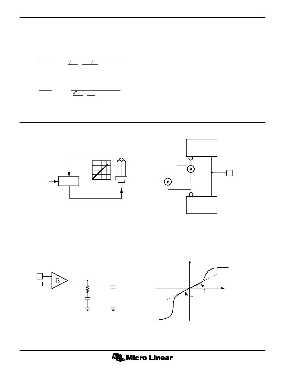
TRANSCONDUCTANCE AMPLIFIERS
The PFC voltage feedback amplifier is implemented as an
operational transconductance amplifier. It is designed to
have low small signal forward transconductance such that
a large value of load resistor (R1) and a low value
ceramic capacitor (<1µF) can be used for AC coupling
FUNCTIONAL DESCRIPTION
(Continued)
Figure 5. Compensation Network
Figure 6. Output Configuration
Figure 7. Transconductance Amplifier Characteristics
≠
+
1
2.5V
PVFB/OVP
R1
C1
C2
CURRENT
MIRROR
IN
OUT
CURRENT
MIRROR
IN
OUT
gmV
IN
io = gmV
IN
IQ +
2
gmV
IN
IQ ≠
2
V
IN
DIFFERENTIAL
LINEAR SLOPE REGION
0
i
O
Figure 4. Simplified Model of ML4835 EOL Functionality
ML4835
POWER LEVEL
TRIP POINT
POWER DETECT
POWER SHUTOFF

ML4835
9
CLOCK
C
T
V
TH
= 3.75V
V
TL
= 1.25V
t
DIS
t
CHG
INTERRUPT
R
X
/C
X
10
11
3.75/1.25V
+
≠
1.25/1.0V
0.625
R
SET
V
CC
R
T2
REF
LEA_ENB
C
T
9
R
T2
R
T
≠
+
8
20
+
R
T
/C
T
5.5mA
I
CHG
DURING PREHEAT
AFTER PREHEAT
LEA_ENB = HI
LEA_ENB = LOW
I
RSET
CHG =
2.5V
I
RSET
CHG =
5V
8K±25%
≠
7.5V
I
RSET
CHG =
5V
8K±25%
≠ LEAO
NOTE 1: R
SET
SHOULD BE SELECTED SUCH THAT AFTER PREHEAT WITH LEA_ENB "HI",
I
CHG
MUST BE < 0.
I
CHG
IS A UNI-DIRECTIONAL SOURCE CURRENT ONLY.
19
4.75/1.25V
≠
+
7.5V
Figure 8. Oscillator Block Diagram and Timing
Figure 9. Typical V
CC
and I
CC
Waveforms when the ML4835 is Started with a Bleed Resistor from
the Rectified AC Line and Bootstrapped from an Auxiliary Winding.
VCCZ
V(ON)
V(OFF)
5.5mA
0.34mA
V
CC
I
CC
t
t

ML4835
10
(C1) in the frequency compensation network. The
compensation network shown in Figure 5 will introduce a
zero and a pole at:
f
R C
f
R C
Z
P
=
=
1
2
1
2
1 1
1 2
p
p
(2)
Figure 4 shows the output configuration for the
operational transconductance amplifiers.
A DC path to ground or V
CC
at the output of the
transconductance amplifiers will introduce an offset error.
The magnitude of the offset voltage that will appear at the
input is given by V
OS
= io/gm. For an io of 1µA and a gm
of 0.05 µW the input referred offset will be 20mV.
Capacitor C1 as shown in Figure 5 is used to block the
DC current to minimize the adverse effect of offsets.
Slew rate enhancement is incorporated into all of the
operational transconductance amplifiers in the ML4835.
This improves the recovery of the circuit in response to
power up and transient conditions. The response to large
signals will be somewhat non-linear as the
transconductance amplifiers change from their low to
high transconductance mode, as illustrated in Figure 7.
END OF LAMP LIFE
At the end of a lamp's life when the emissive material is
depleted, the arc current is rectified and high voltage
occurs across the lamp near the depleted cathode. The
ballast acts as a constant current source so power is
dissipated near the depleted cathode which can lead to
arcing and bulb cracking. Compact fluorescent lamps are
more prone to cracking or shattering because their small
diameter can't dissipate as much heat as the larger linear
lamps. Compact fluorescents also present more of a
safety hazard since they are usually used in downlighting
systems without reflector covers.
EOL and the ML4835
The ML4835 uses a circuit that creates a DC voltage
representative of the power supplied to the lamps through
the inverter. This voltage is used by the ML4835 to latch
off the ballast when it exceeds an internal threshold. An
external resistor can be used as the "EOL latch resistor" to
set the power level trip point, as shown in by R9 in Figure
12. See Micro Linear ML4835 User Guide and
applications notes for more details. Figure 4 illustrates a
simplified model of ML4835 EOL functionality.
BALLAST OUTPUT SECTION
The IC controls output power to the lamps via frequency
modulation with non-overlapping conduction. This means
that both ballast output drivers will be low during the
discharging time t
DIS
of the oscillator capacitor C
T
.
OSCILLATOR
The VCO frequency ranges are controlled by the output
of the LFB amplifier (R
SET
). As lamp current decreases,
LFB OUT falls in voltage, causing the C
T
charging current
to increase, thereby causing the oscillator frequency to
increase. Since the ballast output network attenuates high
frequencies, the power to the lamp will be decreased. The
oscillator frequency is determined by the following
equations:
F
t
t
OSC
CHG
DIS
=
+
1
(3)
and
t
R C In
V
I
R
V
V
II
R
V
CHG
T
T
REF
CHG
T
TL
REF
CHG
T
TH
=
+
¥
-
+
¥
-
(4)
The oscillator's minimum frequency is set when I
CHG
= 0
where:
F
R C
MIN
T
T
@
¥
1
0 51
.
(5)
The oscillator's start frequency can be expressed by:
F
R R
C
START
T
T
T
=
¥
¥
1
0 51
2
.
2
7
(5a)
Both equations assume that t
CHG
>> t
DIS
.
When LFB OUT is high, I
CHG
= 0 and the minimum
frequency occurs. The charging current varies according
to two control inputs to the oscillator:
1. The output of the preheat timer
2. The voltage at LFB OUT (lamp feedback amplifier
output)
In preheat condition, charging current is fixed at
I
R
CHG PREHEAT
SET
(
)
.
=
25
(6)
In running mode, charging current decreases as the
voltage rises from 0V to V
OH
at the LAMP FB amplifier.
The charging current behavior can be expressed as:
I
V
R
LEAO
k
CHG
SET
=
-
±
5
8
25%
(7)
The highest frequency is attained when I
CHG
is highest,
which is attained when voltage at LFB OUT is at 0V:
I
R
CHG
SET
( )
0
5
=
(8)
FUNCTIONAL DESCRIPTION
(Continued)

ML4835
11
Highest lamp power, and lowest output frequency are
attained when voltage at LFB OUT is at its maximum
output voltage (V
OH
).
In this condition, the minimum operating frequency of the
ballast is set per equation 5 above.
For the IC to be used effectively in dimming ballasts with
higher Q output networks a larger C
T
value and lower R
T
value can be used, to yield a smaller frequency excursion
over the control range (voltage at LFB OUT). The
discharge current is set to 5.5mA.
Assuming that I
DIS
>>I
RT
:
t
C
DIS VCO
T
(
)
@
¥
600
(9)
IC BIAS, UNDER-VOLTAGE LOCKOUT AND
THERMAL SHUTDOWN
The IC includes a shunt clamp which will limit the
voltage at V
CC
to 15V (V
CCZ
). The IC should be fed with
a current limited source, typically derived from the
ballast transformer auxiliary winding. When V
CC
is below
V
CCZ
≠ 1.1V, the IC draws less than 0.55mA of quiescent
current and the outputs are off. This allows the IC to start
using a "bleed resistor" from the rectified AC line.
To help reduce ballast cost, the ML4835 includes a
temperature sensor which will inhibit ballast operation if
the IC's junction temperature exceeds 130∞C. In order to
use this sensor in lieu of an external sensor, care should
be taken when placing the IC to ensure that it is sensing
temperature at the physically appropriate point in the
ballast. The ML4835's die temperature can be estimated
with the following equation:
T
T
P
C W
J
A
D
@
+
+ ∞
(
/
)
65
(10)
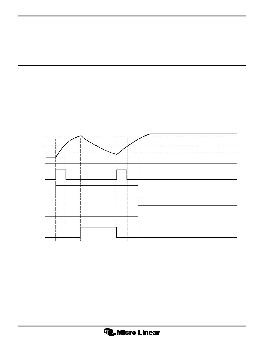
STARTING, RE-START, PREHEAT AND INTERRUPT
The lamp starting scenario implemented in the ML4835
is designed to maximize lamp life and minimize ballast
heating during lamp out conditions.
The circuit in Figure 10 controls the lamp starting
scenarios: Filament preheat and lamp out interrupt. C
X
is
charged with a current of I
R(SET)
/4 and discharged through
R
X
. The voltage at C
X
is initialized to 0.7V (V
BE
) at power
up. The time for C
X
to rise to 4.75V is the filament preheat
time. During that time, the oscillator charging current
(I
CHG
) is 2.5/R
SET
. This will produce a high frequency for
filament preheat, but will not produce sufficient voltage
to ignite the lamp or cause significant glow current.
After cathode heating, the inverter frequency drops to
F
START
causing a high voltage to appear to ignite the
lamp. If lamp current is not detected when the lamp is
supposed to have ignited, the C
X
charging current is shut
off and the inverter is inhibited until C
X
is discharged by
R
X
to the 1.25V threshold. Shutting off the inverter in this
manner prevents the inverter from generating excessive
heat when the lamp fails to strike or is out of socket.
Typically this time is set to be fairly long by choosing a
large value of R
X
.
LFB OUT is ignored by the oscillator until INTERRUPT is
above 1.25V The C
X
pin is clamped to about 7.5V.
Care should also be taken not to turn on the VCCZ clamp
so as not to dissipate excessive power in the IC. This will
cause the temp sensor to become active at a lower
ambient temperature.
A summary of the operating frequencies in the various
operating modes is shown below.
OPERATING MODE
OPERATING FREQUENCY
[F(MAX) to F(MIN)]
Preheat
2
After
Preheat
F(START)
Dimming
Control
F(MIN) to F(MAX)
Figure 10. Lamp Preheat and Interrupt Timers
FUNCTIONAL DESCRIPTION
(Continued)
R
X
C
X
HEAT
INHIBIT
0.625
R
SET
LEA_ENB OR
DIMMING LOCKOUT
INTERRUPT
10
R
X
/C
X
S
R
Q
1.25/4.75
+
≠
1.0/1.25
+
≠
1.25/6.75
+
≠
9
ML4835
12
Figure11. Lamp Starting and Restart Timing
6.75
7.5
4.75
1.25
.7
0
R
X
/C
X
HEAT
LEA_ENB OR
DIMMING LOCKOUT
INTERRUPT
INHIBIT
TYPICAL APPLICATIONS
The ML4835 can be used for a variety of lamp types:
T4 or compact fluorescent lamps
IEC T8 (linear lamps)
T5 linear lamps
T12 linear lamps
The ML4835 can also be used for dimming applications.
For example, 20:1 dimming can be achieved using the
ML4835 with external dimming units. The applications
schematics shown in Figures 12, 13, and 14 are examples
of the various uses of the ML4835.

ML4835
13
Figure12. Ballast for Architectural Dimming Applications
U1
F1
L1
L2
C1
3.3nF
C2
3.3nF
C6
0.1µF
C3
0.15µF
D1
D2
D3
D5
1A, 50V
D6
1A, 50V
D4
D9, 0.1A
75V
D18
0.1A
75V
D14
0.1A
75V
D11, 15V, 0.5W
D13
5.6V, 0.5W
120VRMS
R4, 62k
D10, 0.1A
75V
D7
1A, 600V
(ULTRA-
FAST)
D8, 1A, 600V
R25
100
R7
432k
R6
432k
T1
6
10
8
9
Q1
4.5A, 500V
R8
5.76k
R9
4.3
R24
20k
C8
47µF
HOT
NEUTRAL
R
Y
B
R
Y
B
C30
120pF
C28
120pF
C14
0.015µF
D19
1A
600V
D15
1A
600V
D12
0.1A, 75V
C12
0.33µF
4
3
2
1
8
9
5
1
6
10
T3
D16, 0.1A, 75V
R11
150
R10
30
C9
1µF
Q2
2.5A, 500V
6
7
D17, 0.1A, 75V
R12
150
1
8
Q3
2.5A, 500V
T3
1
2
3
4
5
6
7
8
9
10
20
19
18
17
16
15
14
13
12
11
R13
1k
C15
1µF
R14
22.6k
PVFB
PEAO
PIFB
PIFBO
LFB
LEAO
RSET
RT2
RT/CT
INTRPT
REF
VCC
PFC OUT
OUT A
OUT B
P GND
A GND
RAMP
PW DET
RX/CX
ML4835
C29
100pF
C17
8.2nF
C16
82nF
C4
33nF
C18
1.5nF
R15, 681k
R17
4.3k
R22
360k
R18
8.06k
R26
5k
C19
1µF
C20
1.5nF
C22
1.5µF
C24
470pF
C25
0.22µF
C27
0.22µF
C1
100µF
C21
15µF
R23, 200k
R16
10k
C23
6.8µF
C26
47µF
+
≠
+
≠
VIOLET
GREY
MANUAL DIMMER
0-10VDC
T1
D2
18V
C4
10µF
R7
3.32k
R6
3.32k
Q1
D3
C2
220pF
R5
1M
C3, 1nF
R3
16.2k
R4
220k
U2A
U2B
R2
1.5k
U1
R1
604
C5
0.01µF
R8
180
D1
0.1A, 75V
3
4
1
2
3
4
5
6
7
8
1
2
5
4
DIMMER INTERFACE ASSEMBLY
D1-D4: 1A, 600V
R1
0.33
R2
100
R3
820
R19, 16.2k
R21, 51.1k
C5
0.1µF
C7
100µF
3
2
7
6
C11
6800pF

ML4835
14
Figure13. Ballast for Architectural Downlighting Applications
U1
F1
L1
L2
C1
3.3nF
C2
3.3nF
C6
0.1µF
C3
0.15µF
D1
D2
D3
D5
1A, 50V
D6
1A, 50V
D4
D9, 0.1A
75V
D18
0.1A
75V
D14
0.1A
75V
D11, 15V, 0.5W
D13
5.6V, 0.5W
120VRMS
R4, 62k
D10, 0.1A
75V
D7
1A, 600V
(ULTRA-
FAST)
D8, 1A, 600V
R25
100
R7
432k
R6
432k
T1
6
10
8
9
Q1
4.5A, 500V
R8
5.76k
C8
47µF
HOT
NEUTRAL
R
Y
B
R
Y
B
C30
120pF
C28
120pF
C10
0.33µF
C11
6800pF
C14
0.015µF
D19
1A
600V
D15
1A
600V
D12
0.1A, 75V
C13
2700pF
C12
0.33µF
4
3
2
1
8
9
5
1
6
10
7
6
10
T3
8
6
D16, 0.1A, 75V
R11
150
R10
30
C9
1µF
Q2
2.5A, 500V
3
2
6
7
D17, 0.1A, 75V
R12
150
1
8
Q3
2.5A, 500V
T3
1
2
3
4
5
6
7
8
9
10
20
19
18
17
16
15
14
13
12
11
R13
1k
C15
1µF
R14
22.6k
PVFB
PEAO
PIFB
PIFBO
LFB
LEAO
RSET
RT2
RT/CT
INTRPT
REF
VCC
PFC OUT
OUT A
OUT B
P GND
A GND
RAMP
PW DET
RX/CX
ML4835
C29
100pF
C17
8.2nF
C16
82nF
C4
33nF
C18
1.5nF
R15, 681k
R17
4.3k
R22
360k
R18
8.06k
R26
5k
C19
1µF
C20
1.5nF
C22
1.5µF
C24
470pF
C25
0.22µF
C27
0.22µF
C1
100µF
C21
15µF
R23, 200k
R16
10k
C23
6.8µF
C26
47µF
+
≠
+
≠
VIOLET
GREY
MANUAL DIMMER
0-10VDC
T1
D2
18V
C4
10µF
R7
3.32k
R6
3.32k
Q1
D3
C2
220pF
R5
1M
C3, 1nF
R3
16.2k
R4
220k
U2A
U2B
R2
1.5k
U1
R1
604
C5
0.01µF
R8
180
D1
0.1A, 75V
3
4
1
2
3
4
5
6
7
8
1
2
5
4
DIMMER INTERFACE ASSEMBLY
D1-D4: 1A, 600V
R1
0.33
R2
100
R3
820
C5
0.1µF
C7
100µF
R19, 16.2k
R21, 51.1k
R9
4.3
R24
20k
L3

ML4835
15
Figure14. Non-Dimming Ballast for Downlighting Applications
U1
F1
L1
L2
C1
3.3nF
C2
3.3nF
C6
0.1µF
C3
0.15µF
D1
D2
D3
D5
1A, 50V
D6
1A, 50V
D4
D9, 0.1A
75V
D18
0.1A
75V
D14
0.1A
75V
D11, 15V, 0.5W
120VRMS
R4, 62k
D10, 0.1A
75V
D7
1A, 600V
D8, 1A, 600V
R25
100
R7
432k
R6
432k
T1
6
10
8
9
Q1
4.5A, 500V
R8
5.76k
C8
47µF
HOT
NEUTRAL
R
Y
B
R
Y
B
C30
120pF
C28
120pF
C14
0.015µF
D19
1A
600V
D15
1A
600V
D12
0.1A, 75V
C12
0.33µF
4
3
2
1
8
9
5
1
6
10
T3
D16, 0.1A, 75V
R11
150
R10
30
C9
1µF
Q2
2.5A, 500V
6
7
D17, 0.1A, 75V
R12
150
1
8
Q3
2.5A, 500V
1
2
3
4
5
6
7
8
9
10
20
19
18
17
16
15
14
13
12
11
PVFB
PEAO
PIFB
PIFBO
LFB
LEAO
RSET
RT2
RT/CT
INTRPT
REF
VCC
PFC OUT
OUT A
OUT B
P GND
A GND
RAMP
PW DET
RX/CX
ML4835
C29
100pF
C17
8.2nF
C16
82nF
C4
33nF
C18
1.5nF
R15, 681k
R22
360k
R18
8.06k
R26
5k
C20
1.5nF
C22
1.5µF
C24
470pF
C25
0.22µF
C27
0.22µF
C21
15µF
R23, 200k
C23
6.8µF
C26
47µF
D1-D4: 1A, 600V
R1
0.33
R2
100
R3
820
C5
0.1µF
C7
100µF
3
2
7
6
C11
6800pF
R13
1k
R19, 16.2k
R21, 51.1k
R9
4.3
R24
20k
T3

ML4835
16
PHYSICAL DIMENSIONS
inches (millimeters)
SEATING PLANE
0.291 - 0.301
(7.39 - 7.65)
PIN 1 ID
0.398 - 0.412
(10.11 - 10.47)
0.498 - 0.512
(12.65 - 13.00)
0.012 - 0.020
(0.30 - 0.51)
0.050 BSC
(1.27 BSC)
0.022 - 0.042
(0.56 - 1.07)
0.095 - 0.107
(2.41 - 2.72)
0.005 - 0.013
(0.13 - 0.33)
0.090 - 0.094
(2.28 - 2.39)
20
0.007 - 0.015
(0.18 - 0.38)
0∫ - 8∫
1
0.024 - 0.034
(0.61 - 0.86)
(4 PLACES)
Package: S20
20-Pin SOIC
SEATING PLANE
0.240 - 0.260
(6.09 - 6.61)
PIN 1 ID
0.295 - 0.325
(7.49 - 8.26)
1.010 - 1.035
(25.65 - 26.29)
0.016 - 0.022
(0.40 - 0.56)
0.100 BSC
(2.54 BSC)
0.008 - 0.012
(0.20 - 0.31)
0.015 MIN
(0.38 MIN)
20
0∫ - 15∫
1
0.055 - 0.065
(1.40 - 1.65)
0.170 MAX
(4.32 MAX)
0.125 MIN
(3.18 MIN)
0.060 MIN
(1.52 MIN)
(4 PLACES)
Package: P20
20-Pin PDIP

ML4835
17
PHYSICAL DIMENSIONS
inches (millimeters)
ORDERING INFORMATION
PART NUMBER
TEMPERATURE RANGE
PACKAGE
ML4835CP (End Of Life)
0∞C to 70∞C
20-Pin DIP (P20)
ML4835CS (End Of Life)
0∞C to 70∞C
20-Pin SOIC (S20)
2092 Concourse Drive
San Jose, CA 95131
Tel: (408) 433-5200
Fax: (408) 432-0295
www.microlinear.com
© Micro Linear 1999.
is a registered trademark of Micro Linear Corporation. All other trademarks are the property of their respective owners.
Products described herein may be covered by one or more of the following U.S. patents: 4,897,611; 4,964,026; 5,027,116; 5,281,862; 5,283,483; 5,418,502;
5,508,570; 5,510,727; 5,523,940; 5,546,017; 5,559,470; 5,565,761; 5,592,128; 5,594,376; 5,652,479; 5,661,427; 5,663,874; 5,672,959; 5,689,167; 5,714,897;
5,717,798; 5,742,151; 5,747,977; 5,754,012; 5,757,174; 5,767,653; 5,777,514; 5,793,168; 5,798,635; 5,804,950; 5,808,455; 5,811,999; 5,818,207; 5,818,669;
5,825,165; 5,825,223; 5,838,723; 5.844,378; 5,844,941. Japan: 2,598,946; 2,619,299; 2,704,176; 2,821,714. Other patents are pending.
Micro Linear reserves the right to make changes to any product herein to improve reliability, function or design. Micro Linear does not assume any liability
arising out of the application or use of any product described herein, neither does it convey any license under its patent right nor the rights of others. The circuits
contained in this data sheet are offered as possible applications only. Micro Linear makes no warranties or representations as to whether the illustrated circuits
infringe any intellectual property rights of others, and will accept no responsibility or liability for use of any application herein. The customer is urged to consult
with appropriate legal counsel before deciding on a particular application.
DS4835-03