 | –≠–ª–µ–∫—Ç—Ä–æ–Ω–Ω—ã–π –∫–æ–º–ø–æ–Ω–µ–Ω—Ç: ML4877CR | –°–∫–∞—á–∞—Ç—å:  PDF PDF  ZIP ZIP |
JULY 2000
ML4877
*
LCD Desktop Backlight Lamp Driver
1
GENERAL DESCRIPTION
The ML4877 is an ideal solution for driving multiple cold
cathode fluorescent tubes (CCFL) used in liquid crystal
display (LCD) backlight applications. It provides dimming
ballast control for the LCD display.
By utilizing differential drive the ML4877 can deliver the
same light output with significantly less input power
compared to existing single ended drive schemes.
Improvements as high as 30% can be realized when using
low power lamps and advanced LCD screen housings. This
increased light output is achieved because the differential
drive configuration is much less sensitive, and therefore
less power is wasted in the capacitive parasitics that exist
in the backlight housing. An additional benefit of this
configuration is an even distribution of light.
The IC includes an adjustable lamp out detect circuit that
latches the IC off when a lamp fault is detected. Also, the
unique architecture of the ML4877 allows the
development of a backlight system that will inherently
meet the UL requirements for safety.
The ML4877 is optimized for large LCD applications
applications where high efficiency is critical to maximize
battery life. The high efficiency is achieved by a resonant
scheme with zero voltage switching.
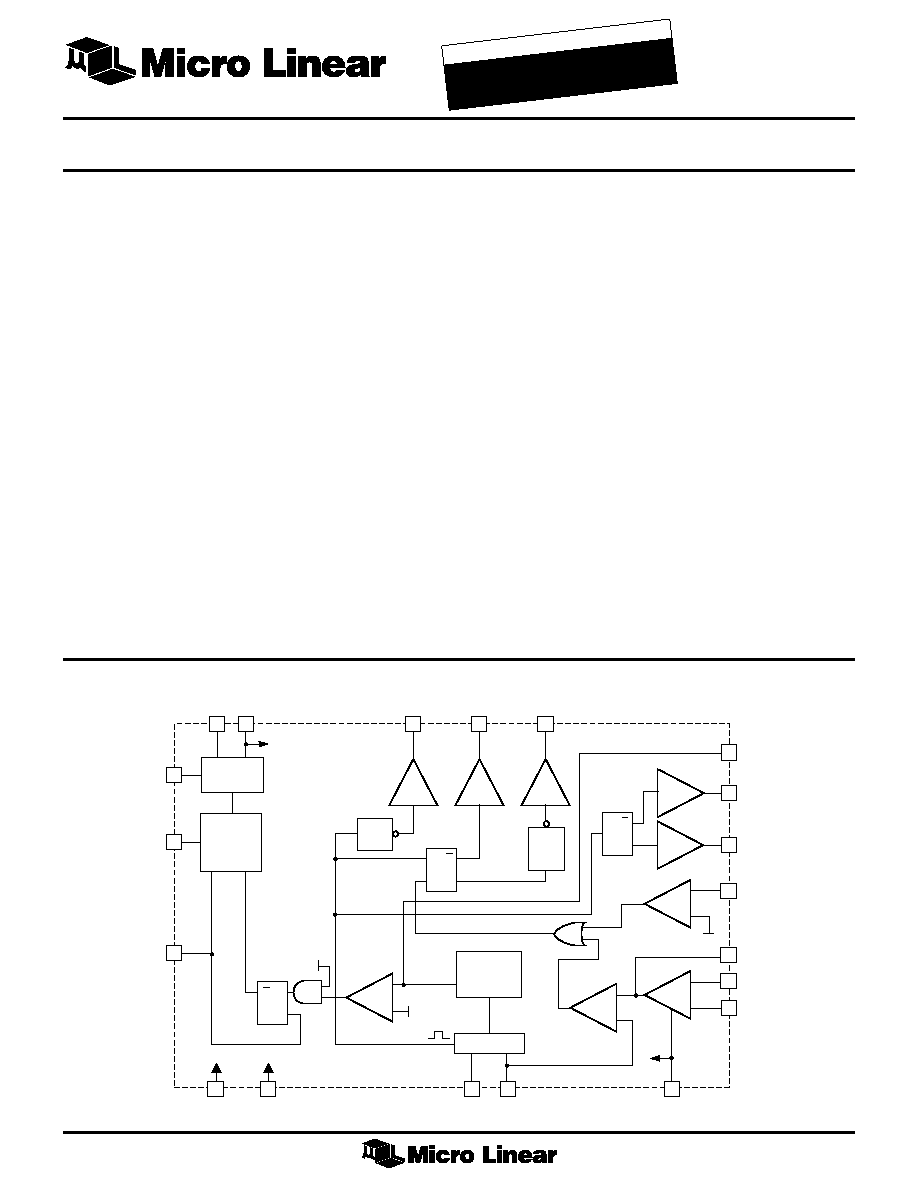
BLOCK DIAGRAM
FEATURES
s
Ideal for 30W inverter designs, 1 to 8 lamp design
s
PWM dimming capability
s
Backlight lamp driver with differential drive
s
Up to 30% lower power for same light output
s
Low standby current (<10µA)
s
Improved efficiency (
ª95%)
s
Allows all N-channel MOSFET drive
s
Adjustable lamp out detect with latch
s
Resonant threshold detection and synchronous
rectification
s
Positive input for dimming control
LINEAR
REGULATOR
MASTER
BIAS
&
UVLO
12
5
13
VDD
VDD
AZR
15
+
≠
VDD
10
B ON
19
B OFF
20
11
DR3
DR1
DR1
Q
Q R
S
OSCILLATOR
CLK
9
≠
+
≠
+
3
7
T
Q
Q
14
16
DR2
DR2
L RTD
L GATE 1
L GATE 2
LEA≠
SS CAP
C
T
ON/OFF
VREF
HVDD
2
17
PGND
18
GND
1
4
R
T
8
LEA OUT
0.5V
6
L ILIM
B SYNC OUT
≠
+
RESONANT
THRESHOLD
DETECTOR
NEG
EDGE
DELAY
S
R Q
Q
ONE
SHOT
LEA+
SS
SS
* THIS PART IS END OF LIFE AS OF J
ULY 1, 2000
NEW!
30W CCFL Inverter Design
ML4877
2
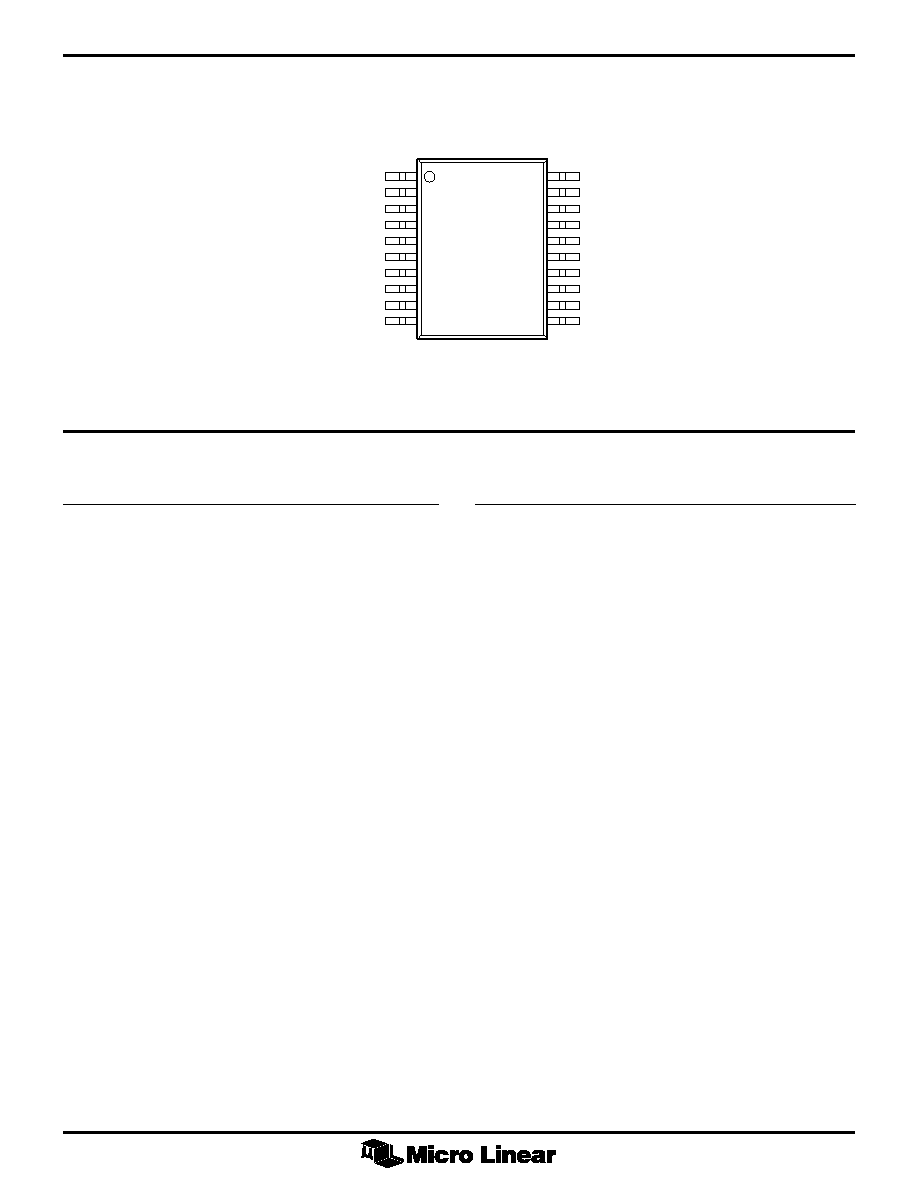
PIN CONFIGURATION
PIN DESCRIPTION
PIN
NAME
FUNCTION
1
LEA+
Positive input for lamp error amp
2
AZR
Connection to gate of external FET for
high voltage regulator. Internally a
zener diode to ground.
3
SS CAP
Connection of optional external soft
start capacitor
4
R
T
Oscillator timing resistor
5
VREF
Voltage reference output
6
L ILIM
Input to current limit amplifier
7
LEA-
Negative input for lamp error
amplifier
8
LEA OUT
Output of lamp error amplifier.
External compensation capacitor
connects between this pin and LEA.
9
C
T
Oscillator timing capacitor
10
L RTD
Input to resonant threshold detector
PIN
NAME
FUNCTION
11
B SYNC
Output of MOSFET driver to gate of
OUT
synchronous FET catch diode.
12
HVDD
Battery power input to linear regulator
13
VDD
Output of linear regulator. Positive
power for IC.
14
L GATE1
Output of MOSFET driver. Connection
to gate of one side of inverter FET
drive pair.
15
ON/OFF
Logic input for chip
16
L GATE2
Output of MOSFET driver. Connection
to gate of one side of inverter FET
drive pair.
17
PGND
Power ground
18
GND
Signal ground
19
B ON
Connection to primary side of gate
pulse transformer
20
B OFF
Output of MOSFET driver. Connection
to gate of FET that disables the input
power.
B OFF
B ON
GND
PGND
L GATE 2
ON/OFF
L GATE 1
VDD
HVDD
B SYNC OUT
1
2
3
4
5
6
7
8
9
10
20
19
18
17
16
15
14
13
12
11
LEA+
AZR
SS CAP
RT
VREF
L ILIM
LEA≠
LEA OUT
CT
L RTD
TOP VIEW
ML4877
20-Pin SSOP (R20)
ML4877
3
ELECTRICAL CHARACTERISTICS
Unless otherwise specified, VDD = 5V ±5%, T
A
= Operating Temperature Range, C
T
= 47pF, R
T
= 82k
W (Note 1)
SYMBOL
PARAMETER
CONDITIONS
MIN
TYP
MAX
UNITS
CURRENT REGULATOR
ERROR AMPLIFIER
Open Loop Gain
60
70
dB
Output High
I
LOAD
= 5µA
2.8
3.0
V
Output Low
I
LOAD
= 25µA
0.4
0.7
V
Bandwidth (-3dB)
1
MHz
Common Mode Voltage Range
0
1.0
V
Input Bias Current
50
100
nA
Input Offset Voltage
-5
0
5
mv
Soft Start Charge Current
V
SSCAP
= 1V
550
750
950
nA
Soft Start Threshold (LEA OUT)
V
SSCAP
= 1V
2
2.5
V
CURRENT LIMIT COMPARATOR
Current Threshold
450
500
550
mV
Input Bias Current
V
ILIM
= 0.1V
50
100
nA
Propagation Delay
(Note 2)
150
250
ns
OUTPUT DRIVERS
Output High - B SYNC OUT, B OFF
VDD 5V, I
LOAD
= 12mA
4.625
4.8
V
Output Low - B SYNC OUT, B OFF
I
LOAD
12mA
0.2
0.375
V
Rise & Fall time - B SYNC OUT, B OFF
C
LOAD
=100pF
20
50
ns
Output High - B ON
VDD 5V, I
LOAD
= 12mA
4.625
4.8
V
Output Low - B ON
I
LOAD
50mA
0.2
0.375
V
Fall Time - B ON
C
LOAD
= 2400pF (Note 2)
45
80
ns
ONE SHOT
Pulse Width
100
150
200
ns
ABSOLUTE MAXIMUM RATINGS
Absolute maximum ratings are those values beyond which
the device could be permanently damaged. Absolute
maximum ratings are stress ratings only and functional
device operation is not implied.
Supply Current (I
CC
) ............................................... 75mA
Output Current, Source or Sink ............................. 250mA
Voltage on Pins LEA+, AZR, SS CAP, R
T
, VREF,
L ILIM, LEA-, LEA OUT, C
T
, B SYNC OUT, VDD,
L GATE 1, ON/OFF, L GATE 2, PGND, GND,
B ON, B OFF ............................... ≠0.3V to VDD +0.3V
Voltage on HVIDD .................................................... 20V
Current into L RTD ............................................... ±10mA
Junction Temperature .............................................. 150∫C
Storage Temperature Range ....................... -65∫C to 150∫C
Lead Temperature (Soldering 10 sec.) ..................... 260∫C
Thermal Resistance (
q
JA
) .................................... 100∫C/W
OPERATING CONDITIONS
Temperature Range
ML4877C ................................................... 0∫C to 70∫C
ML4877E...............................................≠20∫C to 70∫C
ML4877
4
SYMBOL
PARAMETER
CONDITIONS
MIN
TYP
MAX
UNITS
DELAY TIMER
Delay Time
20
35
55
ns
HIGH VOLTAGE INVERTER
Oscillator
Nominal Frequency
68
80
92
kHz
Discharge Current
V
CT
= 2V
500
700
900
µA
Peak Voltage
2.3
2.5
2.7
V
Valley Voltage
0.8
1
1.2
V
Output Drivers
Output High - L GATE 1, 2
VDD = 5V, I
LOAD
12mA
4.625
4.8
V
Output Low - L GATE 1, 2
I
LOAD
= 50mA
0.2
0.375
V
Rise & Fall Time - L GATE 1, 2
C
LOAD
=1000pF
20
50
ns
Resonant Threshold Detector
Threshold
0.45
0.8
1.15
V
Hysteresis
0.15
03
0.45
mV
Lamp Out Detect
Threshold
-2
VDD
2
%
Latch Inhibit Threshold (SSCAP)
LRTD > VDD + 0.1V
2.5
V
Under Voltage Detector
Start Up Threshold
3.8
4.1
4.4
V
Hysteresis
150
300
450
mV
Logic Interface (ON/OFF)
V
IH
2.5
V
V
IL
0.5
V
Input Bias Current
ON/OFF = 3V
10
25
µA
Linear Regulator
Aux Zener Reference Voltage (AZR)
I
AZR
= 10µA
12.3
13.5
14.7
V
Regulator Voltage (VDD)
HVDD = 12V
4.75
5.0
5.35
V
Regulator Source Current
External to device
10
mA
Drop Out Voltage
I
HVDD
= 1mA
30
90
mA
Drop Out Voltage
l
HVDD
= 5mA
125
275
mA
HVDD Input Voltage Range
5
18
V
ELECTRICAL CHARACTERISTICS
(Continued)
ML4877
5
Note 1:
Limits are guaranteed by 100% testing, sampling, or correlation with worst case test conditions.
Note 2:
Actual load is 1200pF. The 2:1 transformer reflects an effective 2400pF.
SYMBOL
PARAMETER
CONDITIONS
MIN
TYP
MAX
UNITS
BIAS
VDD Supply Current
ON/OFF = "I", no load
375
450
µA
VDD Supply Current
ON/OFF = "0", HVDD = 12V
1
10
µA
VREF Load Regulation
I
LOAD
= 25µA
10
20
mV
VREF Output Voltage
T
A
= 25∫C
2.47
2.5
2.53
V
VREF Line Regulation
20
30
mV
VREF Line, Load, Temp
2.465
2.5
2.535
V
ELECTRICAL CHARACTERISTICS
(Continued)

ML4877
6
5 TO 18V
IN
C7
Q1
C3
1.0µF
C8
C9
D1
Q2
T2
C1
*OPTIONAL
SEE NOTE
U2-A
LINEAR
REGULATOR
R1
Q S
Q R
AZR
VDD
VREF
HVDD
SS
PGND
R2
82k
GND
C2
0.1µF
C5
47pF
VDD
B ON
B ON
B SYNC
SS
RT
CT
SS CAP
R4
1.6M
R6
O.5
C6
R7
10k
OPTIONAL
OR
U2-B
L1
100µh
0.1µF
R5
100k
+
≠
+
≠
VDD
ON/OFF
0.5V
C4
LEA OUT
R6
100k
L ILIM
Q4
GATE2
GATE1
L RTD
LEA≠ 0.047µF
ONE
SHOT
RESONANT
THRESHOLD
DETECTOR
DR3
DR1
NEG
EDGE
DELAY
S Q
S Q
OSCILLATOR
DR1
CLK
+
≠
+
≠
DR2
6
10
16
14
T1
LAMP
20
19
2
13
5
4
9
3
17
18
15
MASTER
BIAS
& UVLO
8
1
DR2
11
Q
Q
T
12
7
C11
39pF
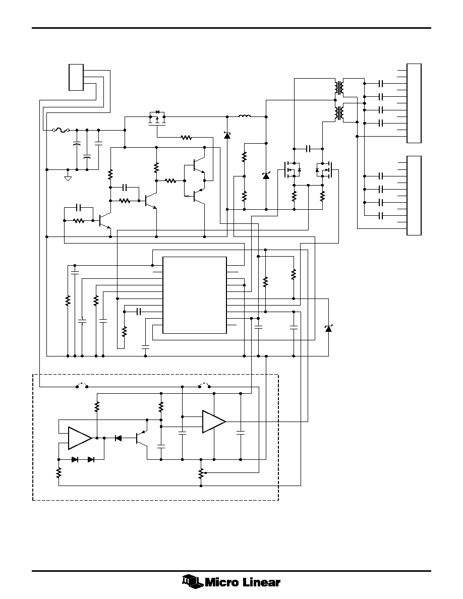
Figure 1. Typical Application Schematic for the ML4877
ML4877
7
FUNCTIONAL DESCRIPTION
The ML4877 consists of a PWM regulator, a lamp driver/
inverter, a linear regulator and control circuits. This IC, in
conjunction with external components, converts a DC
battery voltage into the high voltage and high frequency
AC signal required to start and drive miniature cold
cathode fluorescent lamps. Typical application circuits
are shown in Figure 1 and Figure 5. Note: Please read the
Power Sequencing section below prior to using the
ML4877.
LAMP DRIVER
The lamp driver, sometimes referred to as a lamp inverter,
is comprised of a PWM regulator and a Royer type
inverter circuit to drive the lamp. The PWM regulator, in a
buck configuration, controls the magnitude of the lamp
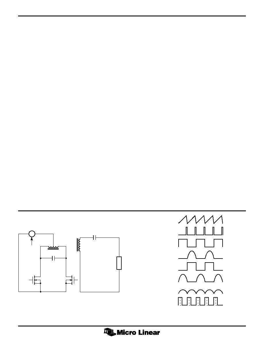
current to provide the dimming capability. Figure 2 shows
a simplified circuit to more easily illustrate the operation
of the circuit.
Due to the presence of the buck inductor, L1, the circuit
shown in Figure 2 is essentially a current fed parallel
loaded resonant circuit. Lm is the primary inductance of
the output transformer, T1, which tunes with the resonant
capacitor C
R
to set the resonant frequency of the inverter.
The oscillator frequency is always set lower than the natural
resonant frequency to ensure synchronization. The current
source IC models the current through the buck inductor L1.
The MOSFETs, (Q3 and Q4) are alternately turned on with
a constant 50% duty cycle signal (L GATE1, L GATE2) at
one-half the frequency of the oscillator. In this way each
transistor pulses, or excites, the resonant tank on each
half cycle. The combination of these two signals appear
across the primary winding of the output transformer as a
sinusoidal waveform. This voltage is multiplied by the
step-up turns ratio of the output transformer and impressed
across the lamp.
The output transitions are controlled by feedback through
the L RTD pin by sensing the voltage at the center tap of
the output transformer. Each time this signal reaches the
minimum resonant threshold detection point an internal
clock pulse is generated to keep the system synchronized.
Figure 3 shows some of these representative waveforms at
the important nodes of the circuit.
The PWM regulator is comprised of a MOSFET (U2-A),
inductor L1, and the gate control and drive circuitry as
shown in Figure 1. A signal with a constant pulse width of
I 50ns is applied to the primary of the 2:1 pulse
transformer T2, rectified by diode D1, and used to charge
the gate capacitance of U2-A, thereby turning it on. The
turn off is controlled by discharging this capacitance
through MOSFET Q2. The pulse width of the signal on the
gate of Q2 (B OFF) varies according to the difference of
the amplitude of the feedback signal on LEA+, and LEA≠.
The signal on LEA≠ is proportional to the AC current
flowing in the lamp, while the signal on LEA+ is a
function of the brightness control setting. The AC lamp
current feedback signal is developed by monitoring the
current through resistor R6 in the common source
connection of the inverter MOSFETs, Q3 and Q4. The
lamp current, and therefore brightness, is adjusted by
varying the voltage applied to R4, at the brightness adjust
control point. Increasing this voltage increases the brightness.
OSCILLATOR
The frequency of the oscillator in the ML4877 is set by
selecting the values Of C
T
and R
T
. Figure 4 shows the
T1
C
OUT
LAMP
©
C
R
Q3
Q4
Lm
Lm
T1
1:N
I
C
Figure 2. Kelvin Sense Connections
SOURCE OF
U2-A
T1-CNTR-PRI
DRAIN-Q3
L GATE2
DRAIN-Q4
L GATE1
C
T
CLOCK
Figure 3. Operating Waveforms
of the Lamp Driver Section

ML4877
8
oscillator frequency versus the value of RT for different
values Of CT. This nomograph may be used to select the
appropriate value of RT and CT to achieve the desired
oscillator frequency for the ML4877.
LINEAR REGULATOR
A linear voltage regulator is provided to power the low
voltage and low current control circuitry on the ML4877.
This is typically used when there is no separate 5V supply
available at the inverter board. For operation up to 18V,
the linear regulator is used by connecting the HVDD pin
to the input battery voltage. For operation over 18V, a
MOSFET, and a resistor (Q and R1, Figure 1) are
connected as shown. The MOSFET is required to stand off
the high voltage. The AZR pin is just a zener diode to
ground used to bias the gate of Q1.
LAMP OUT DETECT
In those cases when there is no lamp connected, or the
connection is faulty, the output voltage of the lamp driver
circuit will tend to rise to a high level in an attempt to
start the nonexistent lamp. The lamp out detect circuit on
the ML4877 will detect this condition by sensing a
voltage proportional to the center tap voltage on the
primary of the output transformer, T1 on the L RTD pin.
The ration of resistors R7 and R8 sets the lamp out detect
threshold. When the voltage on the L RTD pin exceeds
VDD, an internal latch is set and the lamp driver goes
into a shutdown mode. The logic control pin ON/OFF
must be cycled low, then high to reset the latch and
return the lamp driver to the normal state. The input to the
lamp out latch is inhibited by the signal on the soft start
pin. The latch will not be set until the voltage on SS CAP
(pin 3) rises to more than 4.2V nominally.
SOFT START
The capability to control the start up behavior is achieved
by setting the value of a single capacitor, C2 in Figure 1.
FUNCTIONAL DESCRIPTION
(Continued)
1000
100
10
FRQ
UENCY (kHz)
RESISTANCE (k
)
10
100
1000
C = 120pF
C = 81pF
C = 46pF
C = 30pF
Figure 4. Oscillator Frequency Nomograph
By selecting the appropriate value the AC lamp current
can be set to slowly increase with a controlled time
constant. The capacitor value can be calculated
according to the following formula.
C = (3 X 10⁻⁷)TS
(1)
Where TS = Duration of the soft start sequence in seconds
LOGIC CONTROL
The ML4877 is controlled by a single logic input, ON/
OFF. A logic level high on this pin enables the lamp
driver. A logic zero puts the circuit into a very low power
state.
POWER SEQUENCING
It is important to observe correct power and logic input
sequencing when powering up the ML4877. The following
procedure must be observed to avoid damaging the
device.
1. Apply the battery power to HVDD, or
2. If HVDD is not used. Apply the VDD voltage. With
HVDD connected the VDD voltage is supplied by the
internal regulator on the ML4877.
3. Apply a logic high to the ON/OFF input.
Please refer to Application Note 32 for detailed
application information beyond what is presented here.
APPLICATIONS SECTION
HIGH POWER INVERTER
The ML4877 is easily adapted to high power CCFL
inverter designs. Figure 5 displays a schematic of a 30W
ML4877 application. This particular design employs PWM
dimming in order to extend dimming range.
The 30W inverter design is ideal for applications between
the 20W and 30W range. Deep dimming capability is
achieved via PWM technique with no flicker and no pop-
on effects. Uniform intensity can be maintained across 1
to 8 lamps to well below 5%.
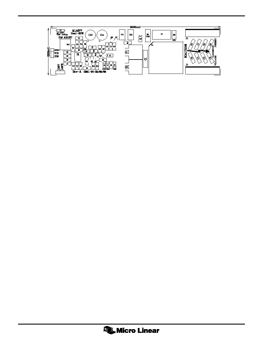
Figure 6 provides a top view of an example of a ML4877
30W design. This design can be modified for 1 to 8 lamps
and contains a PWM dimming interface using standard
low cost components.
For the latest application notes and other information,
visit the Micro Linear website at www.microlinear.com.
ML4877
9
Figure 5. 30W Backlight CCFL Inverter with PWM Dimming
R6
7.5k
B OFF
B ON
GND
PGND
L GATE 2
ON/OFF
L GATE 1
VDD
HVDD
B SYNC OUT
LEA+
AZR
SS CAP
RT
VREF
L ILIM
LEA≠
LEA OUT
CT
L RTD
1
2
3
4
5
6
7
8
9
10
20
19
18
17
16
15
14
13
12
11
ML4877
U2
J1
1
2
3
J2
J3
C2
68pF
C3
68pF
C4
68pF
C5
68pF
C6
68pF
C7
68pF
C8
68pF
C9
68pF
C16
47pF
C19
4.7nF
C18
1nF
C17
4.7nF
C13
1µF
R7
10k
R8
91k
R4
6.2k
C14
1µF
C12
1µF
+
≠
+
≠
R9
143k
R3
10k
5
2
3
1
6
8
4
7
J1
1
2
J2
1
2
C11
1µF
C15
1µF
C10
0.033µF
R2
10k
R6
390k
R1
10k
CR2
1N4148
CR3
1N4148
CR4
1N4148
Q3
2N3906
U1B
U1A
R10
10k
CR1
5.1V
C21
1nF
R13
10k
C23
1nF
R14
1k
R15
1k
R18
200
R16
20
R17
20
Q5
2N3904
Q6
2N3904
Q8
2N3906
Q7
2N3904
Q4
IRF7416
C24
220µF
C20
0.1µF
C22
220µF
F1 4A
T1 1
3
5
12
8
4, 10
9
C1
0.22µF
MKS-10
63V
Q1
IRLR2905
R11
0.2
1W
R5
30k
R12
0.2
1W
Q2
IRLR2905
CR5
CR6
L1
22µH
1
2
3
4
5
6
7
8
9
10
11
1
2
3
4
5
6
7
8
9
10
11
PWM Control
SK34MSCT
1kV
1kV
1kV
1kV
1kV
1kV
1kV
1kV
GND
VDD
DIMMING
ML4877
10
Figure 6. 30W CCFL Inverter Board, 1 to 8 Lamps
ML4877
11
© Micro Linear 1998.
is a registered trademark of Micro Linear Corporation. All other trademarks are the property of their respective owners.
Products described herein may be covered by one or more of the following U.S. patents: 4,897,611; 4,964,026; 5,027,116; 5,281,862; 5,283,483; 5,418,502;
5,508,570; 5,510,727; 5,523,940; 5,546,017; 5,559,470; 5,565,761; 5,592,128; 5,594,376; 5,652,479; 5,661,427; 5,663,874; 5,672,959; 5,689,167; 5,714,897;
5,717,798; 5,742,151; 5,747,977; 5,754,012; 5,757,174; 5,767,653; 5,777,514; 5,793,168; 5,798,635; 5,804,950; 5,808,455; 5,811,999; 5,818,207; 5,818,669;
5,825,165; 5,825,223. Japan: 2,598,946; 2,619,299; 2,704,176; 2,821,714. Other patents are pending.
Micro Linear reserves the right to make changes to any product herein to improve reliability, function or design. Micro Linear does not assume any liability
arising out of the application or use of any product described herein, neither does it convey any license under its patent right nor the rights of others. The circuits
contained in this data sheet are offered as possible applications only. Micro Linear makes no warranties or representations as to whether the illustrated circuits
infringe any intellectual property rights of others, and will accept no responsibility or liability for use of any application herein. The customer is urged to consult
with appropriate legal counsel before deciding on a particular application.
10/29/98 Printed in U.S.A.
ORDERING INFORMATION
PART NUMBER
TEMPERATURE RANGE
PACKAGE
ML4877CR (END OF LIFE)
0∞C to 70∞C
Molded SSOP (R20)
ML4877ER (OBSOLETE)
≠20∫C to 70∫C
Molded SSOP (R20)
2092 Concourse Drive
San Jose, CA 95131
Tel: (408) 433-5200
Fax: (408) 432-0295
www.microlinear.com
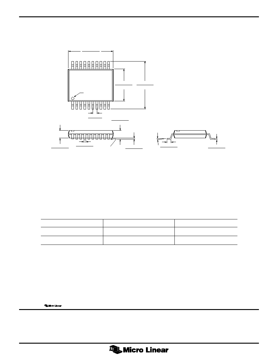
PHYSICAL DIMENSIONS
inches (millimeters)
Package: R20
20-Pin SSOP
SEATING PLANE
0.205 - 0.213
(5.20 - 5.40)
0.301 - 0.313
(7.65 - 7.95)
0.279 - 0.289
(7.08 - 7.34)
0.009 - 0.015
(0.23 - 0.38)
0.026 BSC
(0.65 BSC)
0.022 - 0.038
(0.55 - 0.95)
0.068 - 0.078
(1.73 - 1.98)
0.002 - 0.008
(0.05 - 0.20)
0.066 - 0.070
(1.68 - 1.78)
0.004 - 0.008
(0.10 - 0.20)
0∫ - 8∫
PIN 1 ID
20
1
DS4877-01