
ML5800
5.8GHz Low-IF 1.5Mbps FSK Transceiver
FINAL Datasheet
DS5800-F-02
MARCH 2004
GENERAL DESCRIPTION
The ML5800 is a high integration 5.8GHz Frequency
Shift Keyed (FSK) transceiver that integrates all
frequency generation, receive, and transmit functions
required to realize a digital cordless telephone. Only a
power amplifier (PA) and antenna switch are required to
form a complete 5.8GHz digital radio. The ML5800
operates in the 5.725 to 5.850 GHz unlicensed ISM
band. It can be used to implement both Direct
Sequence and Frequency Hopping Spread Spectrum
radios.
The ML5800 contains a dual-conversion low-IF receiver
with all channel selectivity on chip. IF filtering, IF gain,
and demodulation are performed on chip eliminating
the need for any external IF filters or production tuning.
A post detection filter and a data slicer are integrated to
complete the receiver.
The ML5800 transmitter uses an adjustment-free two-
port closed loop modulator, which modulates the on-
chip VCO with filtered data. An upconversion mixer and
buffer/predriver produces output of 0dBm at 5.8GHz. A
fully integrated 3.9GHz fractional synthesizer is used in
both receive and transmit modes. Power supply
regulation is included in the ML5800, providing circuit
isolation and consistent performance over supply
voltages between 2.7V-3.6V.
PIN CONFIGURATION
VCCA
VCCRF
GNDTX
TXO
RXI
VCCLNA
VCCRXMIX
GNDMIX
XCEN
RXON
PAON
EN
DATA
CLK
AOUT_TPC
VSS
FREF
VCCPLL
QPO
GNDPLL
VCCB
VCCVCO
VTUNE
GNDLO
DOUT
VDD
DIN
VC
CIF
RSSI
VCCTXMIX
VBG
GNDIF
PIN 1
ORDERING INFORMATION
PART NUMBER TEMP RANGE
PACKAGE
PACK (QTY)
ML5800DM
-10
o
C to +60
o
C 32 LPCC 5x5 mm Antistatic Tray (490)
ML5800DM-T
-10
o
C to +60
o
C 32 LPCC 5x5 mm Tape & Reel (2500)
FEATURES
�
High Integration 5.8GHz FSK Transceiver
�
High data rate - 1.536Mbps
�
Low-IF receiver eliminates external IF filters
�
Fully integrated IF filters, FM discriminator, and
data filters
�
Self-calibrated filters eliminate production tuning
�
4dB (typ) Input-referred Noise Figure
�
-94dBm (typ) sensitivity @ 0.1% BER
�
0dBm (typ) Output Power
�
Simple 3-wire Control Interface
�
PA sequencing & integrated pin diode driver
�
Analog RSSI output over a 68dB range
�
Auxiliary switch for transmit power control
�
Space saving 32 pin LPCC package
APPLICATIONS
�
Digital Cordless Telephones
�
Wireless Streaming Audio and Video
�
Game Controllers
�
High-speed Data Links
BLOCK DIAGRAM
Filter
Alignment
PLL
Divider
TXO
5.8GHz
Output
Quadrature
Downmixers
3.9 GHz
VCO
PLL Loop
Filter
Digital
Output
Transmit
Data
Input
Ref.
Divider
Control
Registers
Serial
Control
Bus
RSSI
P.D.
Frequency
Reference
Mode
Control
Control
lines
Quadrature
Generation
Two-port
Modulator
F
to
V
RSSI
RXI
5.8GHz
Input
PAON
RXON
XCEN
DATA
CLK
EN
VTUNE
QPO
Transmit
Mixer
DIN
FREF
DOUT
Receive
Signal
Strength
Indicator
Receiver
Mixer
Analog
Output
AOUT_TPC
Top View

ML5800
DS5800-F-02
FINAL DATASHEET
MARCH 2004
2
TABLE OF CONTENTS
GENERAL DESCRIPTION............................................................................................................................................1
PIN CONFIGURATION .................................................................................................................................................1
ORDERING INFORMATION .........................................................................................................................................1
FEATURES....................................................................................................................................................................1
APPLICATIONS.............................................................................................................................................................1
BLOCK DIAGRAM ........................................................................................................................................................1
TABLE OF CONTENTS ................................................................................................................................................2
ELECTRICAL CHARACTERISTICS .............................................................................................................................3
PIN DESCRIPTIONS ....................................................................................................................................................5
MODES OF OPERATION ...........................................................................................................................................12
CONTROL INTERFACES ...........................................................................................................................................14
TRANSMIT & RECEIVE DATA INTERFACES ............................................................................................................17
REGISTER DESCRIPTIONS ......................................................................................................................................18
PHYSICAL DIMENSIONS ...........................................................................................................................................23
WARRANTY ................................................................................................................................................................24
SIMPLIFIED APPLICATIONS DIAGRAM
BASEBAND
IC
RXI
T P C
DOUT
DIN
RSSI
FREF
CLK,
DATA,
EN
XCEN,
RXON
2
VCCA
VTUNE
QPO
PA � M L 5803
TXO
3
T/R
SWITCH
ANTENNA
AOUT
ML5800
3
PAON
RXI
17
TXO
14
VCCVCO
21
BATTERY
AND
PROTECTION
CIRCUITS
EN
DATA
CLK
RSSI
9
FREF
7
AOUT_TPC
32
DOUT
28
5
4
6
30
DIN
1
XCEN
2
RXON
15
VTUNE
11
QPO
24
VCCA
PAON
VDD
31
VDD
Figure 1: Simplified ML5800 Application Diagram

ML5800
DS5800-F-02
FINAL DATASHEET
MARCH 2004
3
ELECTRICAL CHARACTERISTICS
ABSOLUTE MAXIMUM RATINGS
Absolute maximum ratings are those values beyond which the device could be permanently damaged. Absolute
maximum ratings are stress ratings only and functional device operation is not implied. Operating the device for any
length of time beyond the operating conditions may degrade device performance and/or shorten operating lifetime.
VCCA, VDD ............................................................................................................................................. VSS-0.3 to 3.6 V
Junction Temperature ............................................................................................................................................... 150�C
Storage Temperature Range.......................................................................................................................-65�C to 150�C
Lead Temperature (Soldering, 10s) .......................................................................................................................... 260�C
OPERATING CONDITIONS
Ambient Temperature Range (T
A
) ................................................................................................................-10�C to 60�C
VCCA Range................................................................................................................................................... 2.7V to 3.6V
VDD Range..................................................................................................................................................... 2.7V to 3.6V
Thermal Resistance (
JA
) ...................................................................................................................................... 36�C/W
Maximum receive RF input power ........................................................................................................................ -10dBm
Unless otherwise specified data is over operating conditions (T
A
= -10�C to 60�C, VCCA = VDD = 2.7V to 3.6V ) and
f
REF
= 6.144MHz, V23PLL=0, at Freq=5779.456 MHz (N=229, P=0).
Typical defined as VCCA = VDD = 3.3V, T
A
= 25�C.
SYMBOL PARAMETER
CONDITIONS
MIN
TYP
MAX
UNITS
POWER SUPPLIES
VCCA
Analog supply voltage
2.7
3.3
3.6
V
VDD
Digital supply voltage
VDD pin (VCCA
VDD always)
2.7
3.3
VCCA
V
V
BG
Bandgap Voltage
VBG(p26), I
O
=0
�
A
1.23
V
V
REG
Regulated Voltage
VCCPLL(p10), VCCRF(p23),
VCCTXMIX(p27), VCCIF(p29), I
O
=0
�
A
2.7
V
V
VCO
VCO Regulated Voltage
VCCVCO(p14), I
O
=0
�
A,
VCCB(p13)=2.7V
2.5
V
I
STBY
Supply current, STANDBY mode
DC supply connected, XCEN low, 25�C
and 3.0V
0.1
�
A
I
RX
Supply current, RECEIVE mode
RX chain active, data being received
65
90
mA
I
TX
Supply current, TRANSMIT mode
P
OUT
=0dBm
60
80
mA
SYNTHESIZER
f
C
Carrier frequency range
5.725
5.850
GHz
f
Channel Spacing
512KHz Steps
I
P
Charge Pump sink/source current
�0.22
�0.52
�1.2
mA
F
N
Phase noise at driver output
f
o
=1.2MHz offset from f
c
f
o
=3MHz offset from f
c
f
o
>7MHz offset from f
c
-90
-110
-120
dBc/Hz
dBc/Hz
dBc/Hz
t
FH
Lock time for channel switch
(2.560MHz channels)
From EN asserted to RX valid data(RX),
or PAON high (TX)
1 Channel
5 Channels
Full Range
110
185
250
�
s
�
s
�
s
t
TX2RX
Lock time for TX/RX
RXON High to Valid RX data
70
�
s

ML5800
DS5800-F-02
FINAL DATASHEET
MARCH 2004
4
SYMBOL PARAMETER
CONDITIONS
MIN
TYP
MAX
UNITS
t
RX2TX
Lock time for RX/TX
RXON Low to PAON high
62.5
�
s
t
WAKE
Lock up time from standby
XCEN high to Valid RX data, XCEN low
period >120 seconds
275
�
s
f
FREF
Reference signal frequency
6.144
12.288
MHz
MHz
V
FREF
Reference signal input level
6.144MHz or 12.288MHz sine wave,
capacitively coupled
2.0
VCCA
V
P-P
RECEIVER
Z
in
, S
11
Input Impedance
at RXI
24.5+j28
NF
Input noise figure
5.725-5.850 GHz at RXI
4.0
dB
G
RX
RX Gain
5.725-5.850 GHz, RXI to Limiter
80
dB
DR
RX
Data Rate
1.536
Mbps
S
Input Sensitivity
<0.1% BER
-94
dBm
BW
RX
RX Data Filter 3dB Bandwidth
Gaussian 5
th
order
768
kHz
P
IMAX
Maximum RX RF input
<0.1% BER at 1.536Mbit/sec
-10
dBm
IIP3
RX RF input IP3
Test tones 2 and 4 channels away
-27
dBm
P
RXI
LO leakage at RXI
At 5.8GHz
-50
dBm
IRR
RX Chain Image rejection ratio
35
dB
ACR
RX adjacent channel(s) rejection.
2.56MHz channel spacing
Wanted at -80dBm
1 channel
2 channels
3 or more channels
15
40
45
dB
dB
dB
RECEIVE LOW IF FILTERS
f
IFC
IF filter center frequency
Post-alignment
1.024
MHz
BW
IFC
IF filter 3dB bandwidth
Post-alignment
1.408
MHz
LIMITER, AGC, AND FM DEMODULATOR
t
OVLD
Recovery from overload
Transition time to switch from Pin = �
10dBm input to Pin = �90dBm, time to
valid RX data
20
�
s
Co-Channel rejection, 0.1% BER
Wanted at CHx -80 dBm, unwanted at
CHx modulated with 1.536Mbps GFSK,
BT=0.5, PRBS data
-20
dB
V
ODC
Quiescent output voltage @
AOUT_TPC(pin 7), AOUT Mode
1.15
V
V
OPK
Output voltage swing
AOUT_TPC(pin 7), AOUT Mode
0.8
V
P-P
RSSI
t
R_RSSI
RSSI rise time. < -100dBm to
-15dBm into the RF mixer
20pF loading on the RSSI output. Rise
time from 20% to 80%
5
�
s
t
F_RSSI
RSSI fall time. �15dBm to
< -100dBm into the IF mixer
20pF loading on the RSSI output. Fall
time from 80% to 20%
5
�
s
V
RSMX
RSSI maximum voltage
-10 dBm into RXI
2.7
V
V
RSMD
RSSI midrange voltage
-40 dBm into RXI
2.5
V
V
RSMN
RSSI minimum voltage
No signal applied
0.2
V
V
RSMXC
RSSI maximum voltage (clipped)
-10 dBm into RXI
2.3
V
G
RSSI
RSSI sensitivity
(V
-40dBm
� V
-50dBm
)/10dB
35
mV/dB
RSSI accuracy
Deviation from best fit straight line
�3
dB

ML5800
DS5800-F-02
FINAL DATASHEET
MARCH 2004
5
SYMBOL PARAMETER
CONDITIONS
MIN
TYP
MAX
UNITS
TRANSMITTER
Z
out
S
22
Output Impedance
at TXO
22.5+j3
Matched into 50 ohms, 25C and 3.3V
-4
0
3
P
OUT
TX buffer output power at 5.8 GHz
Matched into 50 ohms, over operating
temperature and voltage range
-7
0
3
dBm
f
DEV
Transmit Modulation Deviation
TXO pin See Figure 6
�512
KHz
BW
TX
TX Data Filter 3dB Bandwidth
1.4
MHz
P
SPUR
TX spurious
-25
dBc
P
IMAGE
TX Image
2/3 F
TXO
, 1/3 F
TXO
-20
dBc
INTERFACE LOGIC LEVELS
Input pins (DIN, XCEN, RXON, DATA, CLK, EN)
V
IH
Input high voltage
VDD*0.7
VDD+0.4
V
V
IL
Input low voltage
-0.4
VDD*0.3
V
I
B
Input bias current
All states
-5
5
�
A
C
IN
Input capacitance
1MHz test frequency
4
pF
Output pins (AOUT_TPC, PAON, DOUT)
V
OL
AOUT open-drain voltage
I
O
=100
�
A, TPC Mode
0.4
V
V
OH
PAON (PA control) output high voltage
Sourcing 5.0 mA
VDD-0.4
V
V
OL
PAON (PA control) output low voltage
Sinking 5.0 mA
0.4
V
I
o
PAON source/sink current
�5.0
�8.0
mA
V
OH
DOUT (data output) output high voltage
Sourcing 0.1 mA
VDD�0.4
V
V
OL
DOUT (data output) output low voltage
Sinking 0.1 mA
0.4
V
3 WIRE SERIAL BUS TIMING
t
r
CLK input rise time (note 1)
15
ns
t
f
CLK input fall time (note 1)
15
ns
t
ck
CLK period
50
ns
t
ew
EN pulse width
200
ns
t
l
Delay from last clock rising edge to rise
of EN
15
ns
t
se
EN setup time to ignore next rising CLK
15
ns
t
s
DATA-to-CLK setup time
15
ns
t
h
DATA-to-CLK hold time
See Figure 5
15
ns
Note 1: Serial I/O clock maximum rise and fall times are based on the minimum clock period. Longer rise and fall times
can be accommodated for slower clocks provided the rise and fall times remain less than 20% of the clock period and
all set up and hold time minimums are met with respect to the CMOS switching points (V
IL
MAX and V
IH
MIN). The
serial I/O clock rise and fall times are limited to an absolute maximum of 100ns.

ML5800
DS5800-F-02
FINAL DATASHEET
MARCH 2004
6
PIN DESCRIPTIONS
PIN
SIGNAL
NAME
I/O
FUNCTION
DIAGRAM
POWER & GROUND
8
VSS
GND
Digital Ground. Ground for digital I/O circuits
and control logic.
N/A
10
VCCPLL
PWR/O
(Decouple
only)
PLL Supply. DC power supply decoupling
point. This pin is connected to the output of
the regulator and to the PLL supplies. A
capacitor must be tied between this pin and
ground to decouple (bypass) noise and to
stabilize the regulator.
See Pin 11 below.
12
GNDPLL
GND
Ground for the PLL.
N/A
13
VCCB
PWR/I
(Regulated
Input)
Regulated DC Power Supply Input to the VCO
voltage regulator. Must be connected to
VCCIF (pin 29) via decoupling network.
N/A
14
VCCVCO
PWR/O
(Decouple
only)
DC power supply decoupling point for the
VCO. Connected to the output of the VCO
regulator. A capacitor must be tied between
this pin and ground to decouple (bypass)
noise and to stabilize the regulator.
N/A
16
GNDLO
GND
DC ground for VCO and LO circuits.
N/A
N/A
GNDDB
GND
Ground for exposed die paddle.
See Pin 20 below
18
VCCRXMIX
PWR/I
(Regulated
Input)
Regulated RX mixer DC supply input. A
capacitor must be tied between this pin and
ground to decouple (bypass) noise. Must be
connected to VCCTXMIX (pin 27).
N/A
19
VCCLNA
PWR/I
(Regulated
Input)
Regulated DC Power supply input to the LNA.
A capacitor must be tied between this pin and
ground to decouple (bypass) noise. Must be
connected to VCCTXMIX (pin 27).
N/A
17
GNDMIX
GND
Signal ground for the receive mixers.
N/A
22
GNDTX
GND
Signal ground for the transmitter.
N/A
23
VCCRF
PWR/O
(Decouple
only)
DC power supply decoupling point for the LO
chain. Connected to the output of a regulator.
A capacitor must be tied between this pin and
ground to decouple (bypass) noise and to
stabilize the regulator.
N/A
24
VCCA
PWR/I
(Unregulated
Input)
Unregulated DC power supply input to voltage
regulators and unregulated loads: 2.7 to 3.6V.
VCCA is the main (or master) analog VCC pin.
There must be capacitors to ground from this
pin to decouple (bypass) supply noise.
N/A
25
GNDIF
GND
DC ground to IF circuits.
N/A
26
VBG
PWR/O
(Decouple
only)
Bandgap decouple voltage. Decoupled to
ground with a capacitor.
N/A
27
VCCTXMIX
PWR/O
(Regulated
Output)
DC power supply output and decoupling point
for TX mixer regulator. A capacitor must be
tied between this pin and ground to decouple
(bypass) noise and to stabilize the regulator.
N/A
29
VCCIF
PWR/O
DC power supply output and decoupling point
for the IF regulator. A capacitor must be tied
N/A

ML5800
DS5800-F-02
FINAL DATASHEET
MARCH 2004
7
PIN
SIGNAL
NAME
I/O
FUNCTION
DIAGRAM
(Regulated
Output)
for the IF regulator. A capacitor must be tied
between this pin and ground to decouple
(bypass) noise and to stabilize the regulator.
31
VDD
PWR/I
(Unregulated
Input)
DC digital power supply input to the interface
logic and control registers. This supply is not
connected internally to any other supply pin,
but its voltage must be less than or equal to
the VCCA supply and greater than or equal to
2.7V. A capacitor must be tied between this
pin and ground to decouple (bypass) noise.
N/A
TRANSMIT/RECEIVE
20
RXI
I (analog)
Receive RF Input. A simple matching network
is required for optimum noise figure. This input
connects to the base of an NPN transistor and
should be AC coupled.
GNDDB
(PIN 24)
(PIN 8)
VSS
RXI
VCCA
0.7V
VCCA
VSS
4k
20
8
24
21
TXO
O (analog)
TX RF open-collector output. 0 dBm nominal
output power into a matched load over 5.725
to 5.850GHz range. This output requires a DC
path to VCCA.
TXO
21
GNDDB

ML5800
DS5800-F-02
FINAL DATASHEET
MARCH 2004
8
PIN
SIGNAL
NAME
I/O
FUNCTION
DIAGRAM
DATA
7
AOUT_TPC
O (analog)
Multi-function Output. In Analog output mode
this output drives an off chip data slicer. In
Transmit power control mode this is an open
drain output, which is pulled low when the
TPC bit (R0:B7) is set to 0. Transitions on
TPC are synchronized to the falling edge of
RXON (Rx to Tx transition).
31
VSS
VDD
100
7
AOUT
8
TPQ
MUX
VSS
8
TPC
MUX
TPC
AOUT
MUX
30
DIN
I (CMOS)
Transmit Data Input. Drives the transmit pulse
shaping circuits. Serial digital data on this pin
becomes FSK modulation on the Transmit RF
output. The logic timing on this pin controls
data timing. Internal circuits determine the
modulation deviation. This is a standard
CMOS input referenced to VDD and VSS.
See Pin 1 below.
32
DOUT
O (CMOS)
Serial digital output after demodulation, chip
rate filtering and center data slicing. A CMOS
level output (VSS to VDD) with controlled slew
rates. A low drive output designed to drive a
short PCB trace and a CMOS logic input while
generating minimal RFI. The internal data
slicer is limited to 0 or 1 run lengths of less
than 3uS.
31
VSS
VDD
250
32
DOUT
8
MODE CONTROL AND INTERFACE LINES
1
XCEN
I (CMOS)
Transceiver enable input. Enables the
bandgap reference and voltage regulators
when high. Consumes only leakage current in
STANDBY mode when low. This is a CMOS
input, and the thresholds are referenced to
VDD and VSS.
2
RXON
I (CMOS)
TX/RX Control Input. Switches the transceiver
between TRANSMIT and RECEIVE modes.
Circuits are powered up and signal paths
reconfigured according to the operating mode.
This is a CMOS input, and the thresholds are
referenced to VDD and VSS.
1
VSS
XCEN
VDD
RXON
DIN
2
30
31
8

ML5800
DS5800-F-02
FINAL DATASHEET
MARCH 2004
9
PIN
SIGNAL
NAME
I/O
FUNCTION
DIAGRAM
3
PAON
O (CMOS)
PA Control Output. Enables the off-chip PA at
the correct times in a Transmit slot. Goes high
when transmit RF is present at TXO; goes low
5
�
s before transmit RF is removed from TXO.
This output has 5mA drivers suitable for
driving pin diode switches directly. It also has
optional interlock logic to disable the PA when
the PLL is out of lock.
31
VSS
VDD
3
PAON
8
9
FREF
I (analog)
Input for the 12.288 MHz or 6.144 MHz
reference frequency. This input is used as the
reference frequency for the PLL and as a
calibration frequency for the on-chip filters. An
AC-coupled sine or square wave source drives
this self-biased input. The reference source
must be accurate to 20 PPM.
9
VSS
FREF
VCCA
24
8
40k
40k
11
QPO
O (analog)
Charge Pump Output of the phase detector.
This is connected to the external PLL loop
filter.
10
VSS
VCCPLL
11
QPO
8
15
VTUNE
I (analog)
VCO Tuning Voltage input from the PLL loop
filter. This pin is very sensitive to noise
coupling and leakage currents.
13
VSS
VCCB
3.7k
15
VTUNE
8
2.5V

ML5800
DS5800-F-02
FINAL DATASHEET
MARCH 2004
10
PIN
SIGNAL
NAME
I/O
FUNCTION
DIAGRAM
28
RSSI
O (analog)
Buffered analog RSSI output with a nominal
sensitivity of 35mV/dB.
24
VSS
VCCA
100
28
RSSI
8
TPI
MUX
RSSI
MUX
RSSI
OP
AMP
SERIAL BUS SIGNALS
4
EN
I (CMOS)
Control Bus Enable. Enable pin for the three-
wire serial control bus that sets the operating
frequency and programmable options. The
control registers are loaded on a low-to-high
transition of the signal. Serial control bus data
is ignored when this signal is high. This is a
CMOS input, and the thresholds are
referenced to VDD and VSS.
5
DATA
I (CMOS)
Serial Control Bus Data. 16-bit words, which
include programming data and the two-bit
address of a control register. This is a CMOS
input, and the thresholds are referenced to
VDD and VSS.
6
CLK
I (CMOS)
Serial control bus data is clocked in on the
rising edge when EN is low. This is a CMOS
input; the thresholds are referenced to VDD
and VSS.
31
VSS
VDD
5.5k
4
EN
8
1.7p
5
DATA
6
CLK
ML5800
DS5800-F-02
FINAL DATASHEET
MARCH 2004
11
FUNCTIONAL DESCRIPTION
The ML5800 enables the design and manufacture of low-cost, small yet high-performance digital RF transceivers in the
relatively interference-free 5.8GHz ISM band. Frequency Shift Keying (FSK) is a constant-envelope modulation, which
allows the use of high-efficiency class C power amplifier (such as the ML5803) resulting in longer battery life.
Integrated in the ML5800 is a dual-conversion low-IF receiver with completely integrated filters, all frequency generation
circuits, and transmit circuits. On-chip regulators protect critical circuits from power-supply noise and allow for
consistent performance over the supply voltage range.
The ML5800 transmits and receives 1.536 Mbps FSK data in the 5.725 to 5.850GHz ISM band. The high data rate
allows for direct sequence spread spectrum coding, which increases interference rejection and input sensitivity at the
cost of reduced effective data rate. For example, a 15-chip spreading sequence results in 11.7dB of processing gain
and a `raw' data rate of 102.4Kbps.
The ML5800 contains a dual-conversion low-IF receiver. The first IF frequency of 1.9 GHz gives an image response,
also at 1.9 GHz. An off-chip filter is needed to protect the receiver from this image and from IF feedthrough. The second
IF frequency of 1.024 MHz results in an image response in an adjacent channel. The quadrature image-reject mixer
and low IF filter combine to achieve a typical image rejection of 35 dB. All IF filtering and demodulation are performed
on chip using active filtering, centered at 1.024 MHz. A matched bit-rate filter and data slicer follow the demodulator
and provide sliced data at the DOUT pin. Buffered analog (unsliced) data is available on the AOUT_TPC pin.
The ML5800 transmitter uses a fractional-N PLL and two-port closed loop modulation to accurately impress the FSK
signal on the 5.8GHz carrier. Closed loop modulation techniques allow for continuous transmission or reception of data
without significant frequency drift, making the ML5800 ideal for wireless streaming media applications. A lock-detect
circuit monitors the state of the PLL loop. When the PLL is out of lock the transmitter output is disabled.
The frequency generation circuits are comprised of a fully integrated 3.9GHz VCO local oscillator (LO), dividers, a
phase comparator, and a charge pump for a PLL frequency synthesizer. A fractional-N PLL applies the low frequency
data modulation onto the LO. The LO is halved to generate accurate quadrature signals at 1.9 GHz for the second LO.
The LO PLL is programmed via the three-wire serial bus (CLK, DATA, EN). There is no error checking of the program
data. This bus is functional, and register contents are preserved in STANDBY mode.
Filter
Alignment
PLL
Divider
TXO
5.8GHz
Output
Quadrature
Downmixers
3.9 GHz
VCO
PLL Loop
Filter
Digital
Output
Transmit
Data
Input
Ref.
Divider
Control
Registers
Serial
Control
Bus
RSSI
P.D.
Frequency
Reference
Mode
Control
Control
lines
Quadrature
Generation
Two-port
Modulator
F
to
V
RSSI
RXI
5.8GHz
Input
PAON
RXON
XCEN
DATA
CLK
EN
VTUNE
QPO
Transmit
Mixer
DIN
FREF
DOUT
Receive
Signal
Strength
Indicator
Receiver
Mixer
Analog
Output
AOUT_TPC
Figure 2: ML5800 Block Diagram

ML5800
DS5800-F-02
FINAL DATASHEET
MARCH 2004
12
MODES OF OPERATION
The ML5800 has three key modes of operation:
�
STANDBY:
All circuits powered down, except the control interface (static CMOS)
�
RECEIVE:
Receiver circuits active
�
TRANSMIT:
Transmitter circuits active
MODE CONTROL
The two modes of operational are RECEIVE and TRANSMIT, controlled by RXON. XCEN is the chip enable/disable
control pin, which sets the device in operational or STANDBY modes. The relationship between the parallel control lines
and the mode of operation of the IC is summarized in Table 1.
XCEN
RXON
MODE NAME
FUNCTION
0
X
STANDBY
Control interfaces active, all other circuits powered down
1
1
RECEIVE
Receiver time slot
1
0
TRANSMIT
Transmit time slot
Table 1: Modes of Operation
STANDBY MODE
In STANDBY mode, the ML5800 transceiver is powered down. The only active circuits are the control interfaces, which
are static CMOS to minimize power consumption. The serial control interface and control registers remain powered up
and will accept and retain programming data as long as the VDD and VCCA are present. When exiting STANDBY
mode, remain in RECEIVE mode for at least 62.5
�
s (typ) to allow for filter calibration.
RECEIVE MODE
In RECEIVE mode, the received signal at 5.8 GHz is down converted, bandpass filtered (IF filter), fed to the frequency-
to-voltage converter, and low-pass filtered. The output of the low-pass filter is available at both the AOUT_TPC pin and
to the on-chip data slicer, which outputs NRZ digital data to the DOUT pin. An RSSI voltage output indicates the RF
input signal level at the output of the IF filter.
Receive Signal Strength Indication (RSSI)
RSSI is an indication of field strength. It can be used by the system to determine transmit power control (conserve
battery life) and/or to determine if a given channel is occupied.
Automatic Filter Alignment
When the chip is powered up the tuning information is reset to mid-range. In the first 62.5
�
s of RECEIVE mode (RXON
set high) the ML5800 performs filter self-calibration, which tunes all the internal filters relative to the signal on the FREF
pin. Valid data is received after calibration is completed. Self-calibration sets:
�
Discriminator center frequency
�
IF filter center frequency and bandwidth
�
Receiver data low-pass filter bandwidth
�
Transmit data low-pass filter bandwidth

ML5800
DS5800-F-02
FINAL DATASHEET
MARCH 2004
13
TRANSMIT MODE
In TRANSMIT mode, the PLL loop is closed to eliminate frequency drift. A two-port modulator modulates both the VCO
and the fractional-N PLL. The VCO is directly modulated with filtered FSK transmit data. The PLL is driven by a sigma-
delta modulator, which ensures that the PLL follows the mean frequency of the modulated VCO.
PLL Programming & Channel Selection
The ML5800 PLL is programmed with a 14bit word to set the RF center frequency of the radio. The channel frequency
(f
c
) is given by:
f
c
= 1.5 * 6.144 * (512 +N/2 + (P+11)/18) MHz
Where N is the "integer" portion and P is the "fractional" portion of the synthesizer. See Register 1 Description for
further details on how to program the channel frequency plan in the control register.
ML5800
DS5800-F-02
FINAL DATASHEET
MARCH 2004
14
CONTROL INTERFACES
There are two sets of control interfaces for the ML5800:
�
RF Control:
XCEN, RXON, FREF, RSSI, PAON, AOUT_TPC
�
Serial Bus Control:
EN, DATA, CLK
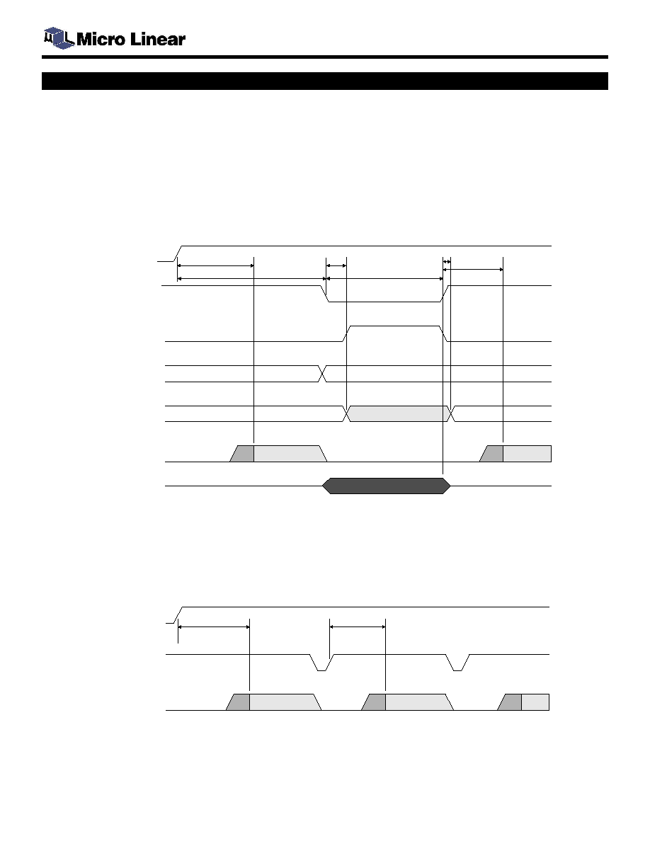
The ML5800 transceiver is used in time division duplex (TDD) mode, where the transceivers at each end of a radio link
alternately transmit and receive. Immediately before data is transmitted or received the ML5800 goes through a `self-
calibration' sequence, where the IF and data filters are frequency aligned while the PLL settles to the carrier frequency.
These calibration cycles are triggered by logic transitions on the control interface. Figure 3 shows the normal operating
cycle for the ML5800.
Tx Data
PAON
RXON
XCEN
t
WAKE
t
RX2TX
DIN
DOUT
TXO
Valid RX Data
t
ED
AOUT_TPC
t
TX2RX
t
MAX
t
MAX
Figure 3: Control Timing for TDD Operation
To implement channel scanning, the ML5800 is kept in RECEIVE mode (XCEN and RXON high) and the PLL is
reprogrammed to select a different RF channel. A filter calibration cycle is initiated by each serial bus write to the
register controlling the PLL modulus, so that filter alignment is updated as the VCO settles to the next programmed
channel frequency. Serial bus writes to other registers do not trigger a calibration cycle. Signal diagram for channel
scanning is shown in Figure 4.
XCEN
DOUT
Valid RX Data
Valid RX Data
EN (Write to PLL
tuning register)
t
WAKE
t
FH
Figure 4: Control Timing when Channel Scanning

ML5800
DS5800-F-02
FINAL DATASHEET
MARCH 2004
15
Table 2 gives the minimum times between transitions on the control interface for the ML5800 transceiver to work
correctly. Times t1, t2, and t4 are the minimum delays that the baseband design must allow before valid receive data is
expected on the DOUT pin.
SYMBOL
PARAMETER
WORST CASE TIMING
UNITS
t
WAKE
Wait time from XCEN asserted to valid Receive data out
325
�
s
t
FH
Time from rising edge of Serial Bus EN to valid Receive data out (channel scan mode, one
channel hop, PLL re-locking triggered by rising EN).
125
�
s
t
TX2RX
Time from rising edge of RXON to valid Receive data out
120
�
s
t
RX2TX
Time from falling edge on RXON to start of valid data on DIN pin. Note that RF energy will
be present on TXO during this period but PAON will be unasserted.
62.5
�
s
t
MAX
Maximum TX or RX time under steady state operating temperatures (<�2�C/minute)
60
s
t
ED
Time from rising edge on RXON to end of valid data on DIN pin (Start of PLL Freq. shift)
6
�
s
Table 2: Transceiver Control Interface Timing
RF CONTROL: XCEN, RXON, FREF, RSSI, PAON & TPC
The XCEN pin enables/disables the ML5800 and places the device in either standby or active modes. The default
power up is in RECEIVE mode.
The RXON pin determines which active mode the ML5800 is in: RECEIVE or TRANSMIT.
The FREF pin is the master reference frequency for the transceiver. It supplies the frequency reference for the RF
channel frequency and the on-chip filter tuning. The FREF pin is a CMOS input with on-chip biasing resistors. It can be
driven by an AC coupled sine-wave source or by a CMOS logic output. FREF is used as a calibration frequency and as
a timing reference in the control circuits. The reference source must be accurate to 20 PPM.
The RSSI pin supplies a voltage that indicates the amplitude of the received RF signal. It is connected to the input of a
low-speed ADC on the baseband IC, and is used during channel scanning to detect clear channels on which the radio
can transmit. The RSSI (Received Signal Strength Indicator) voltage is proportional to the logarithm of the received
power level.
The ML5800 has two output pins that control and sequence the power amplifier (PA): PAON and AOUT_TPC.
The PAON (PA control) is a 5mA CMOS output that controls an off-chip RF PA and T/R switch (can directly drive PIN
diodes). It outputs a logic high when the PA should be enabled and a logic low at all other times. This output is inhibited
when the PLL fails to lock.
When digital data output (DOUT) is used, the AOUT_TPC pin is an open-drain output intended for transmit power
control (TPC). It is configured by Bit 4 in Register 0 (AOUT) and when selected as a TPC output, reflects the state of Bit
7 in Register 0 (TPC). The TPC register bit can be changed at any time, but the AOUT_TPC pin does not change state
until the beginning of the next transmit slot, triggered by a falling edge on RXON. In analog data output mode, the
AOUT_TPC pin becomes the analog data output to an off-chip data slicer.

ML5800
DS5800-F-02
FINAL DATASHEET
MARCH 2004
16
SERIAL BUS CONTROL: EN, DATA, CLK
A 3-wire serial interface is used for programming the ML5800 configuration registers, which control device mode of
operation, pin functions, PLL and reference dividers, internal test modes and filter alignment. Data words are entered
beginning with the MSB. The word is divided into a leading 14-bit data field followed by a 2-bit address field. When the
address field has been decoded the destination register is loaded on the rising edge of EN. Providing less than 16
bits of data will result in unpredictable behavior when EN goes high.
Data and clock signals are ignored when EN is high. When EN is low, data on the DATA pin is clocked into a shift
register by rising edges on the CLK pin. The information is loaded into the addressed latch when EN returns high. This
serial interface bus is an industry standard bus commonly found on PLL devices. It can be efficiently programmed by
either byte or 16-bit word oriented serial bus hardware. The data latches are implemented in CMOS and use minimal
power when the bus is inactive. See Figure 5 and Table 3.
CLK
Data
EN
t
s
t
h
t
r
t
f
t
ck
t
l
t
se
t
ew
MSB
Figure 5: Serial Bus Timing Diagram
SYMBOL PARAMETER
MIN MAX
UNITS
BUS CLOCK (CLK)
t
r
Clock input rise time (note 1)
15
ns
t
f
Clock input fall time (note 1)
15
ns
t
ck
Clock period
50
ns
ENABLE (EN)
t
ew
Minimum pulse width
200
ns
t
l
Delay from last clock rising edge to rise of EN
15
ns
t
se
Enable set up time to ignore next rising clock
15
ns
BUS DATA (DATA)
t
s
Data to clock set up time
15
ns
t
h
Data to clock hold time
15
ns
Table 3: Serial Bus Timing Specifications
Note 1: Serial I/O clock maximum rise and fall times are based on the minimum clock period. Longer rise and fall times
can be accommodated for slower clocks provided the rise and fall times remain less than 20% of the clock period and
all set up and hold time minimums are met with respect to the CMOS switching points (V
IL
MAX and V
IH
MIN). The
serial I/O clock rise and fall times are limited to an absolute maximum of 100ns.

ML5800
DS5800-F-02
FINAL DATASHEET
MARCH 2004
17
TRANSMIT & RECEIVE DATA INTERFACES
There are two sets of transmit and receive data interfaces for the ML5800:
�
Baseband Data:
DIN, DOUT, AOUT
�
RF Data:
RXI, TXO
BASEBAND DATA: DIN, DOUT, AOUT
The DIN pin is a CMOS-level serial data input for FSK modulation on the radio channel. This DIN pin drives data bits
into the two-port transmit modulator. When used with Direct Sequence Spread Spectrum (DSSS), the chip rate, bit rate
and spreading code are determined in the baseband processor and the FM deviation and transmit filtering are
determined in the ML5800. There is no re-timing of the chips, so the transmitted FSK chips take their timing from the
data on this pin.
The DOUT pin is a corresponding CMOS-level digital data output. The data on this pin is valid only when the run length
of the transmitted digital data is limited to consecutive 1's or 0's no longer than 3
�
s.
When longer run lengths are used, an off-chip data slicer is required, driven from the AOUT_TPC pin. Setting the AOUT
bit in Register 0 turns the AOUT_TPC pin into a buffered, single-ended analog output from the data filter. This output
can be used to drive an off-chip data slicer or an ADC input for a DSP data slicer. Clock recovery for both DOUT and
AOUT modes is performed in the baseband.
RF DATA: RXI, TXO
The RXI receive input (pin 20) and the TXO transmit output (pin 21) are the only RF I/O pins. The RXI pin requires a
simple impedance matching network for best input noise figure, and the TXO pin also requires a matching network for
maximum power output into 50
. The voltage on the modulation port swings above and below its central value to
produce 2-FSK modulation on the VCO. (See Figure 6)
For best performance, all RF ground pins must have a direct connection to the RF ground plane, and the RF supply
pins must be well decoupled from the RF ground pins.
F
OS
F
MAX
F
MIN
F
DEV
TRANSIENT TRANSMIT MODULATION Freq=5.779456GHz, VCCA=VDD=3.3V, Ta=25C
NAME
DESCRIPTION
CONDITIONS
MIN
TYP
MAX
Units
F
DEV
Final Modulation Deviation
After 200us of consecutive 1 or 0
bits
�500
�512
�524
kHz
F
MAX
Maximum Modulation
Deviation
PN (15 bit) Sequence Encoded
Data @ 1.536Mb/s
�720
kHz
F
MIN
Minimum Modulation
Deviation
PN (15 bit) Sequence Encoded
Data @ 1.536Mb/s
�450
kHz
F
OS
Modulation center frequency
offset
50us after RXON low
�50
kHz
Figure 6. Transient Transmit Modulation Waveform

ML5800
DS5800-F-02
FINAL DATASHEET
MARCH 2004
18
REGISTER DESCRIPTIONS
A 3-wire serial data input bus sets the ML5800's transceiver parameters and programs the PLL circuits. Entering 16-bit
words into the ML5800 serial interface performs programming. Three 16-bit registers are partitioned such that 14 bits
are dedicated for data to program the operation and two bits identify the register address. The contents of these
registers cannot be read back.
The three registers are:
�
Register 0: PLL Configuration
�
Register 1: RF Channel Frequency Configuration
�
Register 2: Test Mode Access
Figure 7 shows a register map. Table 4 through Table 21 provide detailed diagrams of the register organization: Table
4 outlines the PLL configuration register (Register 0), Table 17 describes the channel frequency register (Register 1),
and displays the filter tuning and test mode register (Register 2).
Res.
DB13
MSB
B15
DB12
B14
DB11
B13
DB10
B12
DB9
B11
DB8
B10
DB7
B9
DB6
B8
DB5
B7
DB4
B6
DB3
B5
DB2
B4
DB1
B3
DB0
B2
ADR1
B1
ADR0
B0
Res.
V23PLL
NOPD
RCLP
LVLO
TXOL
TXM
TPC
TXCW
LOL
AOUT
RD0
QPP
0
0
N9
DB13
MSB
B15
DB12
B14
DB11
B13
DB10
B12
DB9
B11
DB8
B10
DB7
B9
DB6
B8
DB5
B7
DB4
B6
DB3
B5
DB2
B4
DB1
B3
DB0
B2
ADR1
B1
ADR0
B0
N8
N7
N6
N5
N4
N3
N2
N1
N0
P3
P2
P1
P0
0
1
TMODE
DB13
MSB
B15
DB12
B14
DB11
B13
DB10
B12
DB9
B11
DB8
B10
DB7
B9
DB6
B8
DB5
B7
DB4
B6
DB3
B5
DB2
B4
DB1
B3
DB0
B2
ADR1
B1
ADR0
B0
CFB6
CFB5
CFB4
CFB3
CFB2
CFB1
CFB0
DTM2
DTM1
DTM0
ATM2
ATM1
ATM0
1
0
Register 0: PLL Configuration Register
Register 1: RF Channel Frequency Configuration Register
Register 2: Test Mode Access Register
Data
Data
Data
Address
Address
Address
Figure 7: Configuration Register Map
Power-On State
On power up, all register bits are cleared to the default value of 0 (zero). Power up is defined as occurring when VDD =
2.0V. The register default values are valid upon power up.
Register Format
The two least significant bits of every register are the address bits ADR <1:0>. Each register is divided into a data field
and address field. The data field is the leading field, while the last two bits clocked into the register are always the
address field. When EN goes high, the address field is decoded and the addressed destination register is loaded. The
last 16 bits clocked into the serial bus are loaded into the register. Clocking in less than 16 bits may result in an
incorrect entry into the register.
ML5800
DS5800-F-02
FINAL DATASHEET
MARCH 2004
19
REGISTER 0 BIT DESCRIPTIONS
DATA BIT
NAME
DESCRIPTION
USE
B15 (MSB) / DB13
Reserved
Reserved
Set bit to 0
B14 / DB12
Reserved
Reserved
Set bit to 0
B13 / DB11
V23PLL
Low Voltage PLL Regulator
0: PLL Regulator set to 2.7V
1: PLL Regulator set to 2.3V
B12 / DB10
NODP
No Dither
0: 2
nd
order Fractional-N
1: 1
st
order Fractional-N
B11 / DB9
RCLP
RSSI Clip Enable
0: RSSI hardware clipping
1: No RSSI clipping
B10 / DB8
LVLO
Low Voltage Lockout
0: PAON unaffected by low voltage events
1: PAON gated by latched low voltage lockout
B9 / DB7
TXOL
Transmit PLL Mode
0: Closed Loop in Transmit mode
1: Open Loop in Transmit mode
B8 / DB6
TXM
TX RF Output Mode
0: TXO always on in Transmit mode
1: TXO follows PAON signal
B7 / DB5
TPC
Transmit Power Control
0: AOUT pin pulled to ground
1: AOUT pin high impedance
B6 / DB4
TXCW
Transmit Test Mode
0: FSK modulation in Transmit mode
1: CW in Transmit mode (no modulation)
B5 / DB3
LOL
PLL IF Shift Configuration
0: -1.024MHz LO Shift in Receive
1: +1.024MHz LO Shift in Receive
B4 / DB2
AOUT
Analog Output
0: AOUT pin is Transmit Power Control
1: AOUT pin is Analog Data Out
B3 / DB1
RD0
Reference Frequency Select
0: 6.144MHz nominal reference frequency
1: 12.288MHz nominal reference frequency (preferred)
B2 / DB0
QPP
PLL Charge Pump Polarity
0: Fc < Fref; Charge pump sources current
1: Fc < Fref; Charge pump sinks current
B1 / ADR1
ADR1
MSB Address Bit
ADR1 = 0
B0 (LSB) / ADR0
ADR0
LSB Address Bit
ADR0 = 0
Table 4: Register 0 - PLL Configuration Register
QPP
Charge Pump Polarity: This bit sets the charge pump polarity to sink
or source current. For a majority of applications, this bit is cleared
(QPP = 0). For applications where an external inverting amplifier is in
the loop filter, this bit is set to 1 to change the charge pump polarity
(see Table 5).
QPP
PLL CHARGE PUMP POLARITY
0
For Fc < Fref. Charge pump sources current.
1
For Fc < Fref. Charge pump sinks current.
Table 5: PLL Charge Pump Polarity
RD0
Reference Divider: This bit sets the reference divider from the FREF
pin to the reference input of the PLL phase/frequency detector (see
Table 6).
RD0
REFERENCE
DIVISION
NOMINAL REFERENCE
FREQUENCY
0
1
6.144 MHz
1
2
12.288 MHz
Table 6. Reference Frequency Select

ML5800
DS5800-F-02
FINAL DATASHEET
MARCH 2004
20
AOUT
Analog Output Mode: This bit changes the function of the AOUT pin
between an analog data output and transmit power control (see
Table 7).
AOUT
AOUT PIN FUNCTION
0
Transmit Power Control
1
Data Filter Analog Output
Table 7: AOUT Function Select
LOL
PLL IF Shift: This bit shifts the PLL by �1.024MHz in Receive mode
(see Table 8).
LOL
PLL IF SHIFT CONFIGURATION
0
-1.024MHz LO Shift in Receive
1
+1.024MHz LO Shift in Receive
Table 8: PLL IF Shift Configuration
TXCW
Transmit Continuous Wave: This bit produces a continuous wave
(CW) transmitter output for product test when RXON is low (see
Table 9).
TXCW
TRANSMIT MODULATION
0
FSK Modulation
1
CW � No Modulation
Table 9: Transmit Modulation Mode
TPC
Transmit Power Control: When the AOUT bit is low, this bit controls
the state of the open-drain output pin. Although this bit can be
changed at any time, the AOUT pin only changes state at the falling
edge of RXON (see Table 10).
TPC
TPC PIN STATE
0
Pulled to Ground
1
High Impedance
Table 10: TPC Pin State
TXM
Transmit Mode Bit: This bit controls the TX RF buffer state timing
mode. It must be reset to 0 for normal operation (see Table 11).
TXM
TXO BUFFER BEHAVIOR
0
RF Output Always On in TX Mode
1
RF Output Follows PAON
Table 11: TXM Mode
TXOL
Transmit PLL Mode: This bit is provided for testing. It disables the
PLL during transmit slots so that the analog modulation path onto the
VCO can be tested without the digital path through the PLL (see
Table 12).
TXOL
TRANSMIT PLL MODE
0
Closed Loop in TX Mode
1
Open Loop in TX Mode
Table 12: TXOL Operation
LVLO
Low Voltage Lock Out: The LVLO bit enables a transmit low voltage
lockout latch which shuts off the transmitter by de-asserting the
PAON output. This latch is set if the supply voltage drops below
2.65V and is reset when RXON goes high (see Table 13).
LVLO
PAON BEHAVIOR
0
PAON Undisturbed
1
PAON de-asserted when VCCA<2.65V,
Reset by RXON high
Table 13: LVLO Operation
RCLP
RSSI Clip Enable: The RCLP bit disables the RSSI clipping circuitry.
With RCLP low, the RSSI output voltage is clipped at 1.95V (see
Table 14).
RCLP
RSSI BEHAVIOR
0
RSSI output clipped
1
RSSI output not clipped
Table 14: RCLP Operation
NODP
PLL Dithering: This bit removes 2
nd
order dither from the fractional-N
PLL when high, reducing the PLL to a 1
st
order fractional-N (see
Table 15).
NODP
PLL BEHAVIOR
0
2
nd
order Fractional-N PLL
1
1
st
order Fractional-N PLL
Table 15: Dithering Operation
V23PLL
Voltage on PLL Regulator: This bit controls the voltage of the PLL
regulator. It is set to 0 for normal operation. (see Table 17).
V23PLL
REGULATOR BEHAVIOR
0
PLL Regulator set to 2.7V
1
PLL Regulator set to 2.3V
Table 16: V23PLL Mode

ML5800
DS5800-F-02
FINAL DATASHEET
MARCH 2004
21
REGISTER 1 BIT DESCRIPTIONS
DATA BIT
NAME
DESCRIPTION
USE
B15 (MSB) / DB13
N9
B14 / DB12
N8
B13 / DB11
N7
B12 / DB10
N6
B11 / DB9
N5
B10 / DB8
N4
B9 / DB7
N3
B8 / DB6
N2
B7 / DB5
N1
B6 / DB4
N0
PLL Integer Part - N
N = MOD [Floor ((F/4.608) � 0.512 � ((P+11)/18)), 1024]
B5 / DB3
P3
B4 / DB2
P2
B3 / DB1
P1
B2 / DB0
P0
PLL Fractional Part � P
P= MOD [Round (F/0.512 � 11), 9]
B1 / ADR1
ADR1
MSB Address Bit
ADR1 = 0
B0 (LSB) / ADR0
ADR0
LSB Address Bit
ADR0 = 1
Table 17: Register 1 � Channel Frequency Register
This register sets the channel frequency for the ML5800 transceiver.
The "N" Field is the 10-bit integer part of the division ratio, modulo 1024. There is an implicit MSB in the "B16" position
which is fixed to "1". Values from 0 (00 0000 0000b) to 1022 (11 1111 1110b) are all valid and correspond to N =1024 to
N = 2046. The 4-bit "P" field is the fractional part of the division ratio, modulo 9. Values from 0 (0000b) to 8 (1000b) are
valid.
The relationship between N and P with a given channel frequency F is:
F = 1.5 * 6.144 * (512 +N/2 + (P+11)/18) MHz
To calculate N and P from the channel frequency, F (in MHz) use these formulae:
N = MOD [Floor ((F/4.608) � 0.512 � ((P+11)/18)), 1024]
P= MOD [Round (F/0.512 � 11), 9]

ML5800
DS5800-F-02
FINAL DATASHEET
MARCH 2004
22
REGISTER 2 BIT DESCRIPTIONS
DATA BIT
NAME
DESCRIPTION
USE
B15 (MSB) / DB13
TMODE
B14 / DB12
CFB6
B13 / DB11
CFB5
B12 / DB10
CFB4
B11 / DB9
CFB3
B10 / DB8
CFB2
B9 / DB7
CFB1
B8 / DB6
CFB0
Filter Alignment Control Bits
See Table 21
B7 / DB5
DTM2
B6 / DB4
DTM1
B5 / DB3
DTM0
Digital Test Control Bits
See Table 20
B4 / DB2
ATM2
B3 / DB1
ATM 1
B2 / DB0
ATM 0
Analog Test Control Bits
See Table 19
B1 / ADB1
ADR1
MSB Address Bit
ADR1 = 1
B0 (LSB) / ADB0
ADR0
LSB Address Bit
ADR0 = 0
Table 18: Register 2 � Test Mode Access Register
ATM<2:0>
Analog Test Control Bits: The performance of the ML5800 is not specified in these test modes. Although primarily
intended for IC test and debug, they also can help in debugging the radio system. The default (power-up) state of these
bits is ATM<2:0> = <0,0,0>. When a non-zero value is written to the field, the RSSI and AOUT_TPC pins become
analog test access ports, giving access to the outputs of key signal processing stages in the transceiver. During normal
operation, the ATM field must be set to zero (see Table 19).
ATM2 ATM1 ATM0
RSSI
AOUT
0
0
0
RSSI
Set by AOUT bit
0
0
1
Data Filter input +
Data Filter input -
0
1
0
I IF Filter Output
Q IF Filter Output
0
1
1
Q IF Filter � Input
Q IF Filter + Input
1
0
0
I IF Filter � Input
I IF Filter + Input
1
0
1
Data Filter + Output
Data Filter �Output
1
1
0
I IF Limiter Output
Q IF Limiter Output
1
1
1
1.67V Voltage Reference VCO Modulation Port Input
Table 19: Analog Test Control Bits

ML5800
DS5800-F-02
FINAL DATASHEET
MARCH 2004
23
DTM <2:0>
Digital Test Control Bits: The performance of the ML5800 is not specified in these test modes. Although primarily
intended for IC test and debug, they also can help in debugging the radio system. The default (power up) state of these
bits is DTM<2:0> = <0,0,0>. When a non-zero value is written to these fields, the DOUT and PAON pins become a
digital test access port for key digital signals in the transceiver. During normal operation, the DTM field must be set to
zero (see Table 20).
DTM2 DTM1 DTM0
PAON
DOUT
0
0
0
PA Control
Data Out
0
0
1
No Output
AGC Switch State
0
1
0
Prescaler Out Divide 64
PLL Main Divider Output
0
1
1
No Output
PLL Reference Divider Output
1
0
0
PLL 2
nd
Carry Diagnostic o/p
PLL 1
st
Carry Diagnostic o/p
1
0
1
No Output
TCAL (Cal. Timer)
1
1
0
3MHz from PLL
LOCKN
1
1
1
No Output
UDLATCH
Table 20: Digital Test Control Bits
TMODE and CFB <6:0>
The TMODE bit disables the automatic filter alignment circuitry, and then the CFB field directly tunes the filter. The CFB
field is a 7 bit binary value that tunes the IF and data filters. The correct value for CFB6 to CFB0 varies depending
upon absolute values of the integrated resistors and capacitors on the chip. The IF filter center frequency, IF filter
bandwidth, data filter bandwidth and F to V converter center frequency are all tuned together by the CFB field (see
Table 21).
TMODE
FILTER ALIGNMENT MODE
0
Filters auto aligned during receive slots
1
Filters tuned by CFB<6:0> value
Table 21: TMODE and CFB <6:0> Filter Alignment Test Bits
PHYSICAL DIMENSIONS
Figure 8: 32 Leadless Plastic Chip Carrier (LPCC) Dimensions

ML5800
DS5800-F-02
FINAL DATASHEET
MARCH 2004
24
WARRANTY
Micro Linear makes no representations or warranties with respect to the accuracy, utility, or completeness of the
contents of this publication and reserves the right to make changes to specifications and product descriptions at any
time without notice. No license, express or implied, by estoppel or otherwise, to any patents or other intellectual
property rights is granted by this document. The circuits contained in this document are offered as possible applications
only. Particular uses or applications may invalidate some of the specifications and/or product descriptions contained
herein. The customer is urged to perform its own engineering review before deciding on a particular application. Micro
Linear assumes no liability whatsoever, and disclaims any express or implied warranty, relating to sale and/or use of
Micro Linear products including liability or warranties relating to merchantability, fitness for a particular purpose, or
infringement of any intellectual property right. Micro Linear products are not designed for use in medical, life saving, or
life sustaining applications.
If this document is "Advance", its contents describe a Micro Linear
product that is currently under development. All
detailed specifications including pinouts and electrical specifications may be changed without notice. If this document is
"Preliminary", its contents are based on early silicon measurements. Typical data is representative of the product but is
subject to change without notice. Pinout and mechanical dimensions are final. Preliminary documents supersede all
Advance documents and all previous Preliminary versions. If this document is "Final", its contents are based on a
characterized product, and it is believed to be accurate at the time of publication. Final Data Sheets supersede all
previously published versions. This document is Final.
� 2004 Micro Linear Corporation. All rights reserved. All other trademarks are the property of their respective owners.
Products described herein may be covered by one or more of the following U.S. patents: 4,897,611; 4,964,026;
5,027,116; 5,281,862; 5,283,483; 5,418,502; 5,508,570; 5,510,727; 5,523,940; 5,546,017; 5,559,470; 5,565,761;
5,592,128; 5,594,376; 5,652,479; 5,661,427; 5,663,874; 5,672,959; 5,689,167; 5,714,897; 5,717,798; 5,742,151;
5,747,977; 5,754,012; 5,757,174; 5,767,653; 5,777,514; 5,793,168; 5,798,635; 5,804,950; 5,808,455; 5,811,999;
5,818,207; 5,818,669; 5,825,165; 5,825,223; 5,838,723; 5.844,378; 5,844,941. Japan: 2,598,946; 2,619,299;
2,704,176; 2,821,714. Other patents are pending.
cQ
Micro Linear Corporation
2050 Concourse Drive
San Jose, CA 95131
Tel: (408) 433-5200
Fax: (408) 432-0295
www.microlinear.com
ASIA
JAPAN
Room D, 28/F., Block 81
1-17-8 Hasegawa Building
Tsun King Road Shatin, N.T.,
Hamamatsu-cho Minato-ku,
Hong Kong
Tokyo 105-0013
Tel: 852-26348585
Tel: 3-3438-1651