 | –≠–ª–µ–∫—Ç—Ä–æ–Ω–Ω—ã–π –∫–æ–º–ø–æ–Ω–µ–Ω—Ç: ML6691 | –°–∫–∞—á–∞—Ç—å:  PDF PDF  ZIP ZIP |
1
March 1997
ML6691
*
100BASE-T MII-to-PMD Transceiver
FEATURES
s
Conforms to the Fast Ethernet 100BASE-T
IEEE 802.3
µ
standard
s
Integrated 4B/5B encoder/decoder
s
Integrated Stream Cipher scrambler/descrambler
s
Compliant MII interface
s
Two-wire serial interface management port for
configuration and control
s
On-chip 25 MHz crystal oscillator
s
Interfaces to either AMD's PDT/PDR (AM79865/79866)
or Motorola's FCG (MC68836)
s
Used with ML6673 for 100BASE-TX solutions
s
44-pin PLCC package
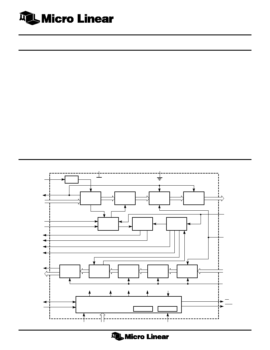
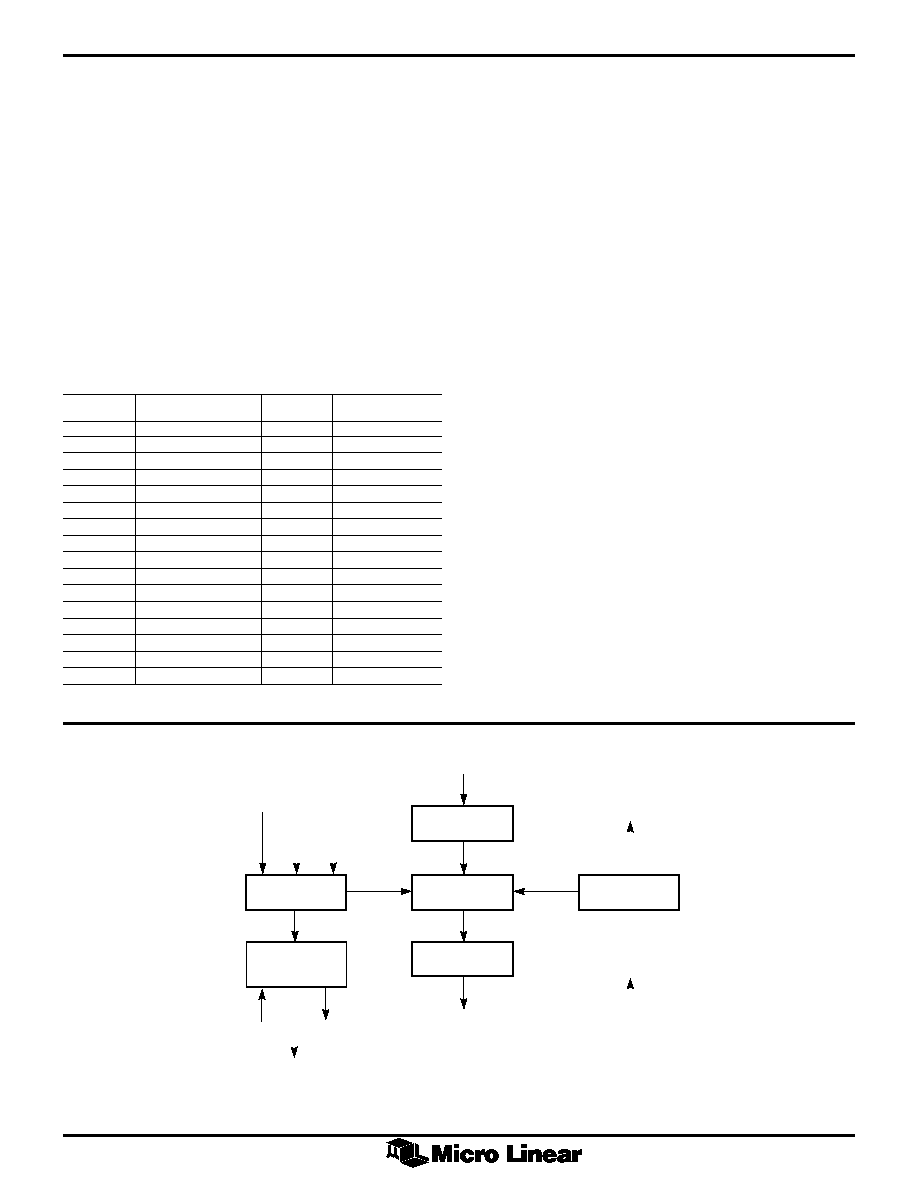
GENERAL DESCRIPTION
The ML6691 implements the upper portion of the physical
layer for the Fast Ethernet 100BASE-T standard. Functions
contained in the ML6691 include a 4B/5B encoder/
decoder, a Stream Cipher scrambler/descrambler, and
collision detect. Additional functions of the ML6691 --
accessible through the two-wire MII management
interface -- include full duplex operation, loopback,
power down mode, and MII isolation.
The ML6691 is designed to interface to a 100BASE-T
Ethernet Media Access Controller (MAC) via the MII
(Media Independent Interface) on one side, and a
100BASE-X PMD transceiver on the other side. A
complete 100BASE-TX physical layer (PHY) solution is
realized using the ML6691, the ML6673, and one of the
available clock recovery/generation devices. A 100BASE-
FX physical layer solution is implemented by disabling the
scrambler function of the ML6691 and using an external
* This Part Is End Of Life As Of August 1, 2000
optical PMD.
BLOCK DIAGRAM
OSC
NIBBLE
INPUT
REGISTER
4B/5B
ENCODER
STREAM
CIPHER
SCRAMBLER
SYMBOL
OUTPUT
REGISTER
TRANSMIT
STATE
MACHINE
COLLISION
DETECTION
RECEIVE
STATE
MACHINE
NIBBLE
OUTPUT
REGISTER
5B/4B
DECODER
SYMBOL
ALIGNER
STREAM
CIPHER
DESCRAMBLER
SYMBOL
INPUT
REGISTER
MANAGEMENT SECTION
CONTROL
STATUS
ISOLATE
FULLDUP
COLTST
LPBK
LINK FAILED
LOCAL
AD4...AD0
RST
MDIO
MDC
RXCLK
RXD3
RXD0
...
RXER
RXDV
CRS
COL
TXER
TXEN
TXCLK
TXD3
TXD0
...
TXC
V
CC
GND
TSM4
TSM0
...
SD
DCFR
RXC
RSM4
RSM0
...
LPBK
CS
ML6691
2
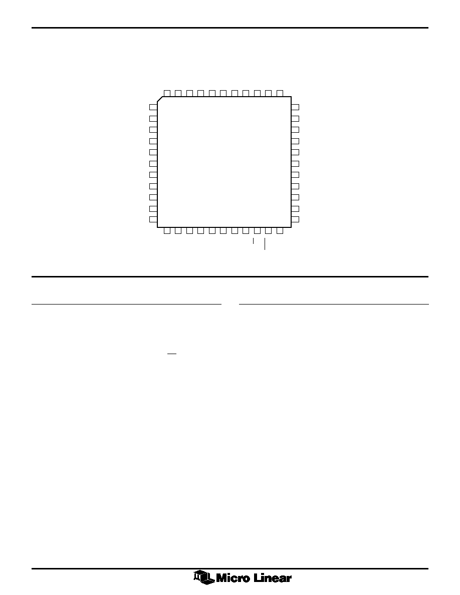
PIN CONFIGURATION
ML6691
44-PIN PLCC (Q44)
TSM4
TSM3
TSM2
TSM1
TSM0
SD
RSM4
RSM3
RSM2
RSM1
RSM0
TXER
TXD3
TXD2
TXD1
TXD0
CRS
COL
RXD3
RXD2
RXD1
RXD0
18
19 20
21
22
TXEN
TXCLK
AD4
AD3
AD2
V
CC
AD1
AD0
MDC
MDIO
TXC
RXDV
RXER
RXCLK
V
CC
DCFR
GND
LOCAL
RST
CS
LPBK
RXC
23
24
7
8
9
10
11
12
13
14
15
16
17
6
5
4
3
2
39
38
37
36
35
34
33
32
31
30
29
1
44
25
43
26
42
27
41
28
40
PIN#
NAME
FUNCTION
1,21
V
CC
Positive 5 volt supply.
2,3,4,
AD[4:0]
Local PHY address. These 5 inputs set
43,44
the address to which the local physical
layer responds. When an address
match is detected, the CS output is
asserted.
5
TXCLK
Transmit clock output. Continuous
25MHz clock provides the timing
reference for the transfer of TXEN,
TXER, and TXD[3:0] from the MAC.
TXCLK is generated from the TXC
input.
6
TXEN
Transmit enable input. A logic high
enables the transmit section of the
ML6691. This signal indicates the
MAC is transmitting nibble-wide data.
TXEN is synchronous to TXCLK.
7
TXER
Transmit error input. When TXER is
high , while TXEN is asserted, the
ML6691 will insert an "H" symbol in
the data stream. TXER is synchronous
to TXCLK.
8-11
TXD[3:0] Transmit nibble data inputs. Nibble-
wide data from the MAC. For data
transmission TXEN must be asserted.
TXD[0] is the least significant bit.
TXD[3:0] is synchronous to TXCLK.
PIN DESCRIPTION
12
CRS
Carrier sense output. A logic high
indicates that either the transmit or
receive medium is non-idle. CRS is
deasserted when both transmit and
receive are idle.
13
COL
Collision detect output. A logic high
indicates a collision (simultaneous
transmit and receive in half duplex
mode).
14-17
RXD[3:0] Receive nibble data outputs. Nibble-
wide data for transmission to the MAC.
RXD[0] is the least significant bit.
RXD[3:0] is synchronous to RXCLK.
18
RXDV
Receive data valid output. A logic high
indicates the ML6691 is presenting
valid nibble-wide data. RXDV shall
remain asserted from the first
recovered nibble of the frame through
the final recovered nibble. RXDV will
be de-asserted prior to the first RXCLK
that follows the final nibble. RXDV is
synchronous to RXCLK.
19
RXER
Receive error output. Active high,
indicates that a coding error was
detected. RXER is synchronous to
RXCLK.
PIN#
NAME
FUNCTION

ML6691
3
PIN DESCRIPTION
(Continued)
PIN#
NAME
FUNCTION
20
RXCLK
Receive clock output. Continuous
25 MHz clock provides the timing
reference for the transfer of RXDV,
RXER, and RXD[3:0] to the MAC.
22
DCFR
Scrambler/descrambler disable. A
logic high on this input disables the
Stream Cipher scrambler/descrambler.
23
GND
Ground
24
LOCAL
Local/remote. A logic low on this input
places the ML6691 in remote mode, in
which the MII interface is disabled at
power on or after a reset operation.
When low, the isolate bit of the
Control register will be set upon power
up or reset.
25
RST
Reset. A logic high on this input resets
the Status and Control registers to their
default states.
26
CS
Chip select. A logic low is generated
on this output when the ML6691
detects an address match.
27
LPBK
Loopback. A logic low on this output
indicates the loopback function.
28
RXC
Receive symbol clock. A 25 MHz
clock input from the PMD layer. The
rising edge of RXC is used to sample
RSM[4:0].
PIN#
NAME
FUNCTION
29-33
RSM[4:0] Receive symbol data inputs. Symbol-
wide (encoded) data from the PMD
layer.
34
SD
Signal detect. A logic high on this
input indicates the presence of non-
quiet data. The internal signal, linkfail,
is enabled 330
µ
s after SD is asserted.
35-39
TSM[4:0] Transmit symbol data outputs. Symbol-
wide (encoded) data for transfer to the
PMD layer.
40
TXC
Transmit symbol clock input. Input
used to generate TXCLK. Use either a
25 MHz crystal or a 25 MHz clock
between TXC input and GND.
41
MDIO
Management data input/output. A
bi-directional signal used to transfer
control and status information
between the ML6691 and the MAC.
MDIO is synchronous to MDC.
42
MDC
Management data clock input. A low-
frequency aperiodic clock used as the
timing reference for transfer of
information on the MDIO signal.
ML6691
4
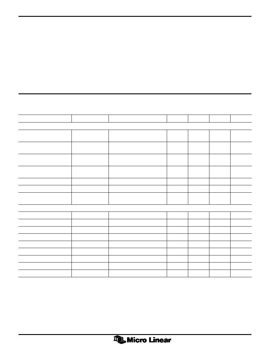
ABSOLUTE MAXIMUM RATINGS
Absolute maximum ratings are those values beyond which
the device could be permanently damaged. Absolute
maximum ratings are stress ratings only and functional
device operation is not implied.
Supply Voltage (V
CC
) ................................................ 6.0V
GND ................................................ ≠0.3V to V
CC
+ 0.3V
Logic Inputs ..................................... ≠0.3V to V
CC
+ 0.3V
Input Current per Pin............................................
±
25mA
Storage Temperature .............................. ≠65
∞
C to +150
∞
C
Package Dissipation at T
A
= 25
∞
C ....................... 750mW
Lead Temperature (soldering 10 sec.) ..................... 300
∞
C
OPERATING CONDITIONS
Supply Voltage (V
CC
) .................................... 4.5V to 5.5V
Temperature Range ................................ 0
∞
C < T
A
< 70
∞
C
ELECTRICAL CHARACTERISTICS
Unless otherwise specified, V
CC
= 5V
±
10%, C
L
= 15pF, T
A
= T
MIN
to T
MAX
PARAMETER
SYMBOL
CONDITIONS
MIN
TYP
MAX
UNITS
DC Characteristics
Logic Input Low
V
IL
All except TXC
0.8
V
TXC
1.5
Logic Input High
V
IH
All except TXC
2.0
V
TXC
3.5
Logic Input Low Current
I
IL
V
IN
= 0, all except TXC
≠10
µ
A
V
IN
= 0, TXC
≠100
Logic Input High Current
I
IH
V
IN
= V
CC
, all except TXC
10
µ
A
V
IN
= V
CC
, TXC
100
Logic Output Low
V
OL
I
OL
= ≠4mA
0.4
V
Logic Output High
V
OH
I
OH
= 4mA
2.4
V
Input Capacitance
C
IN
All except TXC
8
pF
TXC
12
AC Characteristics
TXD Setup Time
t
1
15
ns
TXD Hold Time
t
2
0
ns
TXC to TSM Delay
t
3
5
25
ns
RSM Setup Time
t
4
10
ns
RSM Hold Time
t
5
5
ns
RXCLK to RXD Delay
t
6
0
10
ns
MDIO Setup Time
t
7
10
ns
MDIO Hold time
t
8
10
ns
MDC to MDIO Delay
t
9
0
300
ns
ML6691
5
TXCLK
TXEN, TXER, TXD[3:0]
t1
t2
Transmit Timing Relationships (MII Interface)
Transmit Timing Relationships (Physical Interface)
RXC
RSM[4:0]
t4
t5
Receive Timing Relationships (Physical Interface)
RXCLK
RXDV, RXER, RXD[3:0]
t6
MDC
MDIO
t7
t8
MDC
MDIO
t9
Receive Timing Relationships (MII Interface)
Management Timing Relations (Sourced by STA)
Management Timing Relations (Sourced by PHY)
TXCLK
TXEN
TXER
TXD[3:0]
TSM[4:0]
I
J
K
H
T
R
I
Transmission Timing
RXCLK
RXDV
RXER
RSM[4:0]
RXD[3:0]
0000
I
J
K
H
T
R
I
0101
0000
Receiving Timing
TXC
TSM[4:0]
t3
ML6691
6
FUNCTIONAL DESCRIPTION
To describe the function of the ML6691, the device is
separated into three sections, the Transmit Section, the
Receive Section, and the Management section. Each
section is discussed below.
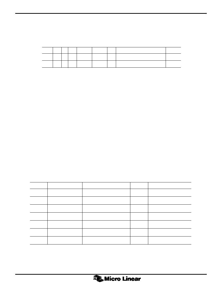
TRANSMIT SECTION
The transmit section is responsible for converting transmit
nibble data on the MII lines from the MAC into encoded
and ciphered transmit symbols, as shown in Figure 1. The
nibble input register samples the transmit nibble data on
the MII lines and passes the nibble data onto the encoder.
The encoder then converts the data to 4B/5B code (see
Table 1) under the direction of the state machine. The
state machine detects the leading edges of transmit enable
and impresses the start of frame delimiter -- the JK pair --
ignoring the TXD<3:0> during these two symbol times. If,
while transmit enable is asserted, the transmit error is
asserted, the H symbol will be impressed except during
the time the JK pair is emitted. Following the trailing edge
of transmit enable, the end of frame delimiter -- the TR
pair -- is generated, after which the IDLE symbol is
generated to fill the space between frames. The encoded
data is then enciphered by performing a XOR with the
output of the cipher register.
The cipher register is a linear feedback shift register which
generates the cipher bit stream which is used to scramble
the transmit symbol data. The Boolean algebra expression
is listed below.
TCFR11 = TCFR6
TCFR10 = TCFR5
TCFR9 = TCFR4
TCFR8 = TCFR3
TCFR7 = TCFR2
TCFR6 = NOT (TCFR11 OR TCFR10 OR TCFR9 OR
TCFR8 OR TCFR7 OR TCFR6 OR TCFR5 OR
TCFR4 OR TCFR3 OR TCFR2) OR TCFR1
TCFR5 = TCFR11 XOR TCFR9
TCFR4 = TCFR10 XOR TCFR8
TCFR3 = TCFR9 XOR TCFR7
TCFR2 = TCFR8 XOR TCFR6
TCFR1 = TCFR7 XOR TCFR5
The enciphered data are then passed to the symbol output
register which drives the generated symbol data out to the
PMD transceiver.
Collision detect is implemented by noting the occurrence
of reception during transmission. A linkfail indication at
any time causes an immediate transition to the IDLE state
and supersedes any other transmit operation.
Figure 1. Transmit Section Block Diagram
HEX/4B
SYMBOL/5B
HEX/4B
SYMBOL/5B
0000
11110
J
11000
0001
01001
K
10001
0010
10100
T
01101
0011
10101
R
00111
0100
01010
H
00100
0101
01011
IDLE
11111
0110
01110
0111
01111
1000
10010
1001
10011
1010
10110
1011
10111
1100
11010
1101
11011
1110
11100
1111
11101
Table 1. 4B/5B Encoding Table
TRANSMIT
ERROR
(TXER)
LINK
FAIL
TRANSMIT
STATE MACHINE
ENCODER/
ENCIPHER
SYMBOL OUTPUT
REGISTER
CARRIER AND
COLLISION
DETECT
NIBBLE INPUT
REGISTER
CIPHER
REGISTER
TRANSMIT NIBBLE
CLOCK
(TXCLK)
TRANSMIT
ENABLE
(TXEN)
TRANSMIT SYMBOL CLOCK
(TXC)
TRANSMIT NIBBLE DATA
(TXD[3:0])
TRANSMIT SYMBOL DATA
(TSM[4:0])
RECEIVING
TRANSMITTING
COLLISION
(COL)
CARRIER SENSE
(CRS)
ML6691
7
RECEIVE SECTION
The receive section is responsible for converting received
unaligned symbols into deciphered, aligned and decoded
nibble data on the MII lines, as shown in Figure 2. The
receive symbol input register samples the receive symbol
data from the PMD transceiver and passes the symbol data
onto the decipher process. The cipher lock is restored by
reloading the decipher register after detecting 13
consecutive IDLE symbols which must occur between
packets. The decipher function is then performed by an
exclusive-OR of the output of the decipher register and
the input symbols.
The decipher symbol data are then passed to the symbol
aligner. The symbols are broken into arbitrary five-bit
groups. The alignment is achieved by scanning the code-
bit stream for the JK pair following the idle symbols.
The decoder translates the 4B/5B coded deciphered and
aligned symbols into hex nibbles. The decoder along with
the state machine also examines the symbol stream for
packet framing information. The JK is converted back to
55 and the TR into 00. The decoder also flags invalid
symbol codes and generates the receive error signal. The
state machine also generates the receive data valid signal.
A premature stream termination is caused by the detection
of two IDLE symbols prior to an TR. A linkfail signal will
also terminate the receive operation immediately.
Note, the "Bad SSD" state is not implemented in the
receive state machine of the ML6691.
Figure 2. Receive Section Block Diagram
LINK
FAIL
RECEIVE
STATE MACHINE
DECIPHER
SYMBOL ALIGNER
SYMBOL INPUT
REGISTER
DECIPHER LOCK
SUBSECTION
RECEIVE SYMBOL
CLOCK
(RXC)
RECEIVING
DECODER
NIBBLE OUTPUT
REGISTER
RECEIVE NIBBLE CLOCK
(RXCLK)
RECEIVE SYMBOL DATA
(RSM[4:0])
RECEIVE NIBBLE DATA
(RXD[3:0])
RECEIVE
ERROR
(RXER)
RECEIVE
DATA VALID
(RXDV)
ML6691
8
MANAGEMENT SECTION
The ML6691 implements the applicable portions of the
IEEE 802.3 Control and Status registers. The management
section provides a two-wire serial interface for the
purpose of control and status gathering. The MDIO pin is
a bi-directional signal used to transfer control information
between the ML6691 and the MAC. Data on MDIO is
clocked using the MDC pin. The following frame structure
is used:
PRE (Preamble)
The preamble condition on the two wire interface is a
logic one. Prior to initiation of any other transaction, a
sequence of 32 consecutive logic ones must be presented
on MDIO with 32 corresponding cycles on MDC to
establish synchronization.
ST (Start of Frame)
The start of frame is indicated by a <01> pattern. This
pattern assures transitions from the default logic one line
state to zero and back to one.
OP (Operation Code)
The operation code for a read transaction is <10>, while
the operation code for a write transaction is <01>.
PHYAD (PHY Address)
The PHY Address is five bits, allowing 32 unique PHY
addresses. The first PHY address bit transmitted and
received is the MSB of the address.
REGAD (Register Address)
The Control register is address <00000>, and the Status
register is address <00001>.
TA (Turnaround)
The turnaround time is a 2 bit time spacing between the
Register Address field and the Data field of a management
frame to avoid contention during a read transaction.
DATA (Data)
The data field is 16-bits. The first data bit transmitted and
received shall be bit 15 of the register being addressed.
CONTROL REGISTER
Table 2 shows the applicable portions of the Control
registers that are implemented in the ML6691. Bits 12, 9,
and 6≠0 are read-only and have default values of logic
low.
PRE ST
OP
PHYAD
REGAD
TA
DATA
IDLE
READ
1
01
10
AAAAA
RRRRR
Z0
DDDDDDDDDDDDDDDD
Z
WRITE
1
01
01
AAAAA
RRRRR
10
DDDDDDDDDDDDDDDD
Z
CONTROL REGISTER
BIT
NAME
DESCRIPTION
R/W
DEFAULT
15
Reset
1 = reset
R/W
0
0 = normal operation
SC
14
Loopback
1 = loopback
R/W
0
0 = normal operation
13
Speed Selection
1 = 100Mb/s
R
1
0 = 10Mb/s
11
Power Down
1 = power down
R/W
0
0 = normal operation
10
Isolate
1= electrically isolate from MII
R/W
Determined by LOCAL
0 = normal operation
8
Duplex Mode
1 = full duplex
R/W
0
0 = half duplex
7
Collision Test
1 = test Col signal
R/W
0
0 = normal operation
NOTE:
R/W = Read/Write, SC = Self Clearing
Table 2. Control Register
ML6691
9
Reset: By setting this bit to a logic one, the Control register
will be reset to its default values. This bit self-clears upon
completion of the reset operation.
Loopback: By setting this bit to a logic one, the LPBK pin
will be held at a logic low. The COL signal will remain
low at all times, unless bit 7 is set, in which case the COL
signal shall behave as described.
Speed Selection: This bit is read-only and set at a logic
one by default.
Power Down: By setting this bit to a logic one, the
oscillator and all the MII input buffers except for MDIO
and MDC will be shut down.
Isolate: By setting this bit a logic one, the ML6691 can be
electrically isolated from the MII. In the isolation mode,
the input TXEN will be ignored and TXD[3:0] and TXER
shall not have any effect on the transmit section. All the
output buffers connected to the MII will be tri-stated. The
default state of this bit is determined by the LOCAL pin.
Duplex Mode: ML6691 will operate in Full Duplex mode
when this bit is set to a logic one. The COL signal will
remain low unless bit 7 is set.
Collision Test: By setting this bit to a logic one, the COL
signal will be asserted in response to the assertion of
TXEN, and will continue to assert the COL signal until
TXEN is deasserted.
STATUS REGISTER
Table 3 shows the applicable portions of the Status register
that are implemented in the ML6691. Bits 15, 12-3, 1, and
0 are read-only and have default values of logic low.
100BASE-TX Full Duplex
ML6691 can perform full duplex link transmission and
reception using the 100BASE-TX signaling specification.
This bit is always read as a logic one.
100BASE-TX Half Duplex
ML6691 can perform half duplex link transmission and
reception using the 100BASE-TX signaling specification.
This bit is always read as a logic one.
Link Status
When read as a logic one, this bit indicates that a valid
link has been established. The link status bit is
implemented with a latching function, such that the
occurrence of a link failure condition will cause the link
status bit to become cleared and remain cleared until it is
read via the management interface.
STATUS REGISTER
BIT
NAME
DESCRIPTION
R/W
14
100Base-TX
1 = able to perform full duplex
R/O
Full Duplex
0 = not able to perform full duplex
13
100Base-TX
1 = able to perform full duplex
R/O
Half Duplex
0 = not able to perform full duplex
2
Link Status
1 = link is up
R/O
0 = link is down
LL
NOTE:
R/O = Read Only,
LL = Latching Low
Table 3. Status Register
ML6691
1
0
ORDERING INFORMATION
Micro Linear reserves the right to make changes to any product herein to improve reliability, function or design.
Micro Linear does not assume any liability arising out of the application or use of any product described herein,
neither does it convey any license under its patent right nor the rights of others. The circuits contained in this
data sheet are offered as possible applications only. Micro Linear makes no warranties or representations as to
whether the illustrated circuits infringe any intellectual property rights of others, and will accept no responsibility
or liability for use of any application herein. The customer is urged to consult with appropriate legal counsel
before deciding on a particular application.
DS6691-01
2092 Concourse Drive
San Jose, CA 95131
Tel: 408/433-5200
Fax: 408/432-0295
PART NUMBER
TEMPERATURE RANGE
PACKAGE
ML6691CQ
0
∞
C to 70
∞
C
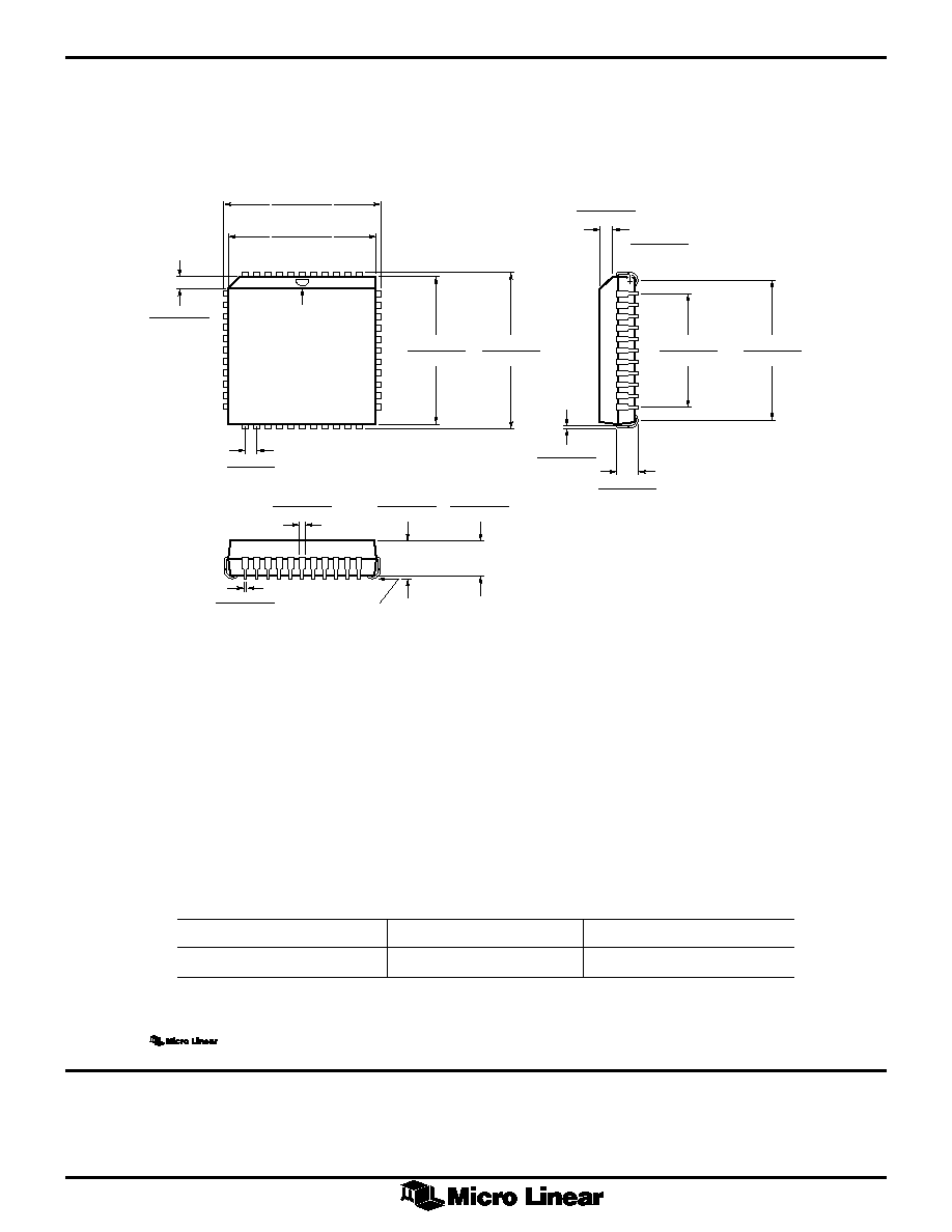
44-PIN PLCC (Q44)
(End Of Life)
0.100 - 0.112
(2.54 - 2.84)
PIN 1 ID
SEATING PLANE
0.685 - 0.695
(17.40 - 17.65)
0.650 - 0.656
(16.51 - 16.66)
0.013 - 0.021
(0.33 - 0.53)
0.165 - 0.180
(4.06 - 4.57)
1
0.650 - 0.656
(16.51 - 16.66)
0.685 - 0.695
(17.40 - 17.65)
12
23
34
0.590 - 0.630
(14.99 - 16.00)
0.025 - 0.045
(0.63 - 1.14)
(RADIUS)
0.050 BSC
(1.27 BSC)
0.009 - 0.011
(0.23 - 0.28)
0.042 - 0.056
(1.07 - 1.42)
0.042 - 0.048
(1.07 - 1.22)
0.026 - 0.032
(0.66 - 0.81)
0.500 BSC
(12.70 BSC)
Package: Q44
44-Pin PLCC
0.148 - 0.156
(3.76 - 3.96)
PHYSICAL DIMENSIONS
inches (millimeters)
© Micro Linear 1997
is a registered trademark of Micro Linear Corporation
Products described in this document may be covered by one or more of the following patents, U.S.: 4,897,611; 4,964,026; 5,027,116; 5,281,862; 5,283,483; 5,418,502; 5,508,570; 5,510,727; 5,523,940;
5,546,017; 5,559,470; 5,565,761; 5,592,128; 5,594,376; Japan: 2598946. Other patents are pending.