December 1998
PRELIMINARY
ML6695
100BASE-X Fiber Physical Layer With 5-bit Interface
1
GENERAL DESCRIPTION
The ML6695 implements the physical layer of the Fast
Ethernet 100BASE-X standard for fiber media. The device
provides the 5-bit (or symbol) interface for interface to
upper-layer silicon. The ML6695 integrates the data
quantizer and the LED driver, allowing the use of low cost
optical PMD components.
The ML6695 includes 125MHz clock recovery/clock
generation, an LED driver, and a data quantizer (post
amplifier). The device also offers a power down mode
which results in total power consumption of less than 20mA.
The ML6695 is suitable for the current 100BASE-FX IEEE
803.2u standard defined using 1300nm optics, as well as
for the
proposed 100BASE-SX standard defined using lower
cost 820nm optics.
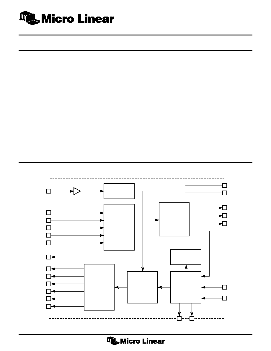
BLOCK DIAGRAM
FEATURES
s
100BASE-FX physical layer with 5-bit interface
s
Optimal 100BASE-SX solution (draft standard)
s
Integrated data quantizer (post-amplifier)
s
Integrated LED driver
s
125MHz clock generation and recovery
s
Power-down mode
TXC
TSM4
TSM3
TSM2
TSM1
TSM0
RXC
RSM4
RSM3
RSM2
RSM1
RSM0
VIN�
VIN+
PWRDN
LPBK
SDO
SERIALIZER
NRZ TO NRZI
ENCODER
DESERIALIZER
CLOCK & DATA
RECOVERY
NRZI TO NRZ
DECODER
CLOCK
SYNTHESIZER
SIGNAL
DETECT
IOUT
IOUT
RTSET
CAPDC
CAPB
DATA QUANTIZER
(POST AMPLIFIER)
LED
DRIVER
2
ML6695
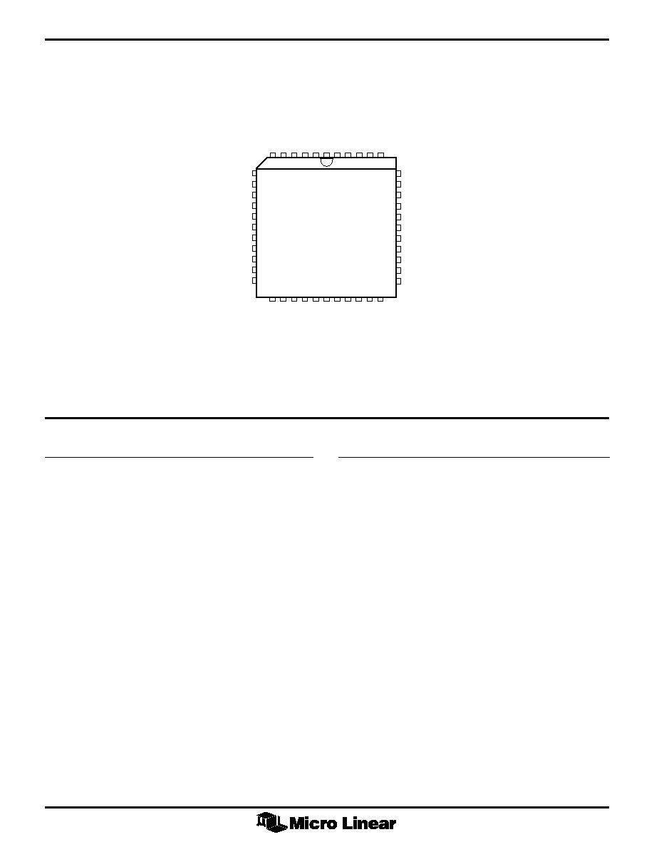
PIN CONFIGURATION
PIN DESCRIPTION
TOP VIEW
ML6695
44-Pin PLCC (Q44)
PWRDN
RSM4
RSM3
DGND1
RSM2
DVCC1
RSM1
DGND2
RSM0
RXC
DGND3
IOUT
IOUT
AGND3
RTSET
AVCC3A
AVCC3B
AVCC4A
AGND4A
AVCC4B
VIN+
VIN�
TSM0
TSM1
TSM2
TSM3
TSM4
AGND1
TXC
AV
CC
1
LPBK
AV
CC
2
AGND2
SDO
DVCC2
DGND4C
DGND4B
DGND4A
DV
CC
5
DGND5B
DGND5A
CAPDC
CAPB
AGND4B
7
8
9
10
11
12
13
14
15
16
17
39
38
37
36
35
34
33
32
31
30
29
18 19 20 21 22 23 24 25 26 27 28
6 5 4 3 2 1 44 43 42 41 40
PIN
NAME
FUNCTION
1
A
GND
1
Analog ground
2
TSM4
Transmit data TTL inputs. TSM 0-4
inputs accept TX data symbols
from the MII. Data appearing at
TSM 0-4 are clocked into the
ML6695 on the rising edge of
TXCLK .
3
TSM3
Transmit data TTL inputs. TSM 0-4
inputs accept TX data symbols
from the MII. Data appearing at
TSM 0-4 are clocked into the
ML6695 on the rising edge of
TXC.
4
TSM2
Transmit data TTL inputs. TSM 0-4
inputs accept TX data symbols
from the MII. Data appearing at
TSM 0-4 are clocked into the
ML6695 on the rising edge of
TXC.
PIN
NAME
FUNCTION
5
TSM1
Transmit data TTL inputs. TSM 0-4
inputs accept TX data symbols
from the MII. Data appearing at
TSM 0-4 are clocked into the
ML6695 on the rising edge of TXC.
6
TSM0
Transmit data TTL inputs. TSM 0-4
inputs accept TX data symbols
from the MII. Data appearing at
TSM 0-4 are clocked into the
ML6695 on the rising edge of TXC.
7
PWRDN
Powerdown TTL input. Driving this
pin low, or floating the pin, powers
the ML6695 down to a low-
current, inoperative state. Driving
PWRDN high enables the
ML6695.
8
RSM4
Receive data TTL outputs. RSM 0-
4 output may be sampled
synchronously with RXC's rising
edge.

ML6695
3
PIN
NAME
FUNCTION
9
RSM3
Receive data TTL outputs. RSM 0-
4 output may be sampled
synchronously with RXC's rising
edge.
10
DGND1
Digital ground
11
RSM2
Receive data TTL outputs. RSM 0-
4 output may be sampled
synchronously with RXC's rising
edge.
12
DV
CC
1
Digital positive power supply
13
RSM1
Receive data TTL outputs. RSM 0-
4 output may be sampled
synchronously with RXC's rising
edge.
14
DGND2
Digital ground
15
RSM0
Receive data TTL outputs. RSM 0-
4 output may be sampled
synchronously with RXC's rising
edge.
16
RXC
Recovered receive symbol clock
TTL output. This 25MHz clock is
phase-aligned with the internal
125MHz bit clock recovered from
the signal received at V
IN+/�
.
Receive data are clocked out at
RSM 0-4 on the falling edges of
this clock.
17
DGND3
Digital ground
18
SDO
Signal Detect TTL output. This
output goes high when the signal
at VIN+/- exceeds the preset
amplitude threshold.
19
DV
CC
2
Digital positive power supply
20
DGND4C
Digital ground
21
DGND4B
Digital ground
22
DGND4
Digital ground
23
DV
CC
5
Digital positive power supply
24
DGND5B
Digital ground
25
DGND5A
Digital ground
PIN
NAME
FUNCTION
26
CAPDC
Data quantizer offset-correction
loop, offset-storage capacitor input
pin. The capacitor tied between
this pin and AV
CC
stores the
amplified data quantizer offset
voltage and also sets the dominant
pole in the offset-correction loop.
A 0.1�F surface mount is
recommended.
27
CAPB
Data quantizer input bias bypass
capacitor input. The capacitor tied
between this pin and AV
CC
filters
the quantizer's internal input bias
reference. A 0.1�F surface-mount
capacitor is recommended.
28
AGND4B
Analog ground
29
V
IN
�
Receive quantizer input. This
differential input pair receives
100BASE-FX NRZI signals from the
network opto-coupler.
30
V
IN
+
Receive quantizer input. This
differential input pair receives
100BASE-FX NRZI signals from the
network opto-coupler.
31
AV
CC
4B
Analog positive power supply
32
AGND4A
Analog ground
33
AV
CC
4A
Analog positive power supply
34
AV
CC
3B
Analog positive power supply
35
AV
CC
3A
Analog positive power supply
36
RTSET
Transmit level bias resistor. For
100BASE-FX, an external 2.32k
W,
1% resistor connected between
RTSET and AGND3 sets a
precision constant bias current
that gives a nominal output "on"
current of 75mA at I
OUT
.
37
AGND3
Analog ground
38
IOUT
Transmit LED output. This pin
connects through an external 15
W
resistor to AV
CC
when the part is
used to drive a network LED.
PIN DESCRIPTION
(Continued)

4
ML6695
PIN DESCRIPTION
(Continued)
PIN
NAME
FUNCTION
39
IOUT
Transmit LED output. This open-
collector current output drives
NRZI waveforms into an LED.
Output current can be set
externally by choosing RTSET
value.
40
AGND2
Analog ground
41
AV
CC
2
Analog positive power supply
42
LPBK
Loopback TTL input pin. Tying this
pin to ground places the part in
loopback mode; data at TSM0 0-4
are serialized, then sent to the
quantizer, followed by the receive
PLL for clock recovery, and finally
to the RSM<4:07> outputs.
Floating this pin or tying it to V
CC
places the part in its normal mode
of operation.
PIN
NAME
FUNCTION
43
AV
CC
1
Analog positive power supply
44
TXC
Transmit clock TTL input. This
25MHz clock is phase-aligned
with the internal 125MHz TX bit
clock. Data appearing at
Tsm<4:0> are clocked into the
ML6695 on the rising edge of this
clock.
ML6695
5
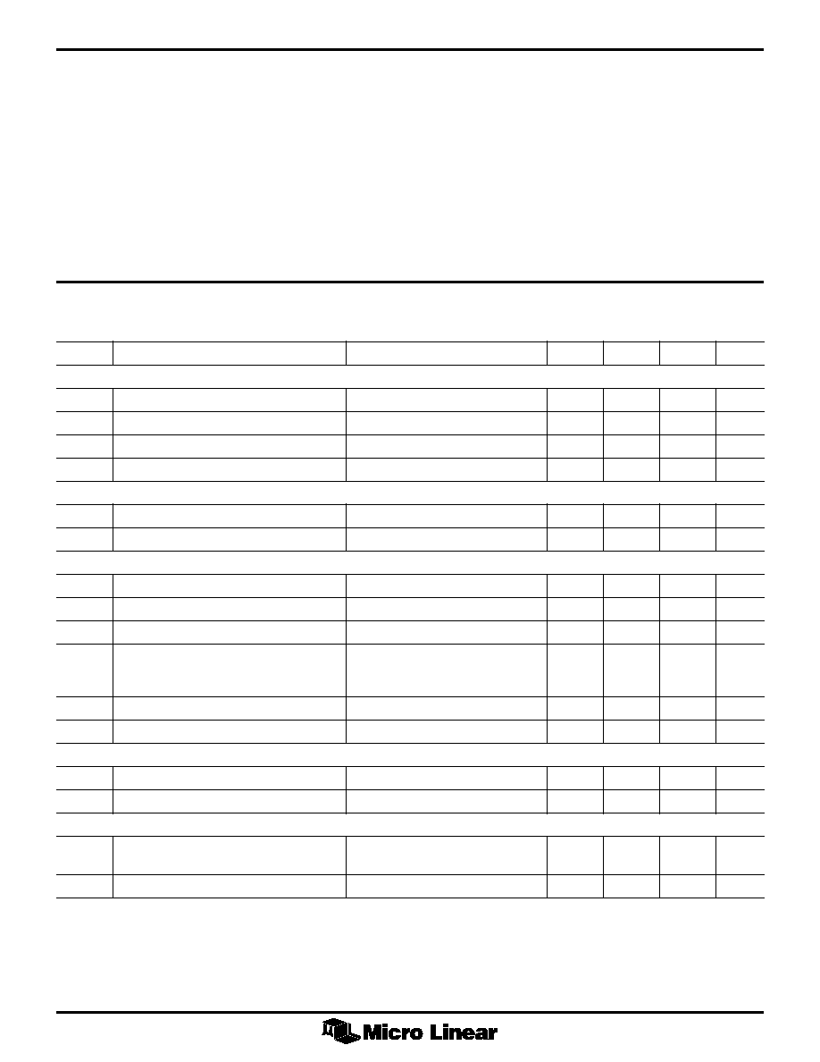
ABSOLUTE MAXIMUM RATINGS
Absolute maximum ratings are those values beyond which
the device could be permanently damaged. Absolute
maximum ratings are stress ratings only and functional
device operation is not implied.
V
CC
Supply Voltage Range ............................ �0.3V to 6V
Input Voltage Range
Digital Inputs ........................................... �0.3V to V
CC
VIN+, VIN-,TXC, CAPDC, CAPB ............... �0.3V to V
CC
Output Current
IOUT, IOUT ........................................................ 90mA
All Other Outputs ............................................... 10mA
Junction Temperature .................................... 0�C to 125�C
Storage Temperature ................................. �65�C to 150�C
Lead Temperature (Soldering, 10 sec) ..................... 260�C
Thermal Resistance (
q
JA
)
PLCC ............................................................... 53�C/W
OPERATING CONDITIONS
Temperature Range ....................................... 0�C to 70�C
V
CC
Supply Voltage .............................. ........... 5V �5%
All V
CC
supply pins
must be within 0.1V of each other.
All GND pins
must be within 0.1V of each other.
DC ELECTRICAL CHARACTERISTICS
Unless otherwise specified, V
CC
= 5V �5%, T
A
= Operating Temperature Range (Note 1)
SYMBOL
PARAMETER
CONDITIONS
MIN
TYP
MAX
UNITS
TTL INPUTS (TSM<4:0>, LPBK, TXC, PWRDN)
V
IL
Input Low Voltage
I
IL
= �400�A
�0.3
0.8
V
V
IH
Input High Voltage
I
IH
= 100�A
2.0
V
CC
+0.3
V
I
IL
Input Low Current
V
IN
= 0.4V
�200
�A
I
IH
Input High Current
V
IN
= 2.4V
100
�A
TTL OUTPUTS (RSM<4:0>, RXC, SDO)
V
OL
Output Low Voltage
I
OL
= 4mA
0.4
V
V
OH
Output High Voltage
I
OH
= �4mA
2.4
RECEIVER
V
ICM
V
IN
+/- input common-mode voltage
V
CC
= 5V
2.5
V
V
ID
V
IN
+/- differential input voltage range
3.5
1700
mV
P-P
R
IDR
V
IN
+/- differential input resistance
500
1k
W
V
SDA
Signal detect assertion threshold
peak-to-peak non-idle
8
12
mV
P-P
signal level at V
IN
+/- for
SDO assertion
A
HYST
Input hysteresis
1.5
2
dB
I
RT
RTSET input current
RTSET = 2.32k
W �1%
486
540
594
�A
TRANSMITTER
I
LEDH
I
OUT
high output current (Note 2)
RTSET = 2.32k
W �1%
67.5
75
82.5
mA
I
LEDL
I
OUT
/I
OUT
low output current
RTSET = 2.32k
W �1%
0.1
mA
POWER SUPPLY CURRENT
I
CC
Supply Current, 100BASE-FX operation,
Current into all V
CC
pins,
200
295
mA
transmitting
V
CC
= 5.25V
I
PD
Supply Current, Powerdown Mode
20
mA
6
ML6695
AC ELECTRICAL CHARACTERISTICS
Unless otherwise specified, V
CC
= 5V �5%, T
A
= Operating Temperature Range (Note 1)
SYMBOL
PARAMETER
CONDITIONS
MIN
TYP
MAX
UNITS
TRANSMITTER (NOTE 8)
t
TR/F
I
OUT
rise/fall time
Note 3
2
ns
t
TDC
I
OUT
output duty cycle distortion
Note 3
-0.5
0.5
ns
SIGNAL DETECT
t
AS
SDO assert time (SDO low to high)
VIN>8mV
P-P
100
�s
t
ANS
SDO deassert time (SDO high to low)
VIN<8mV
P-P
350
�s
DATA INTERFACE
X
NTOL
TX input clock frequency tolerance
25MHz frequency
�50
50
ppm
t
TPWH
TXC pulse width HIGH
14
ns
t
TPWL
TXC pulse width LOW
14
ns
t
RPWH
RXC pulse width HIGH
14
ns
t
RPWL
RXC pulse width LOW
14
ns
t
TPS
Setup time, TSM 0-4 data valid to
13
ns
TXC rising edge (1.4V point)
t
TPH
Hold time, TSM 0-4 data valid after
3
ns
TXC rising edge (1.4V point)
t
RCS
Time that RSM0-4 data are valid
10
ns
before RXC falling edge (1.4V point)
t
RCH
Time that RSM0-4 data are valid
10
ns
after RXC falling edge (1.4V point)
t
RPCR
RXC 10%-90% rise time
6
ns
t
RPCF
RXC 90%-10% fall time
6
ns
Note 1. Limits are guaranteed by 100% testing, sampling, or correlation with worst case test conditions.
Note 2. Output current amplitude is I
OUT
= 207V/RTSET.
Note 3. Using the test load shown in Figure 1, transmitting "H" symbols.

ML6695
7
FUNCTIONAL DESCRIPTION
TRANSMIT SECTION
The ML6695 transmit section accepts parallel NRZ data
nibbles, creates a serial NRZI data stream using the
internal 125MHz clock multiplier, and provides an open-
collector output IOUT to directly drive an LED. IOUT
must be connected to V
CC
through a 15
W resistor. The
internal clock multiplier accepts an external 25MHz
clock input.
The LED driver at IOUT is a current mode switch which
develops the output light by sinking current through the
network LED into IOUT. RTSET'S value determines the
output current:
RTSET
V
IOUT
=
�
125
140
.
W
(1)
where IOUT is the desired output current.
RECEIVE SECTION
The ML6695 receive section includes a fiber optic
quantizer and a 125MHz receive clock recovery circuit.
The quantizer is a wide-bandwidth limiting amplifier with
DC offset correction. The quantizer output drives a data
comparator with a controlled slicing threshold. The
comparator provides a large-amplitude receive signal. The
clock recovery circuit extracts 125MHz receive clock
from the large-amplitude signal, and provides the clock
for the parallel data output registers. Received NRZ data
nibbles appear at the RSM outputs synchronously with
RXC falling edges. Received signals exceeding the preset
signal detect amplitude threshold for more than 5�s cause
the SDO output to go high. Received signals that fall
below the preset threshold for more than 5�s cause SDO
to go low.
OTHER MODES
The ML6695 will enter a power down mode when the
PWRDN pin is tied low. In this state the ML6695 powers
down to a low-current (less than 20mA), inoperative state.
Driving it high enables normal operation of the ML6695.
Loopback mode is entered when the LPBK is tied to
ground. In this mode, the data at TSM0-4 are serialized,
then sent to the quantizer, followed by the receive PLL for
clock recovery, and finally to the RSM0-4 outputs. Tying
LPBK to V
CC
places the ML6695 in its normal mode of
operation.
IOUT
IOUT
38
39
ML6695
15
15
Figure 1. Test Load
8
ML6695
DS6695-01
ORDERING INFORMATION
PART NUMBER
TEMPERATURE RANGE
PACKAGE
ML6695CQ
0�C to 70�C
44-Pin PLCC (Q44)
� Micro Linear 2000.
is a registered trademark of Micro Linear Corporation. All other trademarks are the
property of their respective owners.
Products described herein may be covered by one or more of the following U.S. patents: 4,897,611; 4,964,026; 5,027,116;
5,281,862; 5,283,483; 5,418,502; 5,508,570; 5,510,727; 5,523,940; 5,546,017; 5,559,470; 5,565,761; 5,592,128; 5,594,376;
5,652,479; 5,661,427; 5,663,874; 5,672,959; 5,689,167; 5,714,897; 5,717,798; 5,742,151; 5,747,977; 5,754,012; 5,757,174;
5,767,653; 5,777,514; 5,793,168; 5,798,635; 5,804,950; 5,808,455; 5,811,999; 5,818,207; 5,818,669; 5,825,165; 5,825,223;
5,838,723; 5.844,378; 5,844,941. Japan: 2,598,946; 2,619,299; 2,704,176; 2,821,714. Other patents are pending.
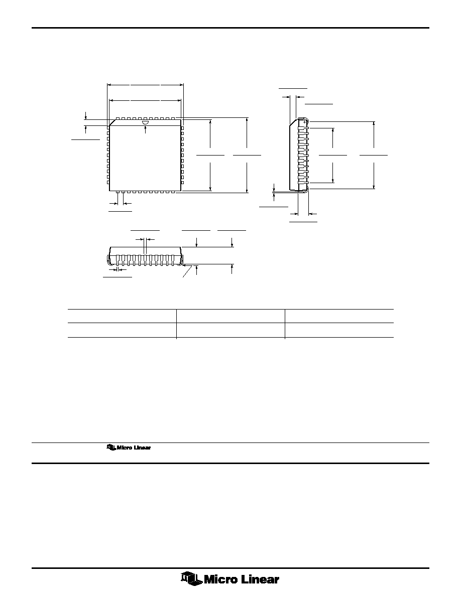
PHYSICAL DIMENSIONS
inches (millimeters)
0.100 - 0.112
(2.54 - 2.84)
PIN 1 ID
SEATING PLANE
0.685 - 0.695
(17.40 - 17.65)
0.650 - 0.656
(16.51 - 16.66)
0.013 - 0.021
(0.33 - 0.53)
0.165 - 0.180
(4.06 - 4.57)
1
0.650 - 0.656
(16.51 - 16.66)
0.685 - 0.695
(17.40 - 17.65)
12
23
34
0.590 - 0.630
(14.99 - 16.00)
0.025 - 0.045
(0.63 - 1.14)
(RADIUS)
0.050 BSC
(1.27 BSC)
0.009 - 0.011
(0.23 - 0.28)
0.042 - 0.056
(1.07 - 1.42)
0.042 - 0.048
(1.07 - 1.22)
0.026 - 0.032
(0.66 - 0.81)
0.500 BSC
(12.70 BSC)
Package: Q44
44-Pin PLCC
0.148 - 0.156
(3.76 - 3.96)
2092 Concourse Drive
San Jose, CA 95131
Tel: (408) 433-5200
Fax: (408) 432-0295
www.microlinear.com
Micro Linear makes no representations or warranties with respect to the accuracy, utility, or completeness of the contents
of this publication and reserves the right to make changes to specifications and product descriptions at any time without
notice. No license, express or implied, by estoppel or otherwise, to any patents or other intellectual property rights is granted
by this document. The circuits contained in this document are offered as possible applications only. Particular uses or
applications may invalidate some of the specifications and/or product descriptions contained herein. The customer is urged
to perform its own engineering review before deciding on a particular application. Micro Linear assumes no liability
whatsoever, and disclaims any express or implied warranty, relating to sale and/or use of Micro Linear products including
liability or warranties relating to merchantability, fitness for a particular purpose, or infringement of any intellectual property
right. Micro Linear products are not designed for use in medical, life saving, or life sustaining applications.