 | –≠–ª–µ–∫—Ç—Ä–æ–Ω–Ω—ã–π –∫–æ–º–ø–æ–Ω–µ–Ω—Ç: 12C672 | –°–∫–∞—á–∞—Ç—å:  PDF PDF  ZIP ZIP |

©
1998 Microchip Technology Inc.
DS40175A-page 1
PIC12C67X AND PIC12CE67X
This document includes the programming
specifications for the following devices:
1.0
PROGRAMMING THE
PIC12C67X AND PIC12CE67X
The PIC12C67X and PIC12CE67X can be pro-
grammed using a serial method. In serial mode the
PIC12C67X and PIC12CE67X can be programmed
while in the users system. This allows for increased
design flexibility.
1.1
Hardware Requirements
The PIC12C67X and PIC12CE67X requires two pro-
grammable power supplies, one for V
DD
(2.0V to 6.0V
recommended) and one for V
PP
(12V to 14V). Both
supplies should have a minimum resolution of 0.25V.
1.2
Programming Mode
The programming mode for the PIC12C67X and
PIC12CE67X allows programming of user program
memory, special locations used for ID, and the configu-
ration word for the PIC12C67X and PIC12CE67X.
∑ PIC12C671
∑ PIC12C672
∑ PIC12CE673
∑ PIC12CE674
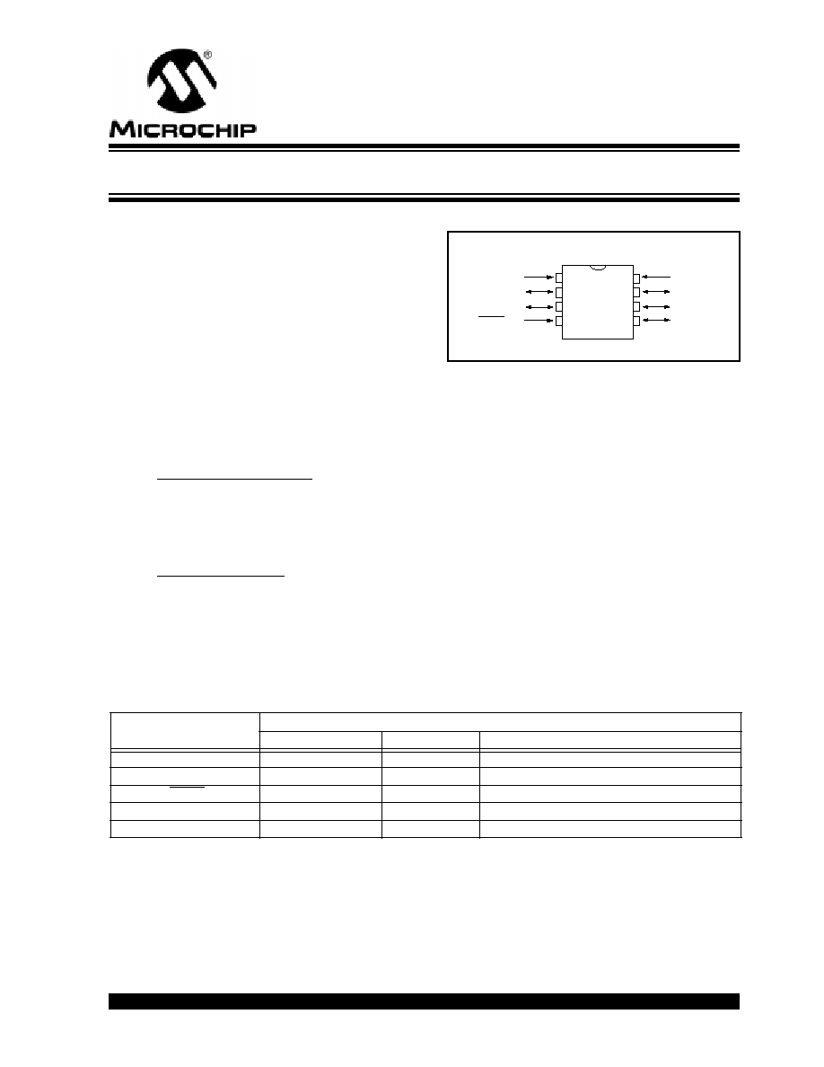
Pin Diagram:
PDIP
8
7
6
5
1
2
3
4
PIC12C67X
GP5/OSC1/CLKIN
GP4/OSC2/AN3/
GP3/MCLR/V
PP
V
DD
V
SS
GP0/AN0
GP1/AN1/V
REF
GP2/T0CKI/
AN2/INT
CLKOUT
PIC12CE67X
EPROM Memory Programming Specification
PIN DESCRIPTIONS (DURING PROGRAMMING): PIC12C671/672 and PIC12CE673/674
Pin Name
During Programming
Pin Name
Pin Type
Pin Description
GP1
CLOCK
I
Clock input
GP0
DATA
I/O
Data input/output
GP3/MCLR/V
PP
V
PP
P
Programming Power
V
DD
V
DD
P
Power Supply
V
SS
V
SS
P
Ground
Legend: I = Input, O = Output, P = Power

PIC12C67X and PIC12CE67X
DS40175A-page 2
©
1998 Microchip Technology Inc.
2.0
PROGRAM MODE ENTRY
2.1
User Program Memory Map
The user memory space extends from 0x0000 to
0x1FFF (8K). Table 2-1 shows actual implementation
of program memory in the PIC12C67X family.
TABLE 2-1:
IMPLEMENTATION OF
PROGRAM MEMORY IN THE
PIC12C67X
When the PC reaches the last location of the imple-
mented program memory, it will wrap around and
address a location within the physically implemented
memory (see Figure 2-1).
In programming mode the program memory space
extends from 0x0000 to 0x3FFF, with the first half
(0x0000-0x1FFF) being user program memory and the
second half (0x2000-0x3FFF) being configuration
memory. The PC will increment from 0x0000 to
0x1FFF and wrap to 0x000 or 0x2000 to 0x3FFF and
wrap around to 0x2000 (not to 0x0000). Once in con-
figuration memory, the highest bit of the PC stays a '1',
thus always pointing to the configuration memory. The
only way to point to user program memory is to reset
the part and reenter program/verify mode, as described
in Section 2.2.
The last location of the program memory space holds
the factory programmed oscillator calibration value.
This location should not be programmed except when
blank (a non-blank value should not cause the device
to fail a blank check). If blank, the programmer should
program it to a RETLW XX statement where "XX" is the
calibration value.
Device
Program Memory Size
PIC12C671/
PIC12CE673
0x000 - 0x3FF (1K)
PIC12C672/
PIC12CE674
0x000 - 0x7FF (2K)
In the configuration memory space, 0x2000-0x20FF
are utilized. When in configuration memory, as in the
user memory, the 0x2000-0x2XFF segment is repeat-
edly accessed as the PC exceeds 0x2XFF (see
Figure 2-1).
A user may store identification information (ID) in four
ID locations. The ID locations are mapped in [0x2000 :
0x2003].
Note 1:
All other locations in PIC configuration
memory are reserved and should not be
programmed.
Note 2:
Due to the secure nature of the on-board
EEPROM memory in the
PIC12CE673/674, it can be accessed only
by the user program.

©
1998 Microchip Technology Inc.
DS40175A-page 3
EPROM Memory Programming Specification
FIGURE 2-1:
PROGRAM MEMORY MAPPING
0
3FF
400
7FF
800
BFF
C00
FFF
1000
1FFF
2000
2008
2100
3FFF
ID Location
ID Location
ID Location
ID Location
Reserved
Reserved
Reserved
Configuration Word
2000
2001
2002
2003
2004
2005
2006
2007
1FF
1KW
2KW
Implemented
Implemented
Implemented
Reserved
Reserved
Reserved
Reserved
Reserved
Reserved

PIC12C67X and PIC12CE67X
DS40175A-page 4
©
1998 Microchip Technology Inc.
2.2
Program/Verify Mode
The program/verify mode is entered by holding pins
GP1 and GP0 low while raising MCLR pin from V
IL
to
V
IHH
(high voltage). VDD is then raised from VIL to
VIH.Once in this mode the user program memory and
the configuration memory can be accessed and pro-
grammed in serial fashion. The mode of operation is
serial, and the memory that is accessed is the user pro-
gram memory. GP1 is a Schmitt Trigger input in this
mode.
The sequence that enters the device into the program-
ming/verify mode places all other logic into the reset
state (the MCLR pin was initially at V
IL
). This means
that all I/O are in the reset state (High impedance
inputs).
1.0.1
PROGRAM/VERIFY OPERATION
The GP1 pin is used as a clock input pin, and the GP0
pin is used for entering command bits and data
input/output during serial operation. To input a com-
mand, the clock pin (GP1) is cycled six times. Each
command bit is latched on the falling edge of the clock
with the least significant bit (LSB) of the command
being input first. The data on pin GP0 is required to
Note 1:
The MCLR pin must be raised from V
IL
to
V
IHH
before V
DD
is applied. This is to
ensure that the device does not have the
PC incremented while in valid operation
range.
Note 2:
Do not power GP2, GP4 or GP5 before
V
DD
is applied.
have a minimum setup and hold time (see AC/DC
specs) with respect to the falling edge of the clock.
Commands that have data associated with them (read
and load) are specified to have a minimum delay of 1
µ
s
between the command and the data. After this delay
the clock pin is cycled 16 times with the first cycle being
a start bit and the last cycle being a stop bit. Data is
also input and output LSB first. Therefore, during a
read operation the LSB will be transmitted onto pin
GP0 on the rising edge of the second cycle, and during
a load operation the LSB will be latched on the falling
edge of the second cycle. A minimum 1
µ
s delay is also
specified between consecutive commands.
All commands are transmitted LSB first. Data words
are also transmitted LSB first. The data is transmitted
on the rising edge and latched on the falling edge of the
clock. To allow for decoding of commands and reversal
of data pin configuration, a time separation of at least
1
µ
s is required between a command and a data word
(or another command).
The commands that are available are listed
in
Table
1-1.
1.0.1.1
LOAD CONFIGURATION
After receiving this command, the program counter
(PC) will be set to 0x2000. By then applying 16 cycles
to the clock pin, the chip will load 14-bits a "data word"
as described above, to be programmed into the config-
uration memory. A description of the memory mapping
schemes for normal operation and configuration mode
operation is shown in Figure 2-1. After the configuration memory is entered, the only way to get back to the user pro-
gram memory is to exit the program/verify test mode by taking MCLR low (V
IL
).
TABLE 1-1:
COMMAND MAPPING
Command
Mapping (MSB ... LSB)
Data
Load Configuration
0
0
0
0
0
0
0, data(14), 0
Load Data
0
0
0
0
1
0
0, data(14), 0
Read Data
0
0
0
1
0
0
0, data(14), 0
Increment Address
0
0
0
1
1
0
Begin programming
0
0
1
0
0
0
End Programming
0
0
1
1
1
0

©
1998 Microchip Technology Inc.
DS40175A-page 5
EPROM Memory Programming Specification
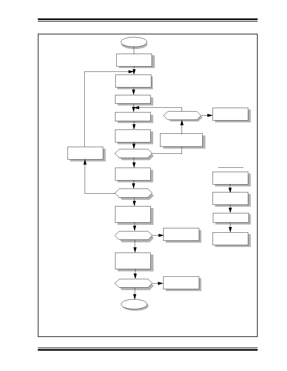
FIGURE 1-1:
PROGRAM FLOW CHART - PIC12C67X AND PIC12CE67X PROGRAM MEMORY
Start
Set V
DD
= V
DDP
∑
N = N + 1
Load Data
Command
Increment Address
Command
Report Verify
@ V
DD
MAX
Error
End Programming
Command
Begin Programming
Command
Apply 3N Additional
Program Cycles
Read Data
Command
Program Cycle
Program Cycle
N > 25
Data Correct?
Done
No
Yes
Yes
No
No
Yes
Set V
PP
= V
IHH1
N = 0
All Locations Done?
Verify all Locations
@ V
DD
MIN
.∑
V
PP
= V
IHH2
Data Correct?
Yes
Verify all Locations
@ V
DD
MAX
.
V
PP
= V
IHH2
Data Correct?
Yes
Report Programming
Failure
Wait 100
µ
s
Report Verify
@ V
DD
MIN
.
Error
No
No
∑
V
DDP
=
V
DD
range for programming (typically 4.75V - 5.25V).
V
DD
MIN
.
= Minimum
V
DD
for device operation.
V
DD
MAX
.
= Maximum
V
DD
for device operation.
N = # of Program Cycles


