 | –≠–ª–µ–∫—Ç—Ä–æ–Ω–Ω—ã–π –∫–æ–º–ø–æ–Ω–µ–Ω—Ç: 24AA64 | –°–∫–∞—á–∞—Ç—å:  PDF PDF  ZIP ZIP |
©
1998 Microchip Technology Inc.
DS21189B-page 1
M
DEVICE SELECTION TABLE
FEATURES
∑ Low power CMOS technology
- Maximum write current 3 mA at 5.5V
- Maximum read current 400
µ
A at 5.5V
- Standby current 100 nA typical at 5.5V
∑ 2-wire serial interface bus, I
2
C compatible
∑ Cascadable for up to eight devices
∑ Self-timed ERASE/WRITE cycle
∑ 32-byte page or byte write modes available
∑ 5 ms max write cycle time
∑ Hardware write protect for entire array
∑ Output slope control to eliminate ground bounce
∑ Schmitt trigger inputs for noise suppression
∑ 1,000,000 erase/write cycles guaranteed
∑ Electrostatic discharge protection > 4000V
∑ Data retention > 200 years
∑ 8-pin PDIP, SOIC (150 and 208 mil) and TSSOP
packages; 14-pin SOIC package
∑ Temperature ranges:
DESCRIPTION
The Microchip Technology Inc. 24AA64/24LC64
(24xx64*) is a 8K x 8 (64K bit) Serial Electrically Eras-
able PROM capable of operation across a broad volt-
age range (1.8V to 5.5V). It has been developed for
advanced, low power applications such as personal
communications or data acquisition. This device also
has a page-write capability of up to 32 bytes of data.
This device is capable of both random and sequential
reads up to the 64K boundary. Functional address lines
allow up to eight devices on the same bus, for up to 512
Kbits address space. This device is available in the
standard 8-pin plastic DIP, 8-pin SOIC (150 and
208 mil), and 8-pin TSSOP.
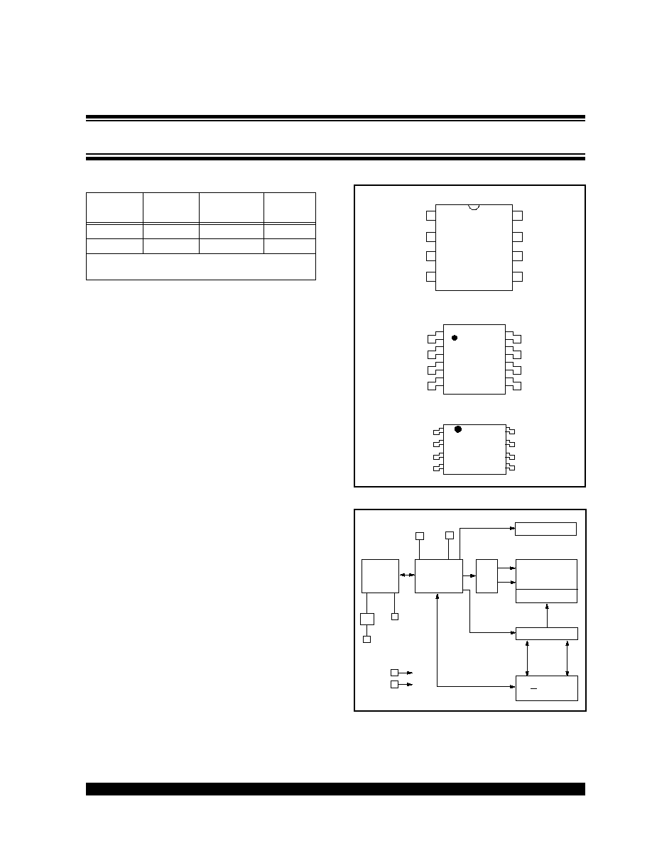
PACKAGE TYPE
BLOCK DIAGRAM
Part
Number
Vcc
Range
Max Clock
Frequency
Temp
Ranges
24AA64
1.8-5.5V
400 kHz
I
24LC64
2.5-5.5V
400 kHz
I, E
100 kHz for Vcc < 2.5V.
100 kHz for E temperature range.
- Industrial (I):
-40
∞
C to
+85
∞
C
- Automotive (E)
-40
∞
C to +125
∞
C
A0
A1
A2
Vss
Vcc
WP
SCL
SDA
1
2
3
4
8
7
6
5
1
2
3
4
8
7
6
5
24xx64
24xx64
PDIP
TSSOP
WP
Vcc
A0
A1
SCL
SDA
Vss
A2
A0
A1
A2
V
SS
V
CC
WP
SCL
SDA
24xx64
1
2
3
4
8
7
6
5
SOIC
HV GENERATOR
EEPROM
ARRAY
PAGE LATCHES
YDEC
XDEC
SENSE AMP
R/W CONTROL
MEMORY
CONTROL
LOGIC
I/O
CONTROL
LOGIC
A0...A2
SDA
SCL
V
CC
V
SS
WP
I/O
I
2
C is a trademark of Philips Corporation.
*24xx64 is used in this document as a generic part number for the 24AA64/24LC64 devices.
24AA64/24LC64
64K I
2
C
TM
CMOS Serial EEPROM
24AA64/24LC64
DS21189B-page 2
©
1998 Microchip Technology Inc.
1.0
ELECTRICAL
CHARACTERISTICS
1.1
Maximum Ratings*
Vcc .................................................................................................7.0V
All inputs and outputs w.r.t. Vss............................... -0.6V to Vcc +1.0V
Storage temperature ................................................... -65∞C to +150∞C
Ambient temp. with power applied............................... -65∞C to +125∞C
Soldering temperature of leads (10 seconds) ........................... +300∞C
ESD protection on all pins...........................................................
4 kV
*Notice: Stresses above those listed under "Maximum Ratings" may
cause permanent damage to the device. This is a stress rating only and
functional operation of the device at those or any other conditions
above those indicated in the operational listings of this specification is
not implied. Exposure to maximum rating conditions for extended peri-
ods may affect device reliability.
TABLE 1-1
PIN FUNCTION TABLE
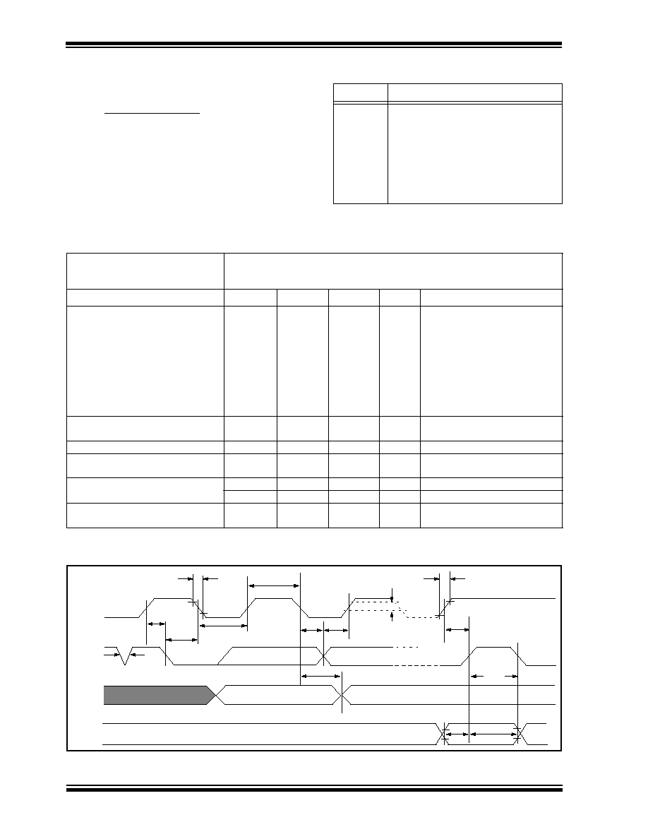
FIGURE 1-1:
BUS TIMING DATA
Name
Function
A0,A1,A2
User Configurable Chip Selects
V
SS
Ground
SDA
Serial Data
SCL
Serial Clock
WP
Write Protect Input
V
CC
+1.8 to 5.5V (24AA64)
+2.5 to 5.5V (24LC64)
TABLE 1-2
DC CHARACTERISTICS
All parameters apply across the
recommended operating ranges
unless otherwise noted.
Industrial (I):
V
CC
= +1.8V to 5.5V
Tamb = -40
∞
C to +85
∞
C
Automotive (E): V
CC
= 4.5V to 5.5V
Tamb = -40
∞
C to 125
∞
C
Parameter
Symbol
Min
Max
Units
Conditions
A0, A1, A2,
SCL, SDA, and WP pins:
High level input voltage
V
IH
0.7 V
CC
--
V
Low level input voltage
V
IL
--
0.3 V
CC
0.2 V
CC
V
V
V
CC
2.5V
V
CC
< 2.5V
Hysteresis of Schmitt Trigger
inputs (SDA, SCL pins)
V
HYS
0.05 V
CC
--
V
V
CC
> 2.5V (Note)
Low level output voltage
V
OL
--
0.40
V
I
OL
= 3.0 mA @ V
CC
= 4.5V
I
OL
= 2.1 mA @ V
CC
= 2.5V
Input leakage current
I
LI
-10
10
µ
A
V
IN
= Vss to V
CC
, WP = V
SS
V
IN
= Vss or V
CC
, WP = V
CC
Output leakage current
I
LO
-10
10
µ
A
V
OUT
= Vss to V
CC
Pin capacitance
(all inputs/outputs)
C
IN
, C
OUT
--
10
pF
V
CC
= 5.0V (Note)
Tamb = 25∞C, f
c
= 1 MHz
Operating current
I
CC
Write
--
3
mA
V
CC
= 5.5V
I
CC
Read
--
400
µ
A
V
CC
= 5.5V, SCL = 400 kHz
Standby current
I
CCS
--
1
µ
A SCL = SDA = V
CC
= 5.5V
A0, A1, A2, WP = V
SS
Note:
This parameter is periodically sampled and not 100% tested.
WP
(unprotected)
(protected)
T
SU
:
WP
T
HD
:
WP
SCL
SDA
IN
T
SU
:
STA
SDA
OUT
T
HD
:
STA
T
LOW
T
HIGH
T
R
T
BUF
T
AA
T
HD
:
DAT
T
SU
:
DAT
T
SU
:
STO
T
SP
T
F
V
HYS

©
1998 Microchip Technology Inc.
DS21189B-page 3
24AA64/24LC64
TABLE 1-3
AC CHARACTERISTICS
All parameters apply across the spec-
ified operating ranges unless other-
wise noted.
Industrial (I):
V
CC
= +1.8V to 5.5V
Tamb = -40
∞
C to +85
∞
C
Automotive (E): V
CC
= +4.5V to 5.5V
Tamb = -40
∞
C to 125
∞
C
Parameter
Symbol
Min
Max
Units
Conditions
Clock frequency
F
CLK
--
--
--
100
100
400
kHz
4.5V
V
CC
5.5V (E Temp range)
1.8V
V
CC
2.5V
2.5V
V
CC
5.5V
Clock high time
T
HIGH
4000
4000
600
--
--
--
ns
4.5V
V
CC
5.5V (E Temp range)
1.8V
V
CC
2.5V
2.5V
V
CC
5.5V
Clock low time
T
LOW
4700
4700
1300
--
--
--
ns
4.5V
V
CC
5.5V (E Temp range)
1.8V
V
CC
2.5V
2.5V
V
CC
5.5V
SDA and SCL rise time
(Note 1)
T
R
--
--
--
1000
1000
300
ns
4.5V
V
CC
5.5V (E Temp range)
1.8V
V
CC
2.5V
2.5V
V
CC
5.5V
SDA and SCL fall time
T
F
--
300
ns
(Note 1)
START condition hold time
T
HD
:
STA
4000
4000
600
--
--
--
ns
4.5V
V
CC
5.5V (E Temp range)
1.8V
V
CC
2.5V
2.5V
V
CC
5.5V
START condition setup time
T
SU
:
STA
4700
4700
600
--
--
--
ns
4.5V
V
CC
5.5V (E Temp range)
1.8V
V
CC
2.5V
2.5V
V
CC
5.5V
Data input hold time
T
HD
:
DAT
0
--
ns
(Note 2)
Data input setup time
T
SU
:
DAT
250
250
100
--
--
--
ns
4.5V
V
CC
5.5V (E Temp range)
1.8V
V
CC
2.5V
2.5V
V
CC
5.5V
STOP condition setup time
T
SU
:
STO
4000
4000
600
--
--
--
ns
4.5V
V
CC
5.5V (E Temp range)
1.8V
V
CC
2.5V
2.5V
V
CC
5.5V
WP setup time
T
SU
:
WP
4000
4000
600
--
--
--
ns
4.5V
V
CC
5.5V (E Temp range)
1.8V
V
CC
2.5V
2.5V
V
CC
5.5V
WP hold time
T
HD
:
WP
4700
4000
1300
--
--
--
ns
4.5V
V
CC
5.5V (E Temp range)
1.8V
V
CC
2.5V
2.5V
V
CC
5.5V
Output valid from clock
(Note 2)
T
AA
--
--
--
3500
3500
900
ns
4.5V
V
CC
5.5V (E Temp range)
1.8V
V
CC
2.5V
2.5V
V
CC
5.5V
Bus free time: Time the bus must be
free before a new transmission can
start
T
BUF
4700
4700
1300
--
--
--
ns
4.5V
V
CC
5.5V (E Temp range)
1.8V
V
CC
2.5V
2.5V
V
CC
5.5V
Output fall time from V
IH
minimum to V
IL
maximum
T
OF
10
250
ns
C
B
100 pF (Note 1)
Input filter spike suppression
(SDA and SCL pins)
T
SP
--
50
ns
(Notes 1 and 3)
Write cycle time (byte or page)
T
WC
--
5
ms
Endurance
1M
--
cycles
25
∞
C, V
CC
= 5.0V, Block Mode (Note 4)
Note 1:
Not 100% tested. C
B
= total capacitance of one bus line in pF.
2:
As a transmitter, the device must provide an internal minimum delay time to bridge the undefined region (minimum
300 ns) of the falling edge of SCL to avoid unintended generation of START or STOP conditions.
3:
The combined T
SP
and V
HYS
specifications are due to new Schmitt trigger inputs which provide improved noise spike
suppression. This eliminates the need for a TI specification for standard operation.
4:
This parameter is not tested but guaranteed by characterization. For endurance estimates in a specific application, please
consult the Total Endurance Model which can be obtained on Microchip's BBS or website.
24AA64/24LC64
DS21189B-page 4
©
1998 Microchip Technology Inc.
2.0
PIN DESCRIPTIONS
2.1
A0, A1, A2 Chip Address Inputs
The A0,A1,A2 inputs are used by the 24xx64 for multi-
ple device operation. The levels on these inputs are
compared with the corresponding bits in the slave
address. The chip is selected if the compare is true.
Up to eight devices may be connected to the same bus
by using different chip select bit combinations. These
inputs must be connected to either V
CC
or V
SS
.
2.2
SDA Serial Data
This is a bi-directional pin used to transfer addresses
and data into and data out of the device. It is an open-
drain terminal, therefore, the SDA bus requires a pullup
resistor to V
CC
(typical 10 k
for 100 kHz, 2 k
for
400 kHz)
For normal data transfer SDA is allowed to change only
during SCL low. Changes during SCL high are
reserved for indicating the START and STOP condi-
tions.
2.3
SCL Serial Clock
This input is used to synchronize the data transfer from
and to the device.
2.4
WP
This pin can be connected to either Vss, Vcc or left
floating. An internal pull-down resistor on this pin will
keep the device in the unprotected state if left floating.
If tied to Vss or left floating, normal memory operation
is enabled (read/write the entire memory 0000-1FFF).
If tied to V
CC
, WRITE operations are inhibited. Read
operations are not affected.
3.0
FUNCTIONAL DESCRIPTION
The 24xx64 supports a bi-directional two-wire bus and
data transmission protocol. A device that sends data
onto the bus is defined as a transmitter, and a device
receiving data as a receiver. The bus must be con-
trolled by a master device which generates the serial
clock (SCL), controls the bus access, and generates
the START and STOP conditions while the 24xx64
works as a slave. Both master and slave can operate as
a transmitter or receiver but the master device deter-
mines which mode is activated.
4.0
BUS CHARACTERISTICS
The following bus protocol has been defined:
∑ Data transfer may be initiated only when the bus
is not busy.
∑ During data transfer, the data line must remain
stable whenever the clock line is HIGH. Changes
in the data line while the clock line is HIGH will be
interpreted as a START or STOP condition.
Accordingly, the following bus conditions have been
defined (Figure 4-1).
4.1
Bus not Busy (A)
Both data and clock lines remain HIGH.
4.2
Start Data Transfer (B)
A HIGH to LOW transition of the SDA line while the
clock (SCL) is HIGH determines a START condition.
All commands must be preceded by a START condi-
tion.
4.3
Stop Data Transfer (C)
A LOW to HIGH transition of the SDA line while the
clock (SCL) is HIGH determines a STOP condition. All
operations must end with a STOP condition.
4.4
Data Valid (D)
The state of the data line represents valid data when,
after a START condition, the data line is stable for the
duration of the HIGH period of the clock signal.
The data on the line must be changed during the LOW
period of the clock signal. There is one clock pulse per
bit of data.
Each data transfer is initiated with a START condition
and terminated with a STOP condition. The number of
the data bytes transferred between the START and
STOP conditions is determined by the master device.
4.5
Acknowledge
Each receiving device, when addressed, is obliged to
generate an acknowledge signal after the reception of
each byte. The master device must generate an extra
clock pulse which is associated with this acknowledge
bit.
A device that acknowledges must pull down the SDA
line during the acknowledge clock pulse in such a way
that the SDA line is stable LOW during the HIGH period
of the acknowledge related clock pulse. Of course,
setup and hold times must be taken into account. Dur-
ing reads, a master must signal an end of data to the
slave by NOT generating an acknowledge bit on the
last byte that has been clocked out of the slave. In this
case, the slave (24xx64) will leave the data line HIGH
to enable the master to generate the STOP condition.
Note:
The 24xx64 does not generate any
acknowledge bits if an internal program-
ming cycle is in progress.
©
1998 Microchip Technology Inc.
DS21189B-page 5
24AA64/24LC64
FIGURE 4-1:
DATA TRANSFER SEQUENCE ON THE SERIAL BUS
FIGURE 4-2:
ACKNOWLEDGE TIMING
ADDRESS OR
ACKNOWLEDGE
VALID
DATA
ALLOWED
TO CHANGE
STOP
CONDITION
START
CONDITION
SCL
SDA
(A)
(B)
(D)
(D)
(C)
(A)
SCL
9
8
7
6
5
4
3
2
1
1
2
3
Transmitter must release the SDA line at this point
allowing the Receiver to pull the SDA line low to
acknowledge the previous eight bits of data.
Receiver must release the SDA line at this point
so the Transmitter can continue sending data.
Data from transmitter
Data from transmitter
SDA
Acknowledge
Bit